Thermal-tolerant polymers with antireflective and hydrophobic grooved subwavelength grating surfaces for high-performance optics

Jung Woo Leem, Bhaskar Dudem and Jae Su Yu*
Department of Electronics and Radio Engineering, Kyung Hee University, 1732 Deogyeong-daero, Giheung-gu, Yongin-si, Gyeonggi-do 17104, South Korea. E-mail: jsyu@khu.ac.kr

Received 14th June 2016 , Accepted 17th August 2016

First published on 18th August 2016


Abstract

We report thermal-tolerant polymer films integrated with antireflective and hydrophobic grooved subwavelength gratings (G-SWGs), which are fabricated by a soft imprint lithography from silicon molds with conical SWGs, for high-performance optics. For the poly-dimethylsiloxane (PDMS) polymer films with the G-SWGs at one- and both-side surfaces, their optical properties are investigated for different periods, exhibiting efficient broadband and wide-angle antireflection behavior with light scattering. To simply demonstrate their feasibility in optical and optoelectronic systems, the one-side G-SWGs PDMS film with a short period of 380 nm is laminated on indium tin oxide-coated glass (i.e., ITO glass) and polyethylene terephthalate (PET) substrates. This film effectively enhances the transmittance (or suppresses the reflectance) of both the bare ITO glass and PET substrates in wide ranges of wavelengths and incident angles. Additionally, it shows not only a relatively strong thermal durability at temperatures less than 180 °C, but also a hydrophobic surface with high water contact angle of around 140° (i.e., self-cleaning ability).

Introduction

Light management, including antireflection, light scattering, light trapping, etc., is one of the attractive strategies to improve the optical performance in various optical components and optoelectronic devices such as eye-wear glasses, optical lenses, solar cells, light-emitting diodes, and optical sensors.1–3 To suppress the Fresnel surface reflection losses, as an alternative to conventional thin films with a quarter-wavelength thickness, many studies have been reported on bio-inspired architectures such as subwavelength structures,4,5 nanowires/nanorods,6,7 nanodomes,3 and nanoporous films.8,9 On the other hand, nanotextures or microtextures,10–12 metal particles,13,14 and metal grids15 have been utilized for light scattering (e.g., increase of optical path lengths in a transparent medium or diffraction of light reflected from the rear metal layer) and light trapping (e.g., plasmonic near-field excitation in the interface between dielectric and metal materials). However, for the realization of these nanostructures and microstructures, expansive and complex fabrication methods such as nanolithography patterning (i.e., electron-beam lithography, nanoimprint lithography, photolithography, etc.) and subsequent etching processes including post thermal or chemical treatments are usually required.4,5,10–12 Also, it is difficult to obtain uniformity and reproducibility on the large-area surface. Therefore, it is necessary to develop versatile optical structures in an effective way including facile, cost-effective, and mass-productive manufacturing processes. In this respect, a soft imprint lithography (SIL) method can be one of desirable patterning techniques because of its relative simplicity, low cost, scale tunability, and high-throughput production (e.g., roll-to-roll/roll-to-plate processes).16–18 Furthermore, once the master molds are fabricated, they can be repeatedly employed in pattern transfer processes. In the SIL, conformable and elastomeric poly-dimethylsiloxane (PDMS), which is already commercially available, has been generally utilized for flexible and rigid engineering applications due to its low surface energy, flexibility, transparency, and hardness.17–19 Also, for transparent substrates including glasses, sapphires, plastics, etc. (i.e., n ≥ 1.5), the PDMS, which has the easy lamination (strongly attached) and detachability on a planar surface, as a protective cover-layer enables to enhance their optical behaviors (e.g., antireflection and diffuse light scattering) owing to its lower refractive index (i.e., n ≈ 1.4–1.43) as well as the easy formation of the nanopatterns or micropatterns on its surface.20–22 Besides, for thermal-related applications such as outdoor solar systems, thermal sensors, and other relatively high temperature-exposed optical components (e.g., windows, mirrors, lenses, and filters), a thermal durability of polymer films should be considered. For outdoor environment applications, additionally, the self-cleaning ability, which can remove the pollutants (i.e., dust particles) on the top surface of outdoor systems, is crucial since the optical performance can be degraded due to the interruption of light propagation caused by the surface contaminants.23,24

To the best of our knowledge, however, there is very little report on the optical performance for the polymer films with a nanoscale groove surface at one- and both-sides for different periods, together with a study of their theoretical optical analyses, thermal durability, and surface wettability, including their applications on the flexible and rigid transparent substrates. In this work, we fabricated the grooved subwavelength gratings (G-SWGs) on one- or both-side surfaces of PDMS films using the SIL technique via silicon (Si) molds with conical SWGs for different periods. Their optical properties were experimentally and theoretically investigated at different incident angles of light. For optical analyses, the numerical modeling and simulations were performed by the rigorous coupled-wave analysis (RCWA) and finite difference time-domain (FDTD) methods. The thermal durability and surface wetting behaviors were also explored. To simply show the practical applicability on the transparent substrates, the PDMS films with G-SWGs were laminated on the indium tin oxide (ITO)-coated glass and polyethylene terephthalate (PET) substrates.

Experimental and simulation details

Fabrication of G-SWGs on PDMS films

Fig. 1(a) shows the schematic illustration for the fabrication process of the G-SWGs on the surface of PDMS films using conical SWG-patterned Si molds via a SIL method. To prepare the master mold, the conical grating nanopatterns with two-dimensional (2D) periodic hexagonal arrays were formed on the surface of Si substrates by using laser interference lithography and dry etching processes. Further details can be found in our previous work.25 In order to transfer subwavelength-scale patterns without deformation and distortion on the surface of PDMS films, a hard PDMS (h-PDMS) solution mixed with four components (VDT-731, SIP 6831.1, SIT7900, and HMS-301, Gelest Inc.) was spin-coated on the Si molds, and then the samples were cured in an oven. Subsequently, a soft PDMS (s-PDMS, base resin[thin space (1/6-em)]:[thin space (1/6-em)]curing agent = 10[thin space (1/6-em)]:[thin space (1/6-em)]1) solution, which can suppress pressure and enable conformal contact with the substrate, was poured on the h-PDMS/Si molds, followed by curing. Finally, the PDMS (h-PDMS/s-PDMS) films with G-SWGs patterns at one-side surface (i.e., one-side G-SWGs PDMS, a thickness of ∼200 μm) were obtained by peeling off them from the Si molds. For the both-side G-SWGs PDMS films, two Si molds were used in the SIL process. To investigate the effect of the period of G-SWGs PDMS films on their optical properties, the Si master molds with three periods of 380, 500, and 650 nm used in our previous work were employed.22 Additionally, the surface modification of the G-SWGs PDMS film was performed to further enhance its surface hydrophobicity by dipping the sample into the mixture of 5 μL of trichloro(1H,1H,2H,2H-perfluorooctyl)silane (FOTS) and 5 mL of hexane solution for 30 s and dried in oven at 30 °C for 12 h.
image file: c6ra15499a-f1.tif
Fig. 1 Schematic illustrations for (a) the fabrication process of the G-SWGs on the surface of PDMS films using conical SWG-patterned Si molds via a SIL method and (b) the 3D scale-modified simulation model of the G-SWGs on the PDMS film.

Characterization instruments

Field-emission scanning electron microscope (FE-SEM; LEO SUPRA 55, Carl Zeiss) was used to investigate surface morphologies and patterned profiles of the fabricated samples. The optical characteristics were measured by using a UV-vis-NIR spectrophotometer with an integrating sphere (Cary 5000, Varian). For incident angle-dependent transmittance measurements, a spectroscopic ellipsometry (V-VASE, J. A. Woollam Co. Inc.) was utilized at incident light angles of 10–70° for non-polarized light. The water contact angles were evaluated and averaged at three different positions on the surface of samples by using a contact angle measurement system (Phoenix-300, SEO Co., Ltd) with ∼5 μL droplets of de-ionized water at room temperature.

Numerical modeling and simulations

Fig. 1(b) shows the schematic illustration of the 3D scale-modified simulation model of the G-SWGs on the surface of PDMS film. To design the model, the geometry of the G-SWGs was simply represented in the Cartesian coordinate system by a scalar-valued function of three variables, f(x,y,z). The shape of the G-SWGs, i.e., the empty space (air), can be defined by the following equations:26
 
image file: c6ra15499a-t1.tif(1)
where r is the radius of the circle in xy plane, and DG-SWGs, RG-SWGs, and OT are the depth, the top radius, and the order of taper of G-SWGs, respectively. For the G-SWGs, we assumed that the ratio of the top diameter (i.e., z = 0) of G-SWGs to their period (Rtdp) was set to be 0.8 and the OT value was kept at 1.4, respectively. The thickness of the PDMS film was 200 μm. The refractive index of the PDMS was 1.43. For the RCWA and the FDTD optical calculations, a commercial software (DiffractMOD and FullWave, Rsoft Design) was utilized, respectively. In RCWA simulations, the calculated transmittance values at each wavelength were averaged to remove rapid fluctuations caused by the interference of light reflected at the top and bottom surfaces of the PDMS film. For the light propagation calculations in the FDTD, the Ey, i.e., amplitude of y-polarized electric field, was calculated for the incident plane wave with a slab mode beam profile which was normalized.

Results and discussion

Surface morphologies and patterned profiles

Fig. 2 shows the top-view SEM images of the G-SWGs on PDMS films for different periods (P) of (a) 380 nm, (b) 500 nm, and (c) 650 nm and (d) 40° tilted-view low-magnification SEM image of G-SWGs on the PDMS film with a period of 650 nm (i.e., P650). As can be seen in Fig. 2, the grooved nanoscale grating arrays with a closely-packed 2D periodic hexagonal pattern (i.e., G-SWGs) on the surface of PDMS films were well transferred from the conical SWG-patterned Si molds without any large distinct deformation and distortion by the SIL. From the SEM images, the average depths of G-SWGs were evaluated to be approximately 270, 310, and 350 nm for three periods of 380, 500, and 650 nm, respectively. For all the samples, the Rtdp value was about 0.8. In the SEM image of Fig. 2(d), it can be observed that the G-SWGs (P650) were uniformly well formed on the surface of the PDMS film over a large area, similar to our previous result.22
image file: c6ra15499a-f2.tif
Fig. 2 Top-view SEM images of the G-SWGs on PDMS films for different periods (P) of (a) 380 nm, (b) 500 nm, and (c) 650 nm. (d) 40° tilted-view low-magnification SEM image of G-SWGs on the PDMS film with a period of 650 nm (i.e., P650).

Optical properties

In order to estimate optical behaviors of the PDMS films integrated with G-SWGs at one- and both-side surfaces for different periods, their transmittance properties were experimentally and theoretically investigated in the wavelength range of 350–1100 nm at normal incidence. The measured total (solid lines) and diffuse (dotted lines) transmittance spectra of the G-SWGs PDMS films for three periods of 380, 500, and 650 nm at one- and both-side surfaces are shown in Fig. 3(a) and (b), respectively. As shown in Fig. 3(a), the total transmittance of G-SWGs PDMS films strongly depends on the period of the G-SWGs. The transmittance region lower than 93%, which is a transmittance wavelength band of the flat PDMS film, was shifted towards the longer wavelengths and became broader with increasing the period of the G-SWGs due to the diffraction losses in reflections.22,27–29 If the normal incident light enters the periodic grating structure with a period of P, the angle of the reflected diffraction waves, θr,m, in the m-th diffraction order is given by a well-known grating equation:30 sin[thin space (1/6-em)]θr,m = /Pn, where n is the refractive index of incident medium and λ is the incident wavelength of light. From the equation, the zeroth order diffractive wave is only allowed to propagate in the structure and the others are evanesced when the period of gratings becomes much less than the wavelength of the incident light. Furthermore, the nanogratings with a tapered architecture have the continuously and linearly effective gradient-refractive-index distribution between air and the bulk surface, so called “moth eye effect”.31 Thus, for the G-SWGs PDMS films with much smaller periods than wavelengths of the incident light, the high transmittance region of >93% can be obtained at a broader wavelength band. The one-side G-SWGs (P380) PDMS film showed the higher transmittance spectrum compared to the other samples over a wavelength range of 420–1100 nm, yielding an larger average transmittance (TAT) value of ∼96.2% than that (i.e., TAT ≈ 93.5%) of the flat PDMS film as well as those (i.e., TAT ≈ 93.7 and 93%) of the G-SWGs PDMS films at P500 and P650 in the wavelength region of 400–1100 nm. On the other hand, for the diffuse transmittance, the G-SWGs PDMS films with larger periods exhibited higher values at shorter wavelengths whereas there were almost no diffuse lights in the flat PDMS film. This is attributed to the higher orders of diffraction waves penetrating through the G-SWGs with much larger periods than wavelengths of the incident light, as mentioned above. To characterize the light-scattering property, the haze ratio (H), which is defined by the ratio of the diffuse transmittance (TD) to the total transmittance (TT), i.e., H (%) = TD/TT × 100, is generally used. For the G-SWGs (P650) PDMS film, the average H (HA) value was estimated to be ∼12% at wavelengths of 400–1100 nm (i.e., HA ≈ 6% for the flat PDMS film and HA ≈ 6.9 and 8.3% for the G-SWGs at P380 and P500, respectively). This light scattering can be confirmed from the FDTD simulations. The contour plots of calculated electric field (i.e., Ey) intensity distributions for the incident light propagating from air to the PDMS films with the flat and the G-SWGs (P650) surfaces at λ = 405 and 532 nm (right) and the 2D scale-modified simulation model of G-SWGs used in these calculations (left) are shown in the inset of Fig. 3(a). The simulation results revealed that the G-SWGs (P650) PDMS film generates strong light interferences with an angular spread at λ = 405 and 532 nm, respectively, while there exist no scattered lights for the flat PDMS film at λ = 405 nm. Clearly, the PDMS films with the G-SWGs on the both-side surfaces showed better optical performance in both the total and diffuse transmittance characteristics (i.e., antireflection and light-scattering effects). In Fig. 3(b), the both-side G-SWGs PDMS films had the TAT values of ∼97.6, 94.7, and 92.9% for P380, P500, and P650, respectively. For the G-SWGs (P380) PDMS film, the improvement in the transmission (i.e., antireflection) can be observed from the photograph in the upper inset of Fig. 3(b). For the flat PDMS film, the characters under it are nearly not seen owing to the strongly reflected white fluorescent light at both-side surfaces. For the PDMS film with one-side G-SWGs, similarly, it is also relatively difficult to see the characters due to the light reflection at the rear flat-side surface. However, the PDMS film with both-side G-SWGs exhibits much better readability for the characters below it though there exists a weak white reflected fluorescent light. On the other hand, for the light-scattering properties, the both-side G-SWGs (P650) PDMS film showed the larger diffuse transmittance spectrum, indicating the HA ≈ 15.6%, which is also a higher value than those of the other samples (i.e., HA ≈ 7.1 and 9.7% for the both-side G-SWGs PDMS films at P380 and P500, respectively). This light-diffuse phenomenon is also confirmed from the photograph in the lower inset of Fig. 3(b). The photograph showed the diffracted light patterns obtained from the light penetration through the sample with the both-side G-SWGs (P650) for λ = 405, 532, and 650 nm, respectively. These diffracted light patterns around a center light point indicate the high diffraction orders (i.e., m = ±1, ±2,…) in the transmitted light caused by the G-SWGs with a large period of 650 nm at both sides of the PDMS film for the corresponding wavelengths, according to the grating equation mentioned above.26,30 For this, the commercial ultraviolet, green, and red laser pointers were used as the light sources.
image file: c6ra15499a-f3.tif
Fig. 3 Measured total (solid lines) and diffuse (dotted lines) transmittance spectra of the G-SWGs PDMS films for three periods of 380, 500, and 650 nm at (a) one- and (b) both-side surfaces. Contour plots of variations of the calculated total and diffuse transmittance spectra for the G-SWGs PDMS film at (c) one- and (d) both-side surfaces as functions of wavelength and period of G-SWGs. Contour plots of calculated Ey intensity distributions for the incident light propagating from air to the PDMS films with the flat surface and the G-SWGs (P650) at λ = 405 and 532 nm (right) and the 2D scale-modified simulation model of G-SWGs used in these calculations (left) are shown in the inset of (a). Photographs of the flat, one-side G-SWGs, and both-side G-SWGs PDMS films exposed to a white fluorescent light (upper) and the light-diffuse phenomenon of the both-side G-SWGs (P650) PDMS film using lasers with λ = 405, 532, and 650 nm (lower) are shown in the inset of (b), respectively.

The contour plots of variations of the calculated total and diffuse transmittance spectra for the G-SWGs PDMS film at one- and both-side surfaces as functions of wavelength and period of G-SWGs are shown in Fig. 3(c) and (d), respectively. In RCWA calculations, the depth of G-SWGs was set to be 270 nm. The calculated results in Fig. 3(c) and (d) exhibited a reasonable agreement with the measured data in Fig. 3(a) and (b). With increasing the period of G-SWGs, for the PDMS films with one- and both-side G-SWGs, the low total transmittance region (i.e., blue area) of <93% is shifted towards the larger wavelengths while the diffuse transmittance area (i.e., red area) is increased at lower wavelengths. As expected, the PDMS film with both-side G-SWGs shows superior total and diffuse transmittance properties at the corresponding wavelengths and periods.

Fig. 4 shows (a) the measured average specular transmittance (TAS) of the PDMS films with the flat surface, the one-side G-SWGs (P380), and the both-side G-SWGs (P380) in the wavelength range of 400–1100 nm, (b) the increment percentage of the one- and both-side G-SWGs PDMS films relative to the flat PDMS film, and (c) the contour plots of variations of calculated total transmittance spectra of the corresponding PDMS films at different incident angles (θin) for non-polarized light. In Fig. 4(a), as the θin value was increased from 10 to 70°, the TAS value of all the samples was gradually decreased. However, the G-SWGs at both-side surfaces improved the TAS value of the flat PDMS film over a wide θin range of 10–70° compared to the one-side G-SWGs PDMS film, exhibiting the larger average TAS value of ∼88.7% at a whole θin range of 10–70° (i.e., average TAS ≈ 86.1 and 87.5% for the flat PDMS film and the one-side G-SWGs PDMS film, respectively). As can be seen in Fig. 4(b), for each θin value, the increment percentage value of the both-side G-SWGs PDMS film against the flat PDMS film is larger than that of the one-side G-SWGs PDMS film, which yields the average increment percentage value of ∼3% in the whole θin range of 10–70° (i.e., ∼1.6% for the one-side G-SWGs PDMS film/flat PDMS film). In incident angle-dependent total transmittance calculations of Fig. 4(c), the both-side G-SWGs PDMS film also exhibits less dependency compared to the other samples in wide ranges of wavelengths and incident angles.


image file: c6ra15499a-f4.tif
Fig. 4 (a) Measured average specular transmittance (TAS) of the flat, one-side G-SWGs (P380), and both-side G-SWGs (P380) PDMS films in the wavelength range of 400–1100 nm. (b) Increment percentage of the one- and both-side G-SWGs (P380) PDMS films relative to the flat PDMS film. (c) Contour plots of variations of calculated total transmittance spectra of the corresponding PDMS films at different incident angles (θin) for non-polarized light.

Thermal durability

For heat-exposed environment applications, the thermal durability of polymer films was explored on their optical properties. For this, the samples were heat-treated in an oven for 10 h in a temperature range of 25–180 °C. Fig. 5 shows the TAT of the flat PDMS film and one-side G-SWGs (P380) PDMS film as a function of temperature in the wavelength range of 400–1100 nm. As shown in Fig. 5, for both the samples, it can be observed that there is no significant variation in TAT values over a temperature range of 25–180 °C, exhibiting the TAT ≈ 96 ± 0.2% (i.e., TAT ≈ 93.3 ± 0.2% for the flat PDMS film). This means that the PDMS film is relatively stable at temperatures less than 180 °C.
image file: c6ra15499a-f5.tif
Fig. 5 Measured average total transmittance (TAT) of the flat and one-side G-SWGs (P380) PDMS films as a function of temperature in the wavelength range of 400–1100 nm.

Applicability of G-SWGs PDMS films

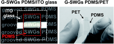
The PDMS film with G-SWGs in itself can be employed as a flexible and stretchable substrate. However, it can be also very useful as a protective antireflection layer in other transparent substrates or covers, which are utilized in optical and optoelectronic devices, due to its good and simple lamination and detachability. To demonstrate the applicability of PDMS films with G-SWGs, the optical performance of ITO glass and PET substrates laminated with the one-side G-SWGs (P380) PDMS film was studied. Fig. 6 shows the measured total (a) transmittance and (b) reflectance spectra of the ITO glass and PET with and without the one-side G-SWGs (P380) PDMS film and (c) the TAS value of the corresponding samples as a function of θin. As expected, the introduction of the G-SWGs PDMS film with the short period of 380 nm into the transparent ITO glass and PET substrates led to the enhancement of their transmittance, and thus their reflectivity was reduced over a wide wavelength region of 400–1100 nm, resulting in the increased TAT ≈ 86.8 and 95.1% and the decreased RAT ≈ 7.1 and 5.6% for the ITO glass and PET with the G-SWGs PDMS film, respectively (i.e., TAT ≈ 83.5 and 91.6% and RAT ≈ 10 and 8.9% for the bare ITO glass and PET, respectively). The antireflection property of the G-SWGs (P380) PDMS film is also verified from the photograph in the left inset of Fig. 6(b). The letters under the bare ITO glass (white-dotted line) are almost not seen because of the strongly reflected white fluorescent light at its both-side surfaces. On the other hand, the characters under the G-SWGs PDMS film (red-dotted line) attached on the ITO glass (i.e., G-SWGs PDMS/ITO glass) are relatively well seen due to its antireflection effect caused by the step gradient effective refractive index profile in the constituent materials of air (n = 1)/PDMS (1.43)/glass (1.5) or PET (1.65) and the tapered structure of the G-SWGs on the PDMS film.22,31 In addition, for the photograph in the right inset of Fig. 6(b), the flexibility and robustness of the G-SWGs PDMS film laminated on the PET (i.e., G-SWGs PDMS/PET) can be confirmed, and thus this architecture can be also used in various rigid and flexible optical systems. For the incident angle-dependent transmittance characteristics in Fig. 6(c), the samples laminated with the G-SWGs (P380) PDMS film showed larger TAS values at whole θin values of 10–70°.
image file: c6ra15499a-f6.tif
Fig. 6 Measured total (a) transmittance and (b) reflectance spectra of the ITO glass and PET substrates laminated with and without the one-side G-SWGs (P380) PDMS film. (c) Measured average specular transmittance (TAS) of the corresponding samples as a function of θin. The photographs of the G-SWGs (P380) PDMS film laminated on the ITO glass (left) and PET (right) substrates (i.e., G-SWGs PDMS/ITO glass and G-SWGs PDMS/PET) to demonstrate its antireflection and flexibility/robustness are also shown in the inset of (b).

Surface wetting properties

Finally, for practical outdoor environment applications, the surface wetting properties of the PDMS films with the G-SWGs (P380) before and after FOTS treatments were investigated in Fig. 7, including the photographs of the water droplets on the corresponding samples. For comparison, the water contact angle of the flat PDMS film was also characterized. As shown in Fig. 7(a), the flat PDMS film had a hydrophobic surface with a water contact angle (WCA) value of ∼98°. On the other hand, by integrating the G-SWGs (P380) on the PDMS surface, the hydrophobicity was increased to a WCA value of ∼122°. This is due to the increased surface roughness, which can be explain by the Cassie–Baxter model.32 Furthermore, the G-SWGs PDMS film after the FOTS surface modification showed a further increased WCA value of ∼140°. As also shown in the photograph of Fig. 7(b), the water droplets on the surface of FOTS-treated G-SWGs (P380) PDMS film were kept to be a more closely sphere-like shape compared to the other samples (i.e., flat PDMS film and G-SWGs PDMS film before the FOTS treatment). This hydrophobic surface with a relatively large WCA value can conduct the self-cleaning function, which removes the surface pollutants like dusts by rolling down water droplets (e.g., rain). The self-cleaning ability would maintain the optical performance of outdoor systems for a long time.24 From these results, the polymer films with the G-SWGs surface can be widely used as highly-transparent protective cover-layers or substrates with multi-functionalities, such as antireflection/light scattering, thermal-resistance, and self-cleaning abilities, in a variety of optical and optoelectronic systems.
image file: c6ra15499a-f7.tif
Fig. 7 Photographs for (a) a water droplet on the surface of the flat PDMS film and the G-SWGs (P380) PDMS films before and after the FOTS treatment including each WCA value and (b) water droplets on the surface of the corresponding samples.

Conclusions

The incorporation of the G-SWGs, which were simply transferred from the Si molds with conical SWGs by the facile and cost-effective SIL method, into the surface of PDMS films enhanced the opical properties (i.e., antireflection and light scattering) of the bare PDMS film with a flat surface in wide ranges of light wavelengths (λ = 400–1100 nm) and angles (θin = 0–70°). The theoretically calculated transmittance results by the RCWA and FDTD simulations exhibited similar trends to the experimentally measured data. For their practical feasibility, the G-SWGs (P380) PDMS film was laminated onto the transparent ITO glass and PET substrates, leading to their increased transmission (or reduced surface reflection) of the corresponding substrates with the bare surface. Furthermore, the G-SWGs PDMS films showed the relatively good thermal durability at temperatures less than 180 °C and the high WCA value of ∼140°. These results suggest that thermal-tolerant G-SWGs PDMS films with efficient broadband and wide-angle antireflection, light-scattering, and self-cleaning abilities can be very useful for high performance of flexible and rigid optical and optoelectronic systems.

Acknowledgements

This work was supported by the National Research Foundation of Korea (NRF) grant funded by the Korea government (MSIP) (No. 2013R1A2A2A01068407).

References

  1. S. Salheim, E. Schäffer, J. Mlynek and U. Steiner, Science, 1999, 283, 520 CrossRef.
  2. V. E. Ferry, A. Polman and H. A. Atwater, ACS Nano, 2011, 5, 10055 CrossRef CAS PubMed.
  3. J. Zhu, C. M. Hsu, Z. Yu, S. Fan and Y. Cui, Nano Lett., 2010, 10, 1979 CrossRef CAS PubMed.
  4. Y. M. Song, S. J. Jang, J. S. Yu and Y. T. Lee, Small, 2010, 6, 984 CrossRef CAS PubMed.
  5. J. W. Leem, J. S. Yu, D. H. Jun, J. Heo and W. K. Park, Sol. Energy Mater. Sol. Cells, 2014, 127, 43 CrossRef CAS.
  6. K. Peng, Y. Xu, Y. Wu, Y. Yan, S. T. Lee and J. Zhu, Small, 2005, 1, 1062 CrossRef CAS PubMed.
  7. S. L. Diedenhofen, G. Vecchi, R. E. Algra, A. Hartsuiker, O. L. Muskens, G. Immik, E. P. A. M. Bakkers, W. L. Vos and J. G. Rivas, Adv. Mater., 2009, 21, 973 CrossRef CAS.
  8. J. Hiller, J. D. Mendelsohn and M. F. Rubner, Nat. Mater., 2002, 1, 59 CrossRef CAS PubMed.
  9. S. J. Jang, Y. M. Song, J. S. Yu, C. I. Yeo and Y. T. Lee, Opt. Lett., 2011, 36, 253 CrossRef CAS PubMed.
  10. R. Dewan, J. I. Owen, D. Madzharov, V. Jovanov, J. Hüpkes and D. Knipp, Appl. Phys. Lett., 2012, 101, 103903 CrossRef.
  11. Y. H. Ko and J. S. Yu, Opt. Express, 2011, 19, 15574 CrossRef CAS PubMed.
  12. J. W. Leem, Y. P. Kim and J. S. Yu, J. Opt. Soc. Am. B, 2012, 29, 357 CrossRef CAS.
  13. H. Choi, S. J. Ko, Y. Choi, P. Joo, T. Kim, B. R. Lee, J. W. Jung, H. J. Choi, M. Cha, J. R. Jeong, I. W. Hwang, M. H. Song, B. S. Kim and J. Y. Kim, Nat. Photonics, 2013, 7, 732 CrossRef CAS.
  14. K. Jung, H. J. Song, G. Lee, Y. Ko, K. Ahn, H. Choi, J. Y. Kim, K. Ha, J. Song, J. K. Lee, C. Lee and M. Choi, ACS Nano, 2014, 8, 2590 CrossRef CAS PubMed.
  15. S. I. Na, S. S. Kim, J. Jo, S. H. Oh, J. Kim and D. Y. Kim, Adv. Funct. Mater., 2008, 18, 3956 CrossRef CAS.
  16. U. Plachetcka, M. Bender, A. Fuchs, B. Vratzov, T. Glinsner, F. Lindner and H. Kurz, Microelectron. Eng., 2004, 73–74, 167 CrossRef.
  17. J. Orava, T. Kohoutek, A. L. Greer and H. Fudouzi, Opt. Mater. Express, 2011, 1, 796 CrossRef CAS.
  18. S. H. Ahn and L. J. Guo, ACS Nano, 2009, 3, 2304 CrossRef CAS PubMed.
  19. Y. M. Song, Y. Xie, V. Malyarchuk, J. Xiao, I. Jung, K. J. Choi, Z. Liu, H. Park, C. Lu, R. H. Kim, R. Li, K. B. Crozier, Y. Huang and J. A. Rogers, Nature, 2013, 497, 95 CrossRef CAS PubMed.
  20. F. Galeotti, F. Trespidi, G. Timò and M. Pasini, ACS Appl. Mater. Interfaces, 2014, 6, 5827 CAS.
  21. Y. H. Ko, S. H. Lee, J. W. Leem and J. S. Yu, RSC Adv., 2014, 4, 10216 RSC.
  22. J. W. Leem, S. Kim, S. H. Lee, J. A. Rogers, E. Kim and J. S. Yu, Adv. Energy Mater., 2014, 4, 1301315 CrossRef.
  23. Y. B. Park, H. Im, M. Im and Y. K. Choi, J. Mater. Chem., 2011, 21, 633 RSC.
  24. J. Son, S. Kundu, L. K. Verma, M. Sakhuja, A. J. Danner, C. S. Bhatia and H. Yang, Sol. Energy Mater. Sol. Cells, 2012, 98, 46 CrossRef CAS.
  25. J. W. Leem, Y. M. Song and J. S. Yu, Appl. Phys. B, 2010, 100, 891 CrossRef CAS.
  26. J. W. Leem, S. Kim, C. Park, E. Kim and J. S. Yu, ACS Appl. Mater. Interfaces, 2015, 7, 6706 CAS.
  27. Y. M. Song, H. J. Choi, J. S. Yu and Y. T. Lee, Opt. Express, 2010, 18, 13063 CrossRef CAS PubMed.
  28. J. W. Leem, M. S. Kim and J. S. Yu, J. Opt. Soc. Am. B, 2013, 30, 1665 CrossRef CAS.
  29. S. J. Wilson and M. C. Hutley, Opt. Acta, 1982, 29, 993 CrossRef.
  30. E. Hecht, Optics, Addison-Wesley, NY, USA, 4th edn, 2002, ch. 10 Search PubMed.
  31. P. B. Clapham and M. C. Hutley, Nature, 1973, 244, 281 CrossRef.
  32. A. B. D. Cassie and S. Baxter, Trans. Faraday Soc., 1944, 40, 546 RSC.

This journal is © The Royal Society of Chemistry 2016
Click here to see how this site uses Cookies. View our privacy policy here.