
Metal-to-insulator transition near room temperature in graphene oxide and graphene oxide + TiO2 thin films
G. H. Weghera,
E. R. Viana*a,
G. M. Ribeirob and
J. F. Deusa
aDepartamento Acadêmico de Física (DAFIS), Universidade Tecnológica Federal do Paraná (UTFPR), Av. Sete de Setembro, 3165, Rebouças CEP 80230-901, Curitiba, PR, Brazil. E-mail: emilsonjunior@utfpr.edu.br; Tel: +55-41-3310-4639
bDepartamento Física, Universidade Federal de Minas Gerais (UFMG), Av. Pres. Antônio Carlos, 6627 – Pampulha. CEP 31270-901, Belo Horizonte, MG, Brazil. Tel: +55-31-3409-5625
First published on 7th November 2016
Abstract
Thin films of graphene oxide (GO) and a composite of graphene oxide with titanium oxide (GO + TiO2) were prepared via an alternative chemical route based on Hummer's method. The morphology and crystalline structure of the GO and GO + TiO2 thin films were investigated by X-ray power diffraction (XRD) and scanning electron microscopy (SEM). Anatase TiO2 nanostructures were incorporated into the bulk and surface of GO. Ultraviolet-visible spectroscopy (UV-vis) and Fourier transform infrared spectroscopy (FTIR) were also performed in order to corroborate with the results obtained by XRD, SEM and TEM. The electrical characterization of GO and GO + TiO2 TFs was performed using the four-probe van der Pauw method from 400 K down to 77 K. The resistivity, carrier density and carrier mobility in the TFs were determined as a function of temperature. It was found that the conductivity and mobility increased with the incorporation of TiO2 on GO; however, the concentration of free-carriers decreased. The analysis of the temperature dependence of the resistivity also showed that both films present a metal-to-insulator transition (MIT) near room temperature, at 280 K and 260 K for GO and GO + TiO2, respectively. Thus, for temperatures near 300 K the carrier density, thermally induced in GO and GO + TiO2 thin films, is so high that both the systems suffer a Mott MIT, which increases the prospects of using these films in a novel class of electronics, spintronics and photonics.
Introduction
In order to explore the features of a material and to provide better materials for technological applications, an understanding of the electron transfer behavior is very important for developing electronic devices.Graphene oxide (GO) and reduced graphene oxide (rGO) have been widely studied in recent years because of their promising applications as energy storage devices,1–4 transistors5,6 sensors,7–10 and solar cells11–13 and for photocatalytical and photoelectrochemical processes.14–19 They are also relevant in the field of nanomedicine, for the degradation of estrogens20 and as a material for cellular imaging and drug delivery.21
The possible chemical exfoliation routes allow the large-scale production of GO, which is advantageous with respect to the usual graphene production methods.22–25
The conduction mechanism of GO is strongly dependent on its oxidation level; therefore, it can be considered as an insulator with tunable properties, or as a semiconductor, particularly in the case of rGO.5,26 Its structure contains hydroxyl and epoxide functional groups on the top and bottom of the sheet and carboxyl and carbonyl groups on the edges.5,24,26 The electronic properties of rGO are usually associated with the variable-range hopping (VRH) mechanism. However, due to the complexity of the rGO structure, some deviations from the VRH mechanism are found.
Titanium dioxide (TiO2) is a semiconductor that has been widely studied for several years due to its interesting electrical and optical properties,2,10,27–29 such as high refractive index, high dielectric constant, and excellent transmittance in the visible range.27–31 These properties make TiO2 an important material for optoelectronic devices such as gas sensors10,27,29,30 and solar cells.27,30,31
In this study, TiO2 was incorporated into GO during the chemical exfoliation of graphite, via a modified Hummer's method. Hybrid thin films were produced and the effect of TiO2 incorporation on GO was evaluated. TiO2 can promote an enhancement in the reduction of GO to rGO, thus improving its electrical conductivity.
Recently, hybrid materials made of carbon-based materials, due to their inherent high thermal conductivity,36–38 have been studied and developed for applications as electromagnetic wave absorbers.32–35
Experimental
Synthesis of GO and GO + TiO2
In order to evaluate the properties of GO, we added TiO2 to the synthesis of GO via the modified Hummer's method.39,40In a beaker placed in a water bath at 5 °C, 1000 mg of graphite powder (Synth®) were mixed with 750 mg of sodium nitrate NaNO3 (Aldrich) and 64 g of sulfuric acid H2SO4 (Vetec®). After 30 min of magnetic stirring, 4500 mg of potassium permanganate KMnO4 (Aldrich®) were gradually added. The mixture was allowed to stir for 3 days, and then 100 mL of a 10% aqueous H2SO4![[thin space (1/6-em)]](https://www.rsc.org/images/entities/char_2009.gif) :H2O solution were added and allowed to stir for 2 hours. Subsequently, 250 mL of a 10% aqueous solution of hydrogen peroxide H2O2 (Vetec®) were added and left to stir for 3 days to give a yellowish mass. The solution was filtered and the obtained product was dried in a vacuum oven for 24 h at 60 °C. The product was washed with 1 L of a 20% aqueous HCl solution (Vetec®), filtered, then washed with 1 L of deionized water and subsequently placed to dry in a vacuum oven for 24 hours at 60 °C. Finally graphene oxide (GO) was obtained as a powder.
:H2O solution were added and allowed to stir for 2 hours. Subsequently, 250 mL of a 10% aqueous solution of hydrogen peroxide H2O2 (Vetec®) were added and left to stir for 3 days to give a yellowish mass. The solution was filtered and the obtained product was dried in a vacuum oven for 24 h at 60 °C. The product was washed with 1 L of a 20% aqueous HCl solution (Vetec®), filtered, then washed with 1 L of deionized water and subsequently placed to dry in a vacuum oven for 24 hours at 60 °C. Finally graphene oxide (GO) was obtained as a powder.
For the GO + TiO2 nanocomposite the route was the same, other than the composition of the initial mixture. In a beaker placed in a water bath at 5 °C, 1000 mg of graphite powder (Synth®) were mixed with 1000 mg of titanium dioxide TiO2 (Aldrich), 1000 mg of sodium nitrate NaNO3 (Aldrich®) and 70 g of sulfuric acid (Vetec®). The further steps were identical to the ones previously described for GO. Finally, graphene oxide (GO) with TiO2 incorporated in the bulk and in the surface was obtained as a powder.
Sample characterization
The morphology of the samples was studied by scanning electron microscopy (SEM – Zeiss EVO® MA15) and transmission electron microscopy (TEM – JEOL JEM® 1200EX-II). Fig. 1 shows the SEM images for GO (Fig. 1(A)) and GO + TiO2 (Fig. 1(B)) films. Fig. 2 shows the TEM images for GO (Fig. 2(A)) and GO + TiO2 (Fig. 2(B)) films. Fig. 2(B) displays the incorporation of TiO2 into GO, seen as white crystals onto the surface of GO. TEM images were also observed in order to show that the incorporation of TiO2 into GO is not only on the surface, but also in the bulk, seen as black particles on top and inside of GO. The incorporation of TiO2 into GO is so intense/stable that even in an aqueous solution stirred for several days, or in an ultrasonic bath for several hours, no isolated particles of TiO2 were observed in the TEM grid, displayed only those attached to GO.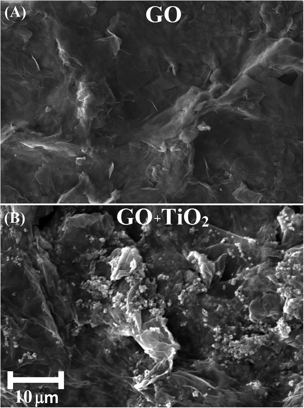 | ||
| Fig. 1 SEM images of GO (A) and GO + TiO2 (B) thin films. | ||
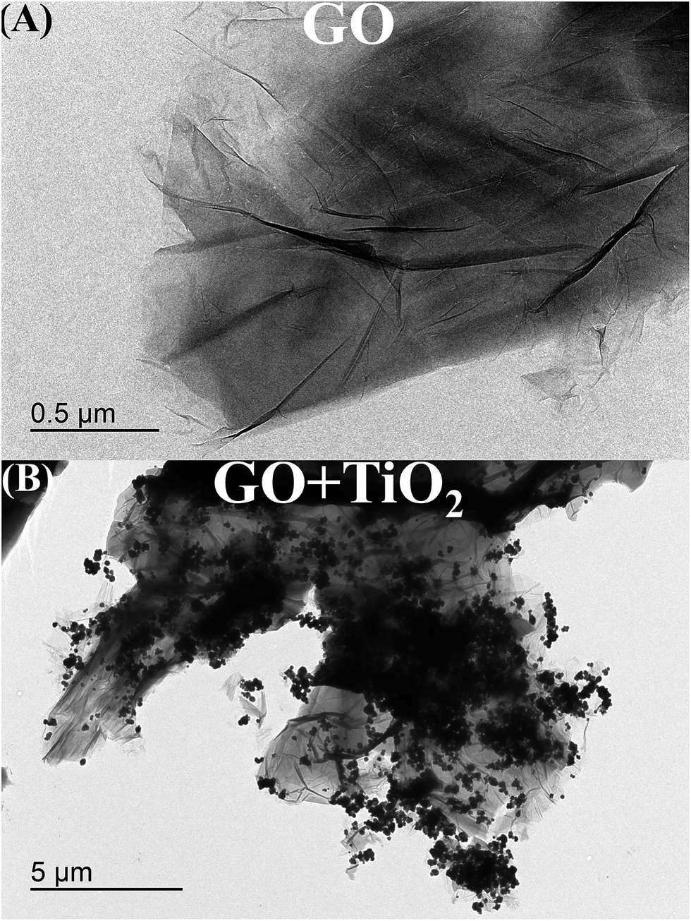 | ||
| Fig. 2 TEM images of GO (A) and GO + TiO2 (B) thin films. | ||
For the structural characterization, X-ray diffraction (XRD – Shimadzu XRD-700®) was performed to identify the crystallographic phases present in the samples. UV-vis absorbance (UV-vis) with a FEMTO 800-XI® spectrophotometer and Fourier transform infrared spectroscopy (FTIR) with a Varian 640-IR® spectrophotometer were also carried out.
Electrical characterization
In the present study, the electrical DC transport was measured using the van der Pauw method41 in order to reduce contact effects. The electrical transport properties of the samples were studied by measuring the Hall effect (with a Keithley® 7100 Hall effect card), and the electrical resistivity (Keithley® 7100 Hall effect card, Keithley® 196, Keithley® 220), in the dark and as a function of the temperature in the range of 77–400 K. The samples were measured inside a CF104 cryostat equipped with an ITC 503 Oxford® temperature controller.Results and discussion
XRD
Fig. 3 shows the XRD spectra of GO (black line) and GO + TiO2 (blue line) thin films. The GO spectra exhibits two peaks at 2θ ≈ 10.5° and 20°. The first peak is correlated to an interlayer spacing of 0.85 nm in the layer-like GO. The peak at 20° is broad and weak and is attributed to reduced graphene oxide, rGO.11 For GO + TiO2, zone axes (101), (103), (004), (112), (200), (105), (211), (204), (116), (301) and (215) were observed, corresponding to the anatase phase of TiO2.11 In the inset of Fig. 3, the UV-vis spectra of GO (black line) and GO + TiO2 (blue line) is shown. The GO spectrum exhibits a peak at 233 nm due to the π → π* transitions of aromatic C–C and C![[double bond, length as m-dash]](https://www.rsc.org/images/entities/char_e001.gif) C bonds, and a shoulder at 300 nm due to the n → π* transitions of CO bonds.42 GO–TiO2 shows absorbance intensity in the range of 240–450 nm with a peak at 350 nm, attributed to the strong absorption of TiO2, and a shoulder at 250 nm, indicating the interaction between TiO2 and GO.42
C bonds, and a shoulder at 300 nm due to the n → π* transitions of CO bonds.42 GO–TiO2 shows absorbance intensity in the range of 240–450 nm with a peak at 350 nm, attributed to the strong absorption of TiO2, and a shoulder at 250 nm, indicating the interaction between TiO2 and GO.42
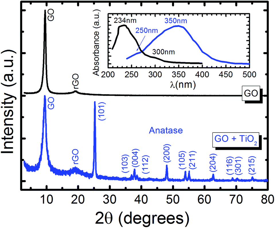 | ||
| Fig. 3 XRD patterns of GO (black) and GO + TiO2 (blue). In the inset, UV-vis absorption spectra of GO (black) and GO + TiO2 (blue) are displayed. | ||
FTIR
Fig. 4 shows the spectra for GO and GO + TiO2, obtained from the Fourier transform infrared spectroscopy (FTIR) studies. The GO spectrum shows a broad and intense band at 3000–3500 cm−1 (corresponding to the O–H stretching vibrations from hydroxyl groups43), 2984 cm−1 (C–H stretching vibrations44), 1729 cm−1 (CO stretching vibrations from carbonyl and carboxyl groups45), 1629 cm−1 (CC stretching vibrations, skeletal vibrations from non-oxidized graphene domains),46 1380 cm−1 (O–H stretching vibrations from hydroxyl groups),47 1227 cm−1 (C–OH stretching vibrations, breathing vibrations from epoxy groups48), and 1037 cm−1 (C–O stretching vibrations49). The GO + TiO2 spectrum shows the corresponding small displacements and a broad band between 600 and 1000 cm−1, characteristic of Ti–O stretching.50
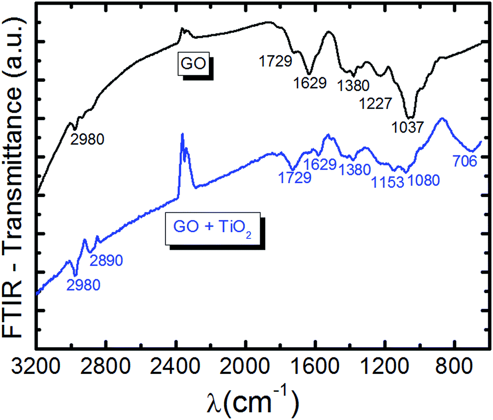 | ||
| Fig. 4 FTIR spectra of GO (black) and GO + TiO2 (blue). | ||
Variable range hopping (VRH) conduction
Fig. 5 shows the electrical resistivity ρ(T) of GO and GO + TiO2 TFs as a function of the temperature, between 77 K and 400 K. Kaiser49 and Joung51 already reported that electrical conduction in rGO can be explained by Mott variable-range hopping (Mott-VRH) between localized states. In the 2D Mott-VRH model the temperature dependence of the conductivity can be described as follows:52,53
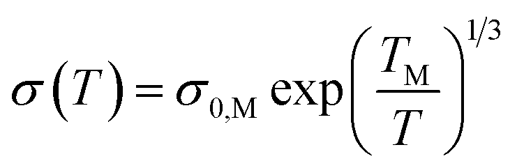 | (1) |
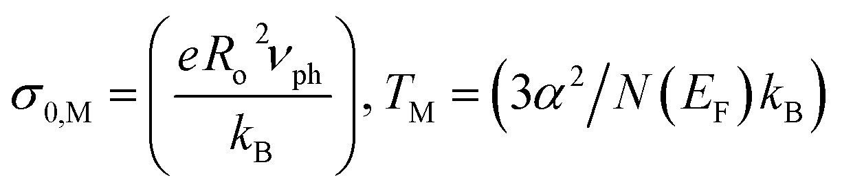 | (2) |
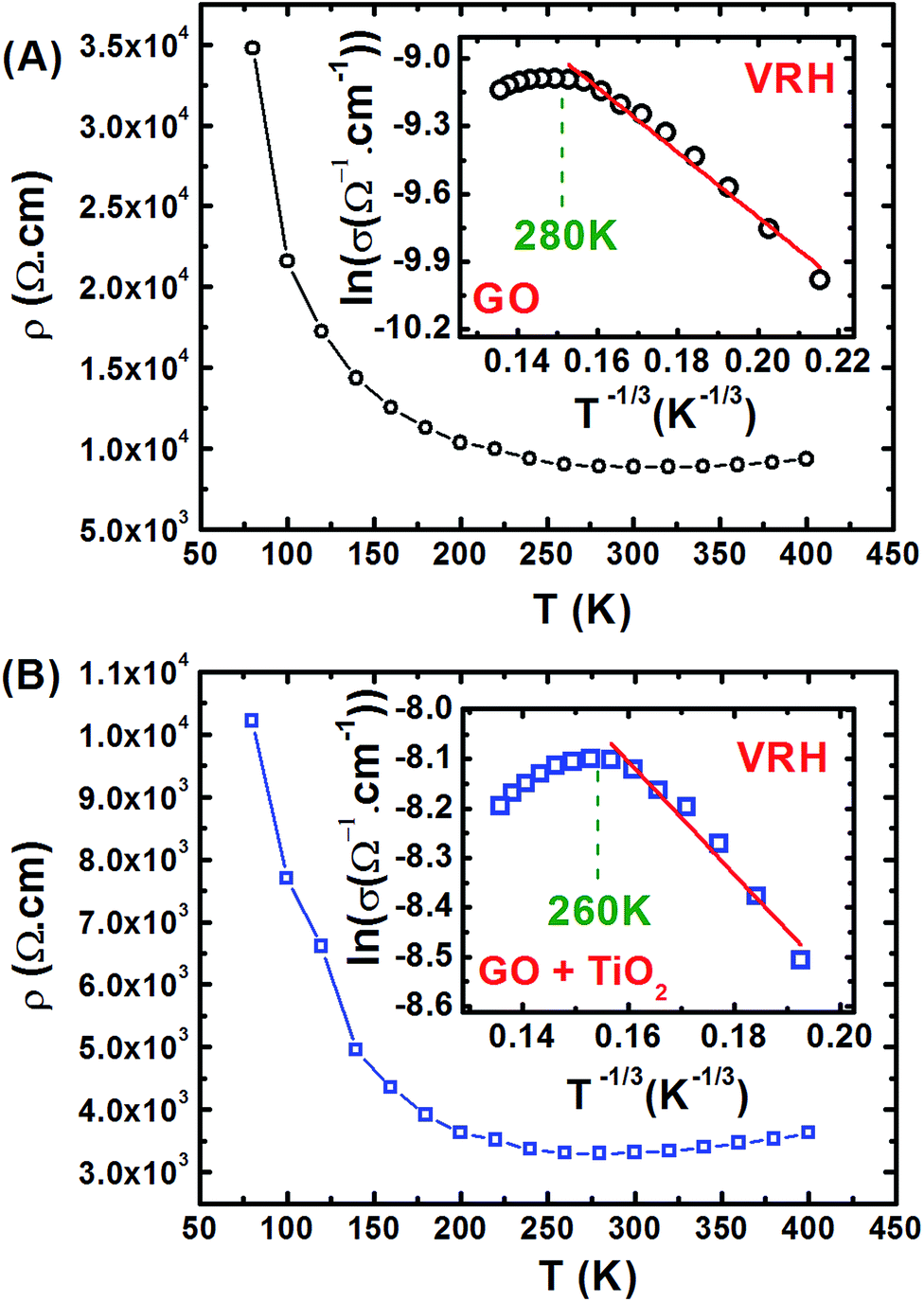 | ||
| Fig. 5 Temperature dependence of the electrical resistivity ρ(T) for (A) GO, and (B) GO + TiO2 thin films. In the inset, Arrhenius plot showing the metal to insulator transition at 280 K and 260 K for GO and GO + TiO2, respectively is displayed. The red lines correspond to the fitting of the experimental data using eqn (1). | ||
In the inset of Fig. 5, we show the VRH plot of ln(σ) vs. T−1/3 in the temperature range of 280–100 K for GO (Fig. 5(A)) and 260–140 K for GO + TiO2 (Fig. 5(B)). The red lines correspond to the fitting of the experimental data using eqn (1). A summary with the most important obtained hopping parameters is presented in Table 1.
| Sample | σ0,M (10−5 Ω cm−1) | TM (103 K) | N(EF) (1013 cm−2/eV) | Ro (nm) | nMIT (1019 cm−3) |
|---|---|---|---|---|---|
| GO | 1.695 | 4.607 | 18.8 | 0.164 | 2.831 |
| GO + TiO2 | 1.855 | 1.454 | 60.0 | 0.172 | 2.474 |
Metal to insulator transition – MIT
The Bohr radius can be assigned as an estimate for the length of the localized states, and can be calculated by:| aBohr = (4πεhc2/m*e2) | (3) |
The value obtained for the Bohr radius (0.159 nm) is very close to the optimum hopping distance obtained for GO and GO + TiO2, which is 0.164 and 0.172 nm, respectively. This result can indicate that both GO and GO + TiO2 could have very similar MIT temperatures, which experimentally can be observed at 280 K for GO and at 260 K for GO + TiO2.
Mott55 pointed out that a system suffers a metal to insulator transition when the electrons are in a narrow band, for which the orbitals can be described by the tight-binding method as consisting of atomic wave functions. The critical carrier density (nMIT) at which a MIT should take place can be determined by the following equation:55
| (nMIT)1/3aBohr = const. | (4) |
If we consider the optimum hopping distance as the localization length of the defects, we can estimate the critical density of defects nMIT for each sample, using aBohr = Ro in eqn (4). For GO we expected a MIT transition of approximately 2.8 × 1019 cm−3, and for GO + TiO2 at 2.5 × 1019 cm−3. Experimentally, the MIT transition occurs at 280 K and 260 K for GO and GO + TiO2, or at carrier densities of 7.52 × 1020 cm−3 or 5.6 × 1020 cm−3, respectively.
Due to the existence of a near room temperature metal to insulator transition, GO and GO + TiO2 are potential candidates for a novel class of electronics and photonics applications, such as field effect switches, memristive devices, electronic oscillators and spintronics.56
The presence of a Mott MIT is also an indication that at a lower temperature range (above 77 K) it is expected that GO and GO + TiO2 would undergo a transition from Mott-VRH to Efros–Shklovskii VRH conduction, when the Coulomb gap (soft gap) that cannot be neglected appears in the density of states, at the Fermi level.57
In order to better understand the transport properties of GO and GO + TiO2, Hall effect measurements were performed at the same temperature range. Fig. 6(A) shows the free carrier density nHall as a function of the temperature. The nHall is of the order of 1020 cm−3 for both materials, although throughout the temperature range the carrier density in GO was higher than in GO + TiO2. The free carrier mobility μHall is given by the following equation:
| σ(T) = nHallμHalle → μHall = [qoρnHall]−1 | (5) |
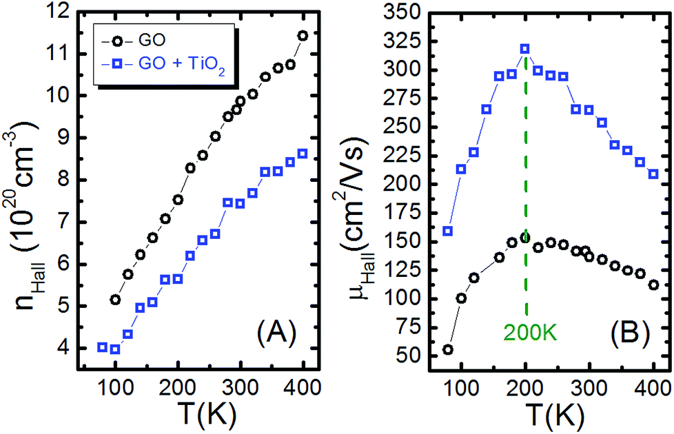 | ||
| Fig. 6 The temperature dependence of the (A) free carrier density nHall(T) and (B) free carrier mobility μHall(T), for GO (black dots) and for GO + TiO2 (blue dots). | ||
Fig. 6(B) shows the free carrier mobility nHall as a function of the temperature μHall(T). Throughout the temperature range the carrier mobility in GO + TiO2 was higher than in GO. For highly doped semiconductors (metal-like), the mobility increases as the temperature drops due to a reduction in electron–electron scattering. However, GO exhibits the opposite trend, due to a reduction in electron-lattice scattering, and we expected a decrease of the mobility as the temperature dropped.58 In Table 2 there is a summary of the electrical parameters for the GO and GO + TiO2 thin films.
| Sample | t (nm) | TMIT (K) | pmáx,400 K (1020 cm−3) | μmáx,200 K (cm2 V−1 s−1) |
|---|---|---|---|---|
| GO | 723 | 180 | 11.4 | 153 |
| GO + TiO2 | 980 | 160 | 8.6 | 318 |
Conclusions
In conclusion, we show a comparative study between graphene oxide (GO) and graphene oxide–titanium oxide (GO + TiO2) composite thin films prepared by a modified Hummer's method. XRD, FTIR and UV-vis absorption showed that the incorporation of TiO2 on GO was successful. Electrical characterization of the materials was carried out and the temperature dependence of the resistivity ρ(T), carrier density nHall(T) and carrier mobility μHall(T) was determined for the films. The GO film presented a higher carrier density and resistivity, and consequently a lower mobility than that of the GO + TiO2 film. The analysis of the temperature dependence of the resistivity also showed that both films present a near room temperature metal-to-insulator transition (MIT), at 280 K and 260 K for GO and GO + TiO2, respectively. Thus, for temperatures near 300 K the thermally induced carrier density in the films is so high that both systems suffer a Mott MIT transition. The presence of a near room temperature MIT makes GO and GO + TiO2 potential candidates for a novel class of electronics and photonics applications, such as field effect switches, memristive devices, electronic oscillators and spintronics.Acknowledgements
The authors would like to acknowledge the “Centro Multi-usuário de Caracterização de Materiais – CM2 (UTFPR)”, “Centro de Microscopia Eletrônica – CME (UFPR)”, Prof. Dr Julio Cesar Klein das Neves, Prof. Dr Joao Batista Floriano and Alexandre José Gonçalves of Universidade Tecnológica Federal do Paraná for providing the equipment and technical support for experiments involving SEM, TEM microscopy and XRD, UV-vis and FTIR measurements. The financial support of the Brazilian funding agencies CAPES, CNPq, FAPEMIG and Fundação Araucária is also acknowledged.References
- K. Pal, V. Panwar, S. Bag, J. Manuel, J.-H. Ahn and J. K. Kim, RSC Adv., 2015, 5, 3005–3010 RSC.
- Y. Ye, P. Wang, H. Sun, Z. Tian, J. Liu and C. Liang, RSC Adv., 2013, 5, 45038–45043 RSC.
- X. Li, C. Zhang and T. Meng, RSC Adv., 2016, 6, 4321–4328 RSC.
- Y. Ye, P. Wong, H. Sun, Z. Tian, J. Liu and C. Liang, RSC Adv., 2015, 5, 45038–45043 RSC.
- S. M. Jilani and P. Banerji, ACS Appl. Mater. Interfaces, 2014, 6, 16941–16948 CAS.
- I. Karteri, S. Karataş and F. Yakuphanoğlu, Appl. Surf. Sci., 2014, 318, 74–78 CrossRef CAS.
- Z. Ye, H. Tai, T. Xie, Y. Su, Z. Yuan, C. Liu and Y. Jiang, Mater. Lett., 2016, 165, 127–130 CrossRef CAS.
- D. Zhang, F. Jing, F. Gao, L. Shen, D. Sun, J. You, Y. Chen and S. Ruan, RSC Adv., 2015, 5, 83795–83800 RSC.
- B. Chitara, L. S. Panchakarla, S. B. Krupanidhi and C. N. R. Rao, Adv. Mater., 2011, 23, 5419–5424 CrossRef CAS PubMed.
- J. Zhang, C. Zhao, P. A. Hu, Y. Q. Fu, Z. Wang, W. Cao, B. Yang and F. Placido, RSC Adv., 2015, 3, 22185–22190 RSC.
- M. Horn, C. F. Schwerdtfeger and E. P. Meagher, Zeitschrift für Kristallographie, 1972, 136, 273–281 CrossRef CAS.
- A. Morais, J. P. C. Alves, F. A. S. Lima, M. L. Cantu and A. F. Nogueira, J. Photonics Energy, 2015, 5, 057408 CrossRef CAS.
- T. Umeyama, D. Matano, J. Baek, S. Gupta, S. Ito, V. R. Subramanian and H. Imahori, Chem. Lett., 2015, 44, 1410–1412 CrossRef CAS.
- D. Kong, M. Zhao, S. Li, F. Huang, J. Song, Y. Yuan, Y. Shen and A. Xie, Nano, 2016, 11, 60–68 Search PubMed.
- A. Morais, C. Longo, J. R. Araujo, M. Barroso, J. R. Durrant and A. F. Nogueira, Phys. Chem. Chem. Phys., 2016, 18, 2608 RSC.
- R. He and W. He, Ceram. Int., 2016, 42, 5766–5771 CrossRef CAS.
- N. Seifvand and E. Kowsari, RSC Adv., 2016, 6, 4321–4328 RSC.
- Z. Lu, G. Chen, W. Hao, G. Sun and Z. Li, RSC Adv., 2015, 5, 72916–72922 RSC.
- S. Chowdhury, G. K. Parshetti and R. Balasubramanian, Chem. Eng. J., 2015, 263, 374–384 CrossRef CAS.
- Y. Yang, L. Luo, M. Xiao, H. Li, X. Pan and F. Jiang, Mater. Sci. Semicond. Process., 2015, 40, 183–193 CrossRef CAS.
- J. Liu, L. Cui and D. Losic, Acta Biomater., 2013, 9, 9243–9244 CrossRef CAS PubMed.
- S. Lee, S. H. Eom, J. S. Chung and S. H. Hur, Chem. Eng. J., 2013, 233, 297–304 CrossRef CAS.
- M. Zhang, B. Gao, D. C. Vanegas, E. S. McLamore, J. Fang, L. Liu, L. Wu and H. Chen, Chem. Eng. J., 2014, 243, 340–346 CrossRef CAS.
- L. Stobinski, B. Lesiak, A. Malolepszy, M. Mazurkiewicz, B. Mierzwa, J. Zemek, P. Jiricek and I. Bieloshapka, J. Electron Spectrosc. Relat. Phenom., 2014, 195, 145–154 CrossRef CAS.
- C. Wu, J. Jiu, T. Araki, H. Koga, T. Sekitani, H. Wang and K. Suganuma, RSC Adv., 2016, 6, 15838–15845 RSC.
- D. H. Ha, S. Jung, H.-J. Kim, D. Kim, W.-J. Kim, S. N. Yi, Y. Jun and Y. J. Yun, Synth. Met., 2015, 204, 90–94 CrossRef CAS.
- Y. R. Park and K. J. Kim, Thin Solid Films, 2005, 484, 34–38 CrossRef CAS.
- S.-H. Jeong, B.-S. Kim, B.-T. Lee, H. R. Park and J.-K. Kim, J. Korean Phys. Soc., 2002, 41, 67–72 CAS.
- S. Vyas, R. Tiwary, K. Shubham and P. Chakrabarti, Superlattices Microstruct., 2015, 80, 215–221 CrossRef CAS.
- Z. Wang, U. Helmersson and P.-O. Käll, Thin Solid Films, 2002, 405, 50–54 CrossRef CAS.
- C. R. Tubío, F. Guitián, J. R. Salgueiro and A. Gil, Mater. Lett., 2015, 141, 203–206 CrossRef.
- X. Li, J. Feng, H. Zhu, C. Qu, J. Bai and X. Zheng, RSC Adv., 2014, 4, 33619–33625 RSC.
- X. Zheng, J. Feng, Y. Zong, H. Miao, X. Hu, J. Bai and X. Li, J. Mater. Chem. C, 2015, 3, 4452–4463 RSC.
- X. Li, J. Feng, Y. Du, J. Bai, H. Fan, H. Zhang, Y. Peng and F. Li, J. Mater. Chem. A, 2015, 3, 5535–5546 CAS.
- J. Feng, F. Pu, Z. Li, X. Li, X. Hu and J. Bai, Carbon, 2016, 104, 214–225 CrossRef CAS.
- J. Gu, C. Liang, J. Dang, W. Dong and Q. Zhang, RSC Adv., 2016, 6, 35809–35814 RSC.
- J. Gu, N. Li, L. Tian, Z. Lv and Q. Zhang, RSC Adv., 2015, 5, 36334–36339 RSC.
- J. Gu, X. Yang, Z. Lv, N. Li, C. Liang and Q. Zhang, Int. J. Heat Mass Transfer, 2016, 92, 15–22 CrossRef CAS.
- C. Xiang, M. Li, M. Zhi, A. Manivannan and N. Wu, J. Mater. Chem., 2012, 22, 19161 RSC.
- M. Acik and S. Darling, J. Mater. Chem. A, 2016, 4, 6185–6235 CAS.
- D. C. Look, Electrical Characterization of GaAs Materials and Devices, Wiley, New York - NY, 1989 Search PubMed.
- A. Morais, J. P. C. Alves, F. A. S. Lima, M. Lira-Cantu and A. F. Nogueira, J. Photonics Energy, 2015, 5, 057408 CrossRef CAS.
- S. M. Jilani and P. Banerji, ACS Appl. Mater. Interfaces, 2014, 6, 16941–16948 CAS.
- I. Karteri, S. Karatas and F. Yakuphanoglu, Appl. Surf. Sci., 2014, 318, 74–78 CrossRef CAS.
- D. H. Ha, S. Jung, H. J. Kim, D. Kim, W. J. Kim, S. N. Yi, Y. Jun and Y. J. Yun, Synth. Met., 2015, 204, 90–94 CrossRef CAS.
- I. Jung, D. A. Dikin, R. D. Piner and R. S. Ruoff, Nano Lett., 2008, 8, 4283–4287 CrossRef CAS PubMed.
- G. Eda, C. Mattevi, H. Yamaguchi, H. Kim and M. Chhowalla, J. Phys. Chem. C, 2009, 113, 15768–15771 CAS.
- H. J. Kim, D. Kim, S. Jung, S. N. Yi, Y. J. Yun, S. K. Chang and D. H. Há, J. Phys. Chem. C, 2015, 119, 28685–28690 CAS.
- A. B. Kaiser, C. G. Gomes-Navarro, R. S. Sundaram, M. Burghard and K. Kern, Nano Lett., 2009, 9, 1787–1792 CrossRef CAS PubMed.
- H. Yoo, Y. Kim, J. Lee, H. Lee, Y. Yoon, G. Kim and H. Lee, Chem.–Eur. J., 2012, 18, 4923–4929 CrossRef CAS PubMed.
- D. Joung and S. I. Khondaker, Phys. Rev. B: Condens. Matter Mater. Phys., 2012, 86, 235423 CrossRef.
- N. F. S. Mott, Conduction in Non-Crystalline Materials, Clarendon Press, Oxford, 1993 Search PubMed.
- B. I. Shklovskii and A. L. Efros, Electronic Properties of Doped Semiconductors, Springer-Verlag, Berlin, 1984 Search PubMed.
- F. C. Salomão, E. M. Lanzoni, C. A. Costa, C. Deneke and E. B. Barros, Langmuir, 2015, 31, 11339–11343 CrossRef PubMed.
- N. F. Mott, Rev. Mod. Phys., 1968, 40, 667 CrossRef.
- Z. Yang, C. Ko and S. Ramanathan, Annu. Rev. Mater. Res., 2011, 41, 337–367 CrossRef CAS.
- E. R. Viana, J. C. Gonzalez, G. M. Ribeiro and A. G. de Oliveira, Phys. Status Solidi RRL, 2012, 6, 262–264 CrossRef CAS.
- H. Seo, S. Ahn, J. Kim, Y. A. Lee, K. H. Chung and K. J. Jeon, Sci. Rep., 2014, 4, 5642 CAS.
| This journal is © The Royal Society of Chemistry 2016 |