DOI:
10.1039/C6RA14124B
(Paper)
RSC Adv., 2016,
6, 86770-86781
Development of Al-doped ZnO thin film as a transparent cathode and anode for application in transparent organic light-emitting diodes†
Received
31st May 2016
, Accepted 26th August 2016
First published on 26th August 2016
Abstract
Aluminum doped zinc oxide thin films have been prepared by sputtering under argon gas pressure of 0.15 Pa at different radio frequency (RF) power densities to optimize the conditions for application in both bottom emitting and transparent OLEDs. The films exhibit a wurtzite-type hexagonal structure with the [0001] preferred orientation and optical transmittance of better than 80% in the visible region, but, varying energy bandgap. The sputtering at a high RF power density of 2.47 W cm−2 yields Al–ZnO films of minimum resistivity (∼1 × 10⁻³ Ω cm) and high work function (∼4.44 eV), appropriate for the anode in bottom emitting OLEDs. On the other hand, AZO films obtained at the low RF power density of 0.31 W cm−2 correspond to a low work function (3.90 eV) with slightly higher electrical resistivity (5.60 × 10⁻³ Ω cm), useful for cathodes in transparent OLEDs. The comparable performance observed for OLEDs fabricated with AZO and ITO anodes demonstrates the suitability of AZO as an alternative electrode. The increase in RF power density during sputtering leads to perceptible damage of the organic layer. The introduction of a buffer layer of Alq3/LiF/Al just above the organic layer is shown to suppress the damages significantly and improve the performance of the transparent OLEDs.
1. Introduction
Organic light-emitting diodes (OLEDs) have found applications in flat panel displays and solid state lighting applications. They can be classified as bottom emitting or transparent OLEDs, depending on the emission occurring from the anode, or both (anode and cathode) ends.1 Mg–Ag alloy and double (Li:Al) layers are typically used as the cathode. LiF or Cs2CO2 is also introduced sometimes between the cathode (Al) and electron transport layer (ETL) for better electron injection efficiency.2 Indium tin oxide is a known anode material for efficient hole injection. Its work function is high (4.5–4.6 eV) and can be further improved by oxygen plasma treatment.3,4
The transparent OLEDs emitting light from both sides have applications in double-sided (or head-up) displays and smart windows. Gu et al.5 fabricated transparent OLEDs using ITO as the anode (or bottom electrode) and a thin layer (thickness ∼ 5–40 nm) of Mg–Ag alloy coated ITO as the cathode (or top electrode). Zhou et al.6 produced an inverted transparent OLED based on ITO at the bottom as the cathode and a semi-transparent gold film on top of the organic layer as the anode for hole injection. Lim et al.7 used a semi-transparent conducting and Cs/Al/Ag protected ITO as the cathode and Ag/ITO as the anode to get a transparent OLED. The semi-transparent film was employed to protect the organic layer from the irradiation of high energy species during the deposition of ITO by sputtering. Several transparent cathode materials with a conducting protecting layer, developed over the years, include CuPc/ITO, Li/BCP/ITO, Bphen:Li/ITO, Ag/ITO and Ca/ITO.8–11 Obviously, ITO is a crucial material for the display industry due to its high optical transmittance and low electrical resistivity. However, it contains indium, which is toxic, scarce, chemically unstable in reduced environments, and expensive. It can even diffuse to the organic layer causing degradation of OLEDs.12 This fact and the ever increasing demand of the industry, require the replacement of ITO by some inexpensive transparent conducting oxide (TCO). In particular, Al-doped ZnO (abbreviated as AZO) is often considered as a good substitute for ITO due to its abundance, high transparency in the visible range, thermal stability, non-toxic nature, and low cost.13 As anode for the bottom-emitting OLEDs, AZO thin films are usually grown above 150 °C by a variety of methods, viz., pulsed laser deposition (PLD),14 atomic layer deposition (ALD),15 plasma enhanced metal–organic chemical vapor deposition (PE-MOCVD),16 and sputtering (DC and RF).17,18 For example, Jha et al.19 prepared AZO thin films of various thicknesses (305–800 nm) at high substrate temperature (350 °C) and obtained a minimum electrical resistivity of 1.21 × 10⁻³ Ω cm with optical transparency of ∼86% for 805 nm thick films. Han et al.20 prepared the AZO thin films under various ambient gases (Ar, Ar + O2, and Ar + H2) at 300 °C to investigate the influence of the ambient gases and the flow rates of oxygen and hydrogen on the electrical and optical characteristics to test their suitability for anode material in OLEDs. The film prepared in ambient Ar + H2 exhibited a minimum resistivity of ∼3 × 10⁻³ Ω cm and optical transmittance of 85% in the visible region. Tseng et al.21 studied the thickness dependent electrical and optical properties of AZO thin films prepared on unheated (30–60 °C) and heated (250 °C) substrates. The AZO films with heated substrates exhibited the lowest electrical resistivity of 4.15 × 10⁻³ Ω cm and average optical transmittance of ∼92% in the visible region for thick films (706.3 nm). You et al.22 prepared AZO thin film (thickness ∼ 200 nm) by the pulsed laser co-ablation method and annealed at 450 °C in a mixed gas (5% H2 + 95% N2) for 1 h to realize electrical resistivity of 7.54 × 10⁻⁴ Ω cm. Also, Ga-doped and gallium and aluminium co-doped zinc oxide (GAZnO) films, usually prepared at higher substrate temperatures (>150 °C), are considered as alternative to ITO.23–30 However, the deposition of the transparent conducting cathode over the organic layer in transparent OLEDs has to be processed at relatively low temperatures (i.e., below 80 °C) and low RF power density to avoid degradation of the organic layer. Therefore, RF sputtering is preferred because of simplicity, having better process control, and providing an optimum deposition rate to yield smoother film over a large area at a low substrate temperature. Of course, the AZO material is not new and can replace ITO. Also, sputtering is the traditional method to produce films for TCO applications. While AZO films have largely been deposited above 150 °C to obtain desired electrical and optical properties, limited reports exist31 with the use of low substrate temperatures for their production to replace ITO as the anode in solar cells and OLEDs. This is a challenging task and vital for the application of AZO films as the anode in flexible opto-electronic devices and as cathodes in transparent OLEDs. Hence, an attempt is made here to deposit AZO thin films at ∼75 °C by sputtering with different RF power densities to ascertain their suitability as anode and cathode materials for OLED applications. Both bottom and transparent OLEDs based on AZO and commercial ITO electrodes have been fabricated and compared in terms of their characteristics.
2. Experimental details
AZO thin films were deposited on RCA cleaned, air dried, and ozone treated (for 20 min) glass substrates by RF sputtering using a ZnO![[thin space (1/6-em)]](https://www.rsc.org/images/entities/char_2009.gif) :Al2O3 (98:2 wt%) target of 99.99% purity procured from Kurtz J Lesker, USA. The substrates were mounted in a holder and held 7 cm away from the target. The chamber was initially evacuated to a base pressure of ∼2 × 10⁻⁶ mbar and then argon gas was introduced to maintain a pressure of 0.15 Pa. The deposition was undertaken at RF power density of 0.31, 0.62, 1.23, 1.85, and 2.47 W cm−2; the rates of deposition being 0.1, 0.5, 1.5, 2.3, and 3 Å s−1, respectively. The film thickness (∼400 nm) was controlled by a digital monitor and measured later with a Stylus profiler (Dektak 6M). The substrate was initially held at 25 °C, but its temperature increased to a maximum of 75 °C during the deposition of films of 400 nm thickness. A thermocouple was placed inside the working chamber to measure the temperature. The substrate temperature was displayed on a digital temperature indicator.
:Al2O3 (98:2 wt%) target of 99.99% purity procured from Kurtz J Lesker, USA. The substrates were mounted in a holder and held 7 cm away from the target. The chamber was initially evacuated to a base pressure of ∼2 × 10⁻⁶ mbar and then argon gas was introduced to maintain a pressure of 0.15 Pa. The deposition was undertaken at RF power density of 0.31, 0.62, 1.23, 1.85, and 2.47 W cm−2; the rates of deposition being 0.1, 0.5, 1.5, 2.3, and 3 Å s−1, respectively. The film thickness (∼400 nm) was controlled by a digital monitor and measured later with a Stylus profiler (Dektak 6M). The substrate was initially held at 25 °C, but its temperature increased to a maximum of 75 °C during the deposition of films of 400 nm thickness. A thermocouple was placed inside the working chamber to measure the temperature. The substrate temperature was displayed on a digital temperature indicator.
An X-ray diffractometer (Thermo Electron model ARL X'TRA), an atomic force microscope (Molecular Imaging Pico-SPM), Ocean optic fiber spectrometer model USB 2000, and a four-point probe were employed for phase identification, surface morphology, optical absorption, and sheet resistance measurements, respectively. Carrier concentrations of AZO thin films were determined by Hall effect data. The photoluminescence (PL) was recorded with the Edinburgh Steady state Fluorimeter FS920 to reveal the nature of the defects present. The work function was deduced through contact potential difference measurements undertaken with a Kelvin probe-7.
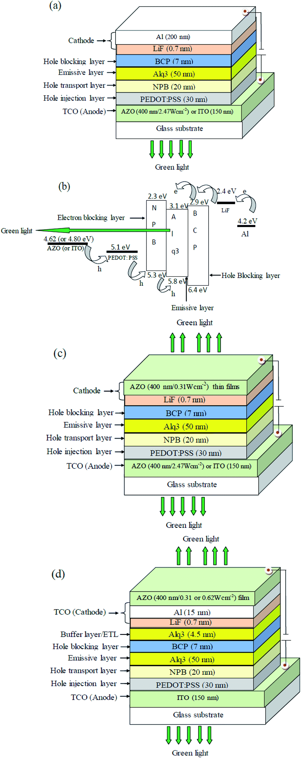
The AZO films deposited with RF power density of 0.62 and 2.47 W cm−2 served as transparent conducting anodes for the fabrication of the OLEDs (bottom emission type) with the process of Zhou et al.32 The patterning was realized by photolithography, using a shadow mask of size 4 mm × 30 mm. The patterned films were then cleaned gently with tissue paper (dipped in trichloroethylene and acetone) before boiling in isopropyl alcohol for 20 min and treating in ozone for 20 min to remove the organic impurities and increase the work function. A hole injection layer (thickness of ∼50 nm) of poly(3,4-ethylenedioxy-thiophene) poly(styrenesulphonate) (PEDOT:PSS) was subsequently spin coated at 2000 rpm over the AZO films. A 20 nm thin hole transport layer (HTL) of N,N-di(naphth-2-yl)-N,N′-di phenylbenzidine (NPB), a 50 nm thick green color electron emissive layer (EML) of tris(8-hydroxy-quinolinolato) aluminum(III) (Alq3) and a 7 nm thin hole blocking layer (HBL) of 2,9-di-methyl-4,7-diphenylphenanthroline (BCP) were deposited in conjunction by thermal evaporation in vacuum of ∼10−6 mbar. Finally, a bilayer of LiF and Al (thickness of ∼0.7 nm and 200 nm, respectively) was thermally laid under vacuum of ∼2 × 10⁻⁶ mbar over the BCP layer, using a mask (8 mm wide × 30 mm long slits), to act as the cathode. The structure of the device fabricated with active emission area of 8 mm × 4 mm is shown schematically in Fig. 1(a). For comparative study, another OLED (area of ∼8 mm × 5 mm) was fabricated with the commercial ITO thin films (5 mm wide × 30 mm long pattern size). For transparent OLEDs, LiF/AZO and Alq3/LiF/Al/AZO structures were laid on top of the BCP layer (Fig. 1(c) and (d)). The deposition of LiF or Alq3/LiF/Al layer(s) was made by thermal evaporation in vacuum of ∼2 × 10⁻⁶ mbar and of AZO by sputtering under argon pressure of 0.15 Pa with RF power density of 0.31 and 0.62 W cm−2. The thickness of LiF, Alq3, Al and AZO films were fixed at 0.7, 4.5, 15, and 400 nm, respectively. The OLEDs were analysed for their current density–voltage–luminance (J–V–L) characteristics with a Keithley Source Measure Unit (SMU) and a Minolta Spectroradiometer (CS-1000A). Also, capacitance–voltage (C–V) measurements of bottom OLEDs were made using an impedance analyzer (Agilent 4294 A).
 |
| | Fig. 1 Schematic of OLEDs: (a, b) bottom-type with its energy level diagram and (c, d) transparent-type. | |
3. Results and discussion
3.1. Structure, morphology and composition
The XRD pattern of the AZO thin films deposited at RF power density of 0.31 W cm−2 corresponds to a wurtzite-type hexagonal structure with the [0001] preferred orientation, i.e., the c-axis is perpendicular to the substrate (Fig. 2).33 Notice that the 0002 diffraction peak becomes progressively stronger, shifts towards a higher Bragg angle (2θ) as the RF power density used for film preparation increases, and reaches 2θ = 34.241° with highest intensity at 1.85 W cm−2. However, the films produced at power density of 2.47 W cm−2 depict the 0002 diffraction peak at a lower angle (2θ = 34.181°) with relatively poor intensity. These results suggest improvement in the crystallinity of films, only when the RF power density employed for deposition increases from 0.31 to 1.85 W cm−2. Also, the c-parameter decreases with the improvement of crystallinity in AZO films. At higher RF power density, film damage occurs and the lattice parameter increases slightly.34,35 The optimum RF power density for sputtering seems to be ∼1.85 W cm−2 for producing AZO films of wurtzite-type hexagonal structure, the [0001] preferred orientation and c-parameter of 5.233 Å ± 0.001 Å. The average crystallite size (D) as deduced from the Scherrer formula (D = 0.9λ/βcosθ, where λ is the X-ray wavelength = 1.5406 Å, β is the full width at half maximum of the diffraction peak at a Bragg angle θ after correction for instrumental broadening using a standard silicon sample) lies in the range 23–29 nm in sputtered AZO films at RF power densities of 0.31, 0.62, 1.23, 1.85, and 2.47 W cm−2. Table 1 lists the Bragg angles, full width at half maximum data, and the c-parameter of various AZO films, along with the RF power density used. Clearly, the 0002 peak shifts to a higher Bragg angle (2θ) with increasing the RF power density from 0.31 to 1.85 W cm−2. This indicates that the adjacent (0002) interplanar distance of AZO films decreases with the increase in RF power density from 0.31 to 1.85 W cm−2. This may be related to more aluminum (Al) atoms substituting for zinc (Zn) in the ZnO matrix, since the ionic radius of Al3+ is smaller (0.054 nm) than that of Zn2+ (0.074 nm), as the 0002 peak shifts towards lower Bragg's angle (2θ ∼ 34.18°) at RF power density of 2.47 W cm−2. Due to the limitations of our sputtering system, we were not able to deposit the films over 2.47 W cm−2 to observe and analyze the trend. More data and research over 2.47 W cm−2 are needed in future to observe the exact trend and cause of peak shifting at higher RF power density.
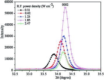 |
| | Fig. 2 X-ray diffraction 0002 peak of AZO thin films deposited by sputtering at RF power density of 0.31, 0.62, 1.23, 1.85, and 2.47 W cm−2. | |
Table 1 Bragg angles (2θ), full width at half maximum (β) and lattice parameter (c) of AZO thin films deposited by sputtering at different RF power densities
| RF power density (W cm−2) |
0.31 |
0.62 |
1.23 |
1.85 |
2.47 |
| 2θ (degree) |
33.85 |
34.10 |
34.21 |
34.24 |
34.18 |
| FWHM (degree) |
0.3609 |
0.3227 |
0.2983 |
0.2874 |
0.2865 |
| Lattice parameter, c ± 0.001, (Å) |
5.292 |
5.254 |
5.238 |
5.233 |
5.242 |
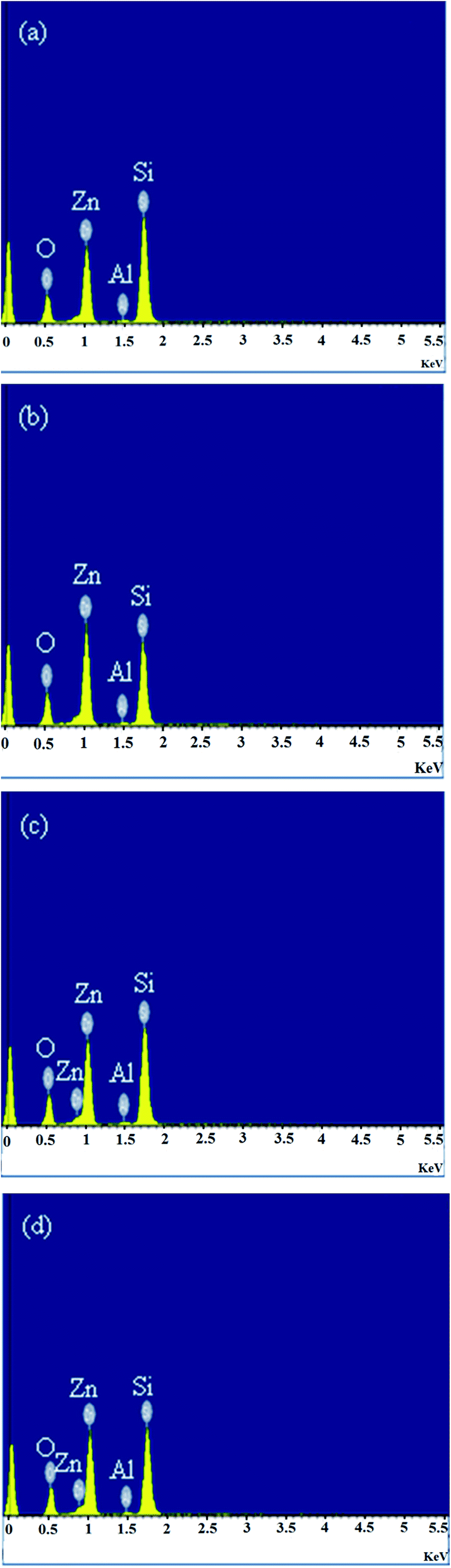
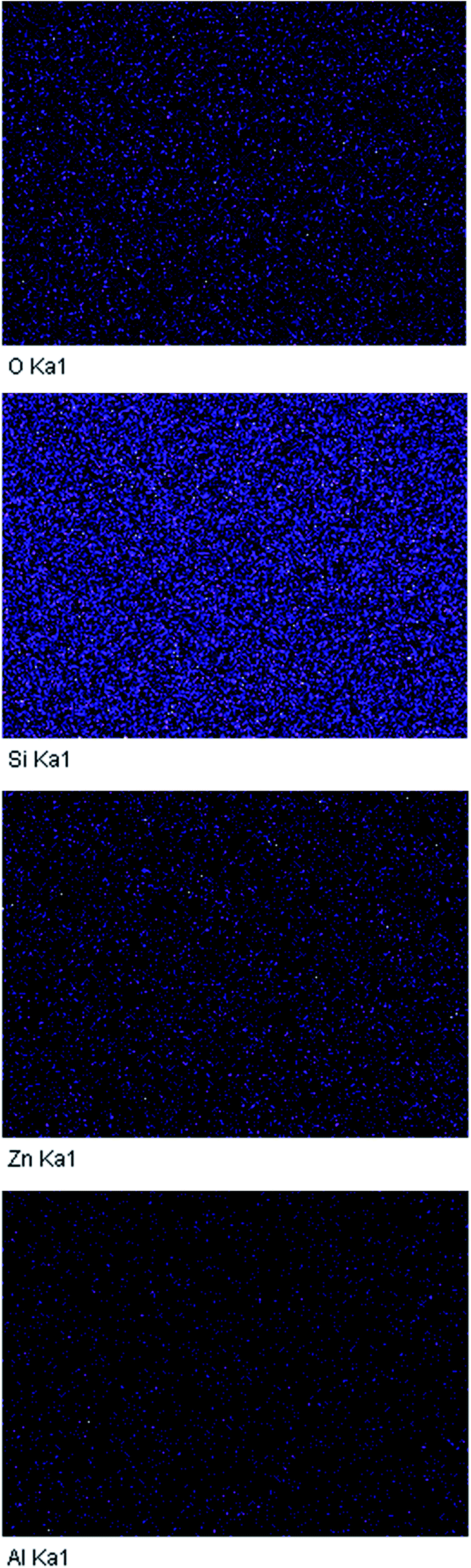
The chemical composition of the AZO thin films deposited at different RF power densities were analysed by energy dispersive system (EDS) using a spectrometer coupled to the scanning electron microscope (SEM). The spectrum reveals the presence of Zn, O and Al elements in the deposited films. The silicon signal appears from the substrate. The atomic percentages of elements in AZO films deposited at 0.62, 1.23, 1.85, and 2.47 W cm−2 are given in Table 2, Fig. 3(a–d). The atomic percentage of aluminum (Al) increases from 0.74 to 0.81 at% with increasing RF power density from 0.62 to 2.47 W cm−2. The elemental mapping (Fig. 4) of the film deposited at 0.62 W cm−2 was performed to look at Al distribution.
Table 2 Chemical composition of the AZO thin films deposited at different RF power densities
| RF power density (W cm−2) |
Atomic% |
| Al |
Zn |
O |
Si |
| 0.62 |
0.74 ± 0.03 |
18.90 ± 0.07 |
40.91 ± 0.23 |
39.45 ± 0.22 |
| 1.23 |
0.76 ± 0.03 |
23.09 ± 0.14 |
43.80 ± 0.16 |
32.35 ± 0.20 |
| 1.85 |
0.80 ± 0.04 |
20.43 ± 0.07 |
42.00 ± 0.19 |
36.77 ± 0.15 |
| 2.47 |
0.81 ± 0.03 |
21.77 ± 0.08 |
41.56 ± 0.31 |
35.86 ± 0.20 |
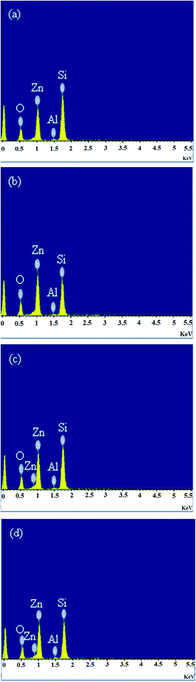 |
| | Fig. 3 Energy dispersive spectra of AZO thin films deposited by sputtering at RF power density of (a) 0.62, (b) 1.23, (c) 1.85, and (d) 2.47 W cm−2. | |
 |
| | Fig. 4 Elemental distribution maps of AZO thin films deposited by sputtering at RF power density of 0.62 W cm−2. | |
The microstructure of AZO thin films prepared at different RF power densities was examined by SEM (Fig. 5(a–d)).
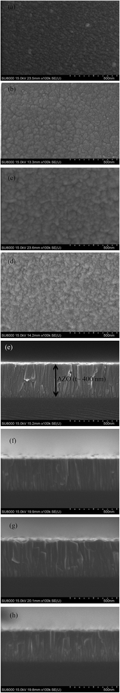 |
| | Fig. 5 SEM cross sectional images of AZO thin films (thickness ∼ 400 nm) deposited by sputtering at RF power density of (a, e) 0.62, (b, f) 1.23, (c, g) 1.85, and (d, h) 2.47 W cm−2, respectively. | |
Clearly, the microstructure of all samples showed uniform compact interconnected grains, free of flaws and cracks. By increasing the RF power density from 0.62 to 1.85 W cm−2, the grain size of the AZO thin films increased, which can be attributed to the improved mobility of the surface adatoms. Further increase of RF power density up to 2.47 W cm−2 leads to insignificant grain growth. This can be explained in terms of the growing-layer re-sputtering by the highly energetic impinging species.36 The cross-section SEM images (Fig. 5(e–h)) of AZO thin films (thickness, t ∼ 400 nm) prepared at different RF power densities exhibited a columnar structure with individual columnar grains extending upwards and perpendicular to the substrate. These observations are quite consistent with XRD and AFM analysis.
Three dimensional (3D) AFM images of AZO thin films are shown in Fig. 6. These have been analyzed by a scanning probe image processing (SPIP 6.0.14) software to obtain root-mean square roughness (Rrms) data. Accordingly, Rrms roughness increases up to a level and lies in the range 1.2–4.5 nm for the case of RF power density of 1.85 W cm−2, but decreases to 2.1 nm at 2.47 W cm−2, perhaps due to enhanced re-sputtering.36,37
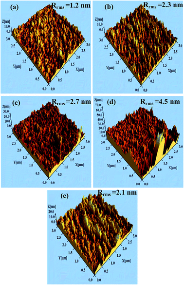 |
| | Fig. 6 Three dimensional AFM images of AZO thin films deposited by sputtering at RF power densities of (a) 0.31, (b) 0.62, (c) 1.23, (d) 1.85, and (e) 2.47 W cm−2. | |
3.2. Photoluminescence studies
Photoluminescence (PL) spectra of AZO thin films obtained with the excitation wavelength of 309 nm are shown in Fig. 7. Note that the AZO film deposited by sputtering at low RF power density of 0.31 W cm−2 exhibits emissions at 395 nm (near band edge), 405 and 422 nm (violet), 454 nm (blue), and 490 and 541 nm (green). The near band edge emission at ∼394 nm (3.15 eV) arises due to free exciton recombination and depends on the film crystallinity; the violet emission at 405 nm (3.06 eV) is attributed to the transition from the conduction band to the energy level of zinc vacancy (VZn).38,39 The violet emission at 422 nm is possibly related to transitions from interstitial zinc (Zni), or interface trap levels to the valance band.40,41 A strong blue emission peak at 454 nm (2.73 eV) is due to transitions from the shallow donor level of oxygen vacancy (VO), located at 0.3–0.5 eV below the conduction band, to the valance band.42 The green emissions at 490 nm (2.53 eV) and 541 nm (2.29 eV) correspond to Zni → VZn and the recombination of trapped electrons at the singly ionized oxygen vacancy ( ), with holes in the valence band, respectively.43–45 The charge transfer from neutral aluminum (Al0Zn) to zinc vacancies (VZn−) following the reaction Al0Zn + VZn− → AlZn+ + VZn2− gives rise to a green PL signal at 496 nm, but gets merged with the peak arising due to the Zni → VZn transition at around ∼490 nm.46 Fig. 8 shows a schematic diagram of energy levels with possible transitions responsible for various photoemissions. With increase of RF power density to 1.85 W cm−2, the resultant AZO films display improved photoluminescence corresponding to blue and green emissions at 2.73 and 2.53/2.29 eV, respectively. This suggests the emergence of increasing number of oxygen vacancies and zinc interstitials, possibly by irradiation effects. The release of electrons by oxygen vacancies should, however, increase the overall carrier density. Evidence for this fact is advanced via electrical and Hall measurements of AZO films (Section 3.3). The prominent changes in PL occurring below 454 nm can be related to the improved crystallinity of AZO films as mentioned above and revealed by X-ray diffraction as well (Section 3.1). The shift of the near band emission towards lower wavelength may be attributed to the increase of the energy band gap of AZO thin films following a rise in carrier concentration through aluminum ion (Al3+) insertion at Zn2+ sites and creation of additional oxygen vacancies.
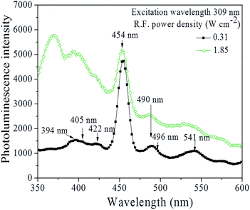 |
| | Fig. 7 Photoluminescence (PL) spectra of the RF sputtered AZO thin films at RF power densities of 0.31 and 1.85 W cm−2. | |
 |
| | Fig. 8 Schematic of energy levels with possible transitions. | |
3.3. Electrical and optical properties
The sheet resistance (R□) of AZO thin films deposited by sputtering at different RF power densities has been measured by four-point probe. The corresponding electrical resistivity data were deduced from ρ = R□ × t, where t is the film thickness. Hall measurements have been carried out to determine the nature of carriers and their concentrations (n). Once the electrical resistivity (ρ) and carrier concentration are known, mobility (μ) is obtained using the relation (1/ρ) = neμ, where e is the electronic charge. The experiments revealed n-type conductivity in AZO thin films. The electrical data collected are summarized in Table 3. Notice that the electrical resistivity decreases, while the carrier density increases progressively in AZO films, with the increase in RF power density employed for their deposition. However, the carrier mobility of AZO films decreases with the exception of the case of the RF power density of 1.85 W cm−2, where the value of μ is somewhat higher due to better crystallinity perhaps (Fig. 2). The enhanced electron and ionized impurity scattering of carriers appear to be dominant in reducing the mobility of AZO films.47 The AZO thin films deposited at RF power density of 2.47 W cm−2 yield a lower resistivity of 1.0 × 10⁻³ Ω cm. This resistivity value is better than the value (ρ ∼ 4.1 × 10⁻³ Ω cm) obtained in aluminum and gallium co-doped zinc oxide (GAZnO) thin film prepared by RF magnetron sputtering at room temperature, using 2 wt% aluminum and 1 wt% gallium as dopants in the ZnO,48 and comparable to the value (ρ ∼ 2.52 × 10⁻³ Ω cm) obtained by Wu et al.49 The high conductivity of the AZO thin films mainly results from non-stoichiometric composition and or aluminum doping. Electrons in these films are supplied from donor sites associated with oxygen vacancies or high valence metal ions (Al3+); therefore, the microstructure and doping have a strong influence on the electrical properties of the AZO films. The conductivity of AZO thin film is governed by the carrier concentration and mobility. The high carrier concentration is related to oxygen deficiency and Al3+ doping in ZnO. Each oxygen vacancy acts as an ionized donor and contributes one or two free electrons. Also, Al3+ substitutes for Zn2+ and creates a donor level near the conduction band. The grain growth may also release trapped electrons and raise the carrier concentration further. However, the carrier mobility is governed by scattering involving grain boundaries, phonons, electrons and ionized impurities.50 The grain boundary scattering is expected to be insignificant here as the electron mean free path (L ∼ 1 nm) is invariably much smaller than the crystallite size (D ∼ 23–29 nm) for the AZO films. Since the electron concentration of AZO thin films is significant and lies in the range of (n ∼ 1020 to 1021 cm−3), with grain size marginally different (D ∼23–29 nm), the electron–electron/impurities scattering mechanism seems to be largely limiting the mobility.51 The decrease in resistivity, despite of decrease in mobility, with increase in RF power density (Table 3) occurs because of disproportionate increase in the carrier concentration following the release of electrons via oxygen vacancies, Al3+ substitution on Zn site and the grain growth.
Table 3 Electrical and optical parameters of AZO thin films (thickness 400 nm) deposited by sputtering at different RF power densitiesa
| ΔEBM – Burstein–Moss shift, ΔEBGN – band gap narrowing, FTC – figure of merit. |
| RF power density (W cm−2) |
0.31 |
0.62 |
1.23 |
1.85 |
2.47 |
| Sheet resistance (R□) (Ω per square) |
140 |
77 |
53 |
27 |
25 |
| Resistivity (ρ) 10−3 (Ω cm) |
5.60 |
3.08 |
2.12 |
1.08 |
1 |
| Carrier concentration (n) 1020 (cm−3) |
0.60 |
1.44 |
3.34 |
3.98 |
6.26 |
| Mobility (μ) (cm2 V−1 s−1) |
18.60 |
14.09 |
8.83 |
14.54 |
9.98 |
| Optical energy band gap (Eg) (eV) |
3.41 |
3.51 |
3.57 |
3.59 |
3.62 |
| ΔEBM (meV) |
170 |
320 |
560 |
630 |
850 |
| ΔEBGN (meV) |
60 |
110 |
290 |
340 |
530 |
| FTC (103 Ω−1 cm−1) |
1.7 |
3.1 |
4.5 |
8.8 |
9.5 |
| Work function (Φ) (eV) |
3.90 |
3.92 |
4.40 |
4.42 |
4.44 |
The transmittance spectra of AZO thin films deposited by sputtering at different RF power densities are shown in Fig. 9. These exhibit an average transmittance of ∼90% in the visible region. Further, the absorption edge shifts towards a lower wavelength (or higher energy) in films produced with increasing RF power density. This possibly happens due to an increase in the carrier concentration. The optical energy band gap (Eg) of the film is deduced from the intercept of the linear fit of (αhν)2 vs. hν, or Tauc plot, with the energy axis (inset of Fig. 9), where α is the absorption coefficient (α = −lnT/t; T is transmittance, t is thickness of film). The resultant values of Eg increase from 3.41 to 3.62 eV with the increase in carrier concentration from 6 × 10¹⁹ to 6.26 × 1020 cm−3 (Table 3). A discussion on the variation in band gap with carrier density52–54 and improvement in the figure of merit (FTC)55 of AZO films with the increase in RF power density (Table 3) observed is given in the ESI (S1†).
 |
| | Fig. 9 Optical transmittance spectra of AZO thin films sputtered at various RF power densities; inset shows the corresponding (αhν)2 versus hν plots. | |
The Kelvin probe measures the average contact potential difference (Vcpd) between the tip and the sample, following the relation56
| −eVcpd = [φtip − φsample] |
where
φtip and
φsample represent the work functions of the Kelvin tip and the sample, respectively, and
e is the electronic charge. An apparent
Vcpd results due to charging of the tip and the sample with the existing ac voltage between them. This is nullified by an external bias (
Vdc) applied in the opposite direction. Under the condition,
Vcpd =
Vdc, the charges are eliminated altogether and the above expression yields
φsample if
φtip is known. Thus, with the application of both the ac voltage and external bias (
Vdc) between the tip and the sample, the work function can be deduced with the Kelvin probe when
Vdc becomes equal to
Vcpd. Thus, the work function of AZO films deposited by RF sputtering at power densities of 0.31, 0.62 1.23, 1.85, and 2.47 W cm
−2 were found to be 3.90, 3.92, 4.40, 4.42, and 4.44 ± 0.02 eV, respectively (
Table 3). The values improved further by 0.2–0.3 eV after subjecting the films to ozone treatment for 20 min. The above results suggest that the AZO films sputtered at RF power density of 2.47 W cm
−2 can serve as anodes (due to their high work function), whereas those produced at a low RF power density of 0.31 W cm
−2 are suitable for cathode application (work function being smaller) in OLEDs.
3.4. Bottom emitting organic light emitting diodes (BE-OLEDs)
Fig. 10 depicts the capacitance–voltage (C–V) characteristics of typical bottom emitting organic light emitting diodes fabricated with AZO thin films, deposited at low (0.62 W cm−2) as well as high (2.47 W cm−2) RF power densities, as anodes. For the sake of comparison, a reference device produced with a commercial ITO thin film has also been included in Fig. 10. Note that the device capacitance remains nearly the same or increases marginally up to a certain voltage (∼3.1–3.95 V), due to the accumulation of charge carriers,57 but decreases thereafter because of the recombination of carriers occurring in the organic layer progressively with the emission of light.58 Also, the turn-on voltage of the device decreases with the increase of the work function (Φ), the values being 3.95 and 3.50 V for Φ equal to 4.22 and 4.62 eV, respectively. The turn-on voltage of the AZO based device is somewhat higher than 3.1 V found in the commercial ITO based device, as the RF sputtered AZO thin films exhibit lower work function and higher resistivity; the work function (Φ) of commercial ITO film being 4.80 eV.
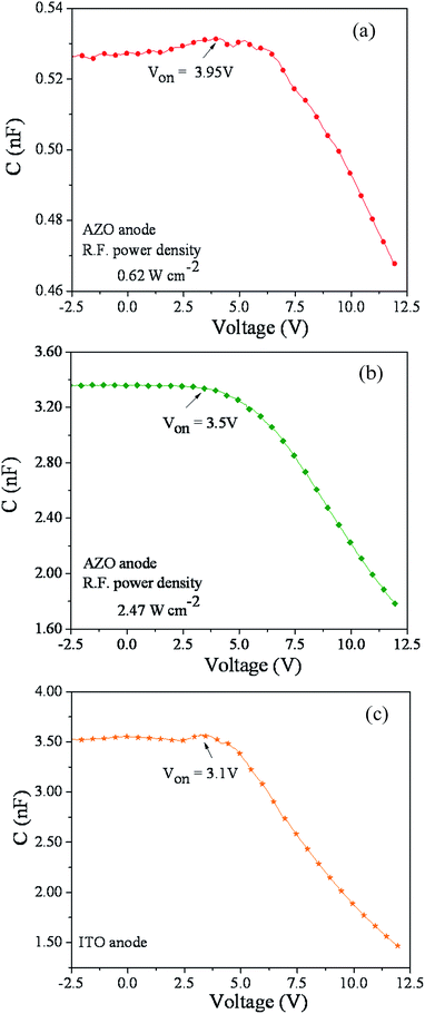 |
| | Fig. 10 Capacitance–voltage (C–V) characteristics of some typical bottom emitting OLEDs fabricated with (a, b) RF sputtered AZO at power density of 0.62 and 2.47 W cm−2, and (c) commercial ITO thin films as anode. | |
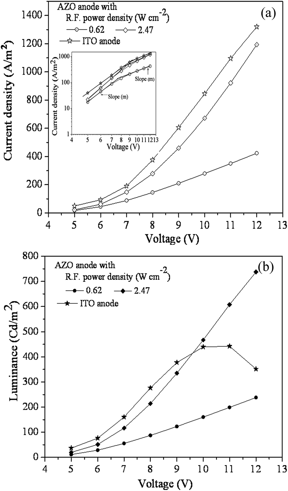
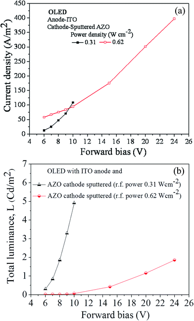
The current density–voltage–luminance (J–V–L) characteristics of various (AZO/ITO)/PEDOT:PSS/NPB/Alq3/BCP/LiF/Al devices are shown in Fig. 11. Their performance depends on charge injection, balance, and transport.59,60 Since the hole mobility is high in organic semiconductors, the injection barrier should be comparable or high, with respect to the cathode, to maintain charge balance and ensure recombination efficiency within the emissive layer.60,61 The variation in the device characteristics with the nature of the anode can be noticed in Fig. 11. In case of sputtered AZO films at low RF power density, the J–V curves shift towards a higher voltage. The luminance improves with applied voltage in all cases except ITO, where an increase occurs up to a certain voltage (e.g., ∼442 Cd m−2 at ∼11 V), but decreases thereafter. It may happen by charge imbalance, resulting in severe injection, due to a low barrier at the anode vis-a-vis the cathode.61,62 As a result, space charge is accumulated near the anode-organic layer interface at a higher bias and causes degradation. The performance of OLEDs is measured in terms of luminous flux power efficiency, given by η = πL/VJ = πγ/V, where L is the luminance, V is the applied voltage, J is the current density and γ (=L/J) is the luminance current efficiency.63 The values of η as deduced for bottom OLEDs, fabricated with AZO films (sputtered with RF power density of 2.47 W cm−2) and commercial ITO layers are 0.22 and 0.16 lm W−1, respectively at 10 V.
 |
| | Fig. 11 (a) Current density (J) versus voltage (V) with inset depicting the corresponding plot on a log–log scale; (b) luminance versus voltage (L–V) plot of bottom emitting OLEDs fabricated with RF sputtered AZO and commercial ITO thin films as the anode. | |
J–V characteristics (inset of Fig. 11(a)) of devices follow the power law, JαVm, with m assuming different values, depending on the bias ranges and the power density employed during the RF sputtering of AZO films. For example, at low voltages the values of m lie in the range 5–6, when the power density varies from 0.62 to 2.47 W cm−2. However, at higher voltages, it is just 2 for all the cases (inset of Fig. 11(a)). In contrast, the devices with ITO films correspond to m equal to 4 and 2 at low and high voltage regimes (inset of Fig. 11(a)). These characteristics are consistent with the space charge limited current observed in a trap-filled system.64–66
3.5. Transparent organic light emitting diodes
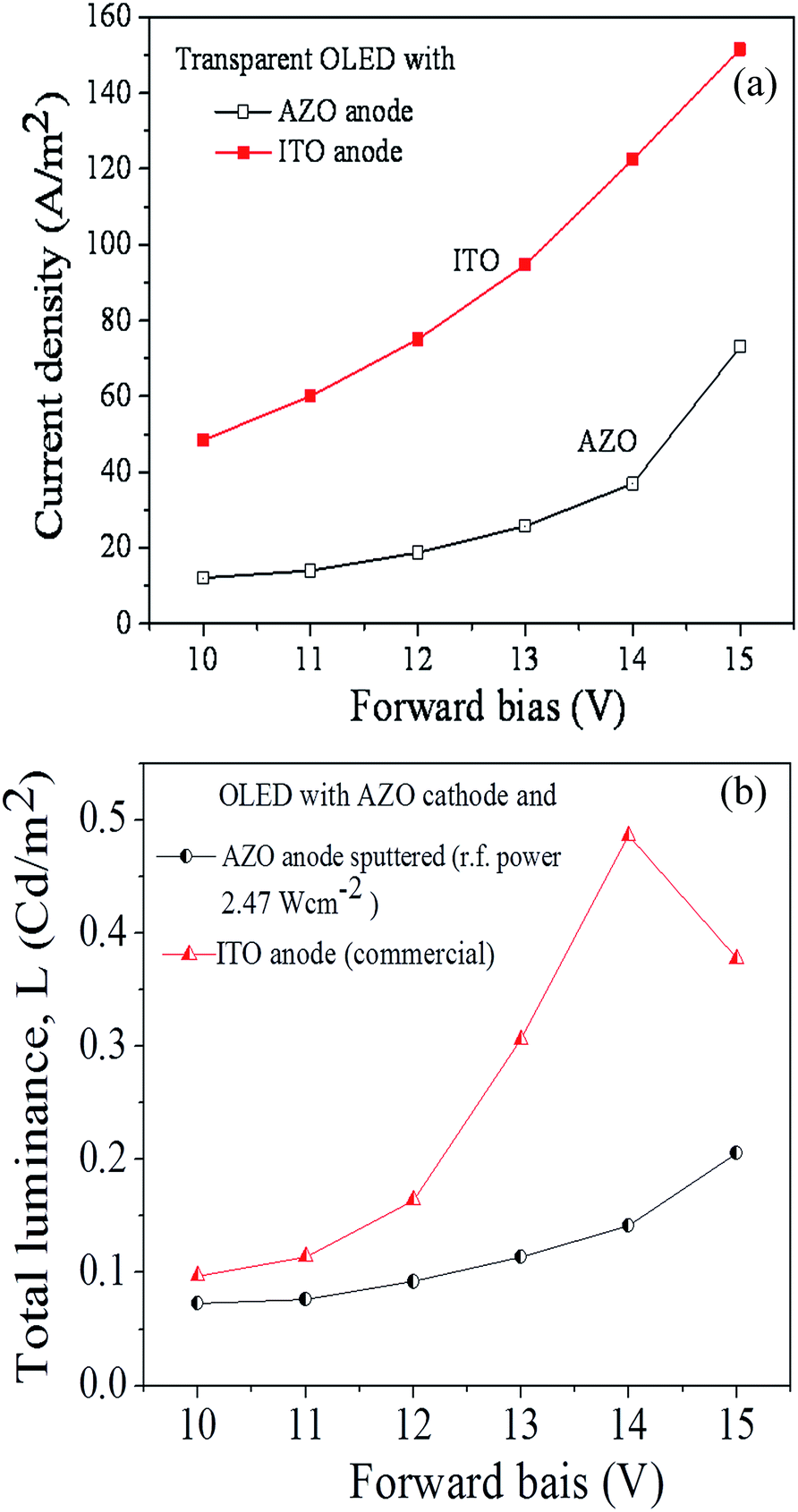
A cathode with low work function and good electron injection characteristics is vital for realizing a transparent organic light emitting diode.67 Although ITO is presently used as the cathode, it has a high work function, which makes it a poor electron injector.5,8,9 Hence, AZO films deposited by RF sputtering at the RF power density of 0.31 W cm−2 can possibly replace ITO as the cathode, due to their good electro-optical properties, coupled with low work function. On the other hand, AZO films formed at a higher power density of 2.47 W cm−2 display a high work function (like ITO) and so can serve as alternative anodes for OLEDs (Section 3.4). For comparative studies, ITO and AZO anode based transparent OLEDs have been fabricated with AZO thin films, prepared by sputtering at low RF power density of 0.31 W cm−2, as the cathode in both (Section 2). The OLED structure can be expressed as ITO (or AZO)/PEDOT:PSS/NPB/Alq3/BCP/LiF/AZO. The threshold voltage (Vth) for initiation of the recombination process was somewhat higher (∼10 V) in the case of a device having the AZO anode. With ITO as the anode, the device Vth was ∼9 V. Such a situation arises due to the difference in work function of ITO and AZO films, with values being 4.80 and 4.62 eV, respectively. The current density versus voltage and luminance versus voltage plots of transparent OLEDs fabricated with ITO and AZO thin films as anode are shown in Fig. 12(a) and (b), respectively. Their notable features are as follows:
 |
| | Fig. 12 (a) Current density versus voltage and (b) total luminance versus voltage plots of transparent OLEDs fabricated with ITO and AZO thin films (RF sputtered at power density of 2.47 W cm−2) as the anode; the cathode being AZO thin film sputtered at RF power density of 0.31 W cm−2. | |
(a) The current density is invariably lower in AZO based OLEDs and increases with increase in forward bias.
(b) ITO anode based OLEDs depict different trends in total luminance with the applied voltage, e.g., increase up to a certain voltage and then decrease in the former, and increase for the entire range of forward bias (10–15 V) in the latter case.
(c) Total luminance is higher in ITO-based OLEDs in comparison to AZO-based devices.
The lower current density of the AZO based transparent OLED can be attributed to (i) lower work function and (ii) high electrical resistivity of AZO films in comparison to ITO. The decrease in luminescence at the anode side in OLED with ITO above 14 V suggests degradation of the devices, possibly due to accumulation of holes near the anode and causes an increase in the electrical resistivity of the organic layer at a high current density. In contrast, the AZO based OLED remains stable. The reason seems to be the relatively low work function of AZO films and low current density displayed at high voltages. The reduction in charge carrier injection at the AZO/organic layer interface and, in turn, decrease in the forward current may occur at higher bias following degradation caused by radiation plasma during the deposition of AZO films via RF sputtering. Also, the sputtered species may penetrate into the organic layer and give rise to high leakage current. Note that the threshold voltage is much higher here than (4 V) found in bottom OLEDs (Section 3.4). It may be due to severe damage of the organic layer at the cathode side during the RF sputtering process, even though the work function of the AZO film is suitable (3.90 ± 0.02 eV) for efficient electron injection.
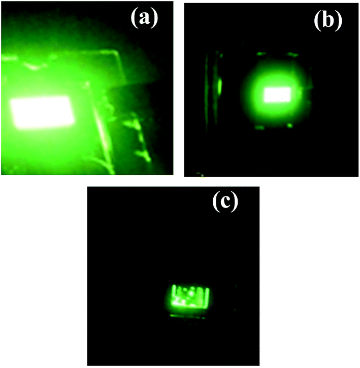
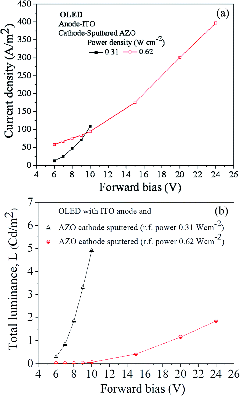
In both ITO and AZO based devices, the light extraction is less through the top electrode (cathode side), compared to the bottom electrode (ITO/AZO anode side) (Fig. 13). As mentioned earlier, this is due to the degradation of the AZO–organic layer interface. To protect the organic layer, a buffer multilayer of Alq3 (4.5 nm)/LiF (0.7 nm)/Al (15 nm) was laid over BCP by thermal evaporation (vacuum level ∼ 2 × 10⁻⁶ mbar). LiF not only improves the electron injection, but also, prevents the diffusion of aluminum species into the BCP layer. An additional Alq3 layer is used for further protection of the BCP. To demonstrate the degradation effect clearly, AZO film was deposited as the cathode by RF sputtering at power density of 0.31 and 0.62 W cm−2 in ITO anode based devices. The J–V characteristics of the resulting ITO/PEDOT:PSS/NPB/Alq3/BCP/Alq3/LiF/Al/AZO devices are shown in Fig. 14. Note that the device with the AZO cathode produced at higher power density shows higher leakage current density (J = 0.72 A m−2), presumably due to the massive damage of the organic layer caused even with the buffer layer in place. The leakage current is reduced by two orders of magnitude (∼4.7 × 10⁻³ A m−2) when RF power density is made half. Further, the threshold voltage (Vth) decreases from 10 V to 5 V, while the work function of the AZO film remains essentially the same at ∼3.92 ± 0.02 eV. The J–V–L characteristics of OLEDs are presented in Fig. 15. The total luminance is higher in devices having AZO films deposited by RF sputtering at lower power density. The comparison of devices further reveal that insertion of a buffer layer lowers the threshold voltage from 9 V to 5 V in the case of AZO film deposited by RF sputtering at the lowest power density of 0.31 W cm−2. The above results clearly indicate the effectiveness of the Alq3/LiF/Al buffer layer in protecting the organic layer during the deposition process of AZO films by RF sputtering.
 |
| | Fig. 13 Photographs of the transparent OLEDs with light emanating towards (a) ITO anode, (b) AZO anode and (c) AZO cathode. | |
 |
| | Fig. 14 Current density versus voltage (J–V) characteristics of transparent OLEDs fabricated with sputtered AZO films at RF power densities of 0.31 and 0.62 W cm−2 as the cathode, and ITO as the anode. | |
 |
| | Fig. 15 (a) Current density versus voltage plots of transparent OLEDs fabricated with ITO as anode and RF sputtered AZO thin films at power densities of 0.31 and 0.62 W cm−2 as cathode, (b) their total luminance emanating as a function of forward bias. | |
4. Conclusions
Transparent conducting AZO thin films deposited by RF sputtering at a power density of 2.47 W cm−2 and low substrate temperatures (75 °C) can be an alternative to ITO as the anode for bottom emitting OLEDs. The devices fabricated with AZO anode exhibit good charge balance, improved stability even at high current density, but a high turn-on voltage. The AZO films sputtered at a low power density (0.31 W cm−2) correspond to low work function, act as efficient electron injectors and so are suitable for the cathode of transparent OLEDs. The increase in RF power density during the sputtering of AZO films leads to perceptible damage of the organic layer, which, in turn, is responsible for raising the threshold and turn-on voltage of a transparent OLED. The introduction of a buffer layer of Alq3/LiF/Al just above the organic layer reduces the damage considerably, lowers the turn-on voltage, and improves the performance of transparent OLEDs.
Notes and references
- J. Lee, S. Hofmann, M. Furno, M. Thomschke, Y. H. Kim, B. Lüssem and K. Leo, Org. Electron., 2011, 12, 1383 CrossRef CAS.
- J. Huang, G. Li, E. Wu, Q. Xu and Y. Yang, Adv. Mater., 2006, 18, 114 CrossRef CAS.
- W. Brutting, S. Berleb and A. G. Muckl, Org. Electron., 2001, 2, 1 CrossRef CAS.
- C. C. Wu, C. I. Wu, J. C. Sturm and A. Kahn, Appl. Phys. Lett., 1997, 70, 1348 CrossRef CAS.
- G. Gu, V. Bulovic, P. E. Burrows, S. R. Forrest and M. E. Thompson, Appl. Phys. Lett., 1996, 68, 2606 CrossRef CAS.
- X. Zhou, M. Pfeiffer, J. S. Huang, J. B. Nimoth, D. S. Qin, A. Werner, J. Drechsel, B. Maennig and K. Leo, Appl. Phys. Lett., 2002, 81, 922 CrossRef CAS.
- J. T. Lim, C. H. Jeong, M. S. Kim, J. H. Lee, J. W. Bae and G. Y. Yeom, J. Korean Phys. Soc., 2007, 51, 1147 CrossRef CAS.
- G. Parthasarathy, P. E. Burrows, V. Khalfin, V. G. Kozlov and S. R. Forrest, Appl. Phys. Lett., 1998, 72, 2138 CrossRef CAS.
- G. Parthasarathy, C. Adachi, P. E. Burrows and S. R. Forrest, Appl. Phys. Lett., 2000, 76, 2128 CrossRef CAS.
- H. Kanno, Y. Sun and S. R. Forrest, Appl. Phys. Lett., 2005, 86, 263502 CrossRef.
- M.-H. Lu, M. S. Weaver, T. X. Zhou, M. Rothman, R. C. Kwong, M. Hack and J. J. Brown, Appl. Phys. Lett., 2002, 81, 3921 CrossRef CAS.
- J.-H. Lee, J. J. Huang, C.-C. Liao, P.-J. Hu and Y. Chang, Chem. Phys. Lett., 2005, 402, 335 CrossRef CAS.
- H. Chen, Y.-H. Jeong and C.-B. Park, Trans. Electr. Electron. Mater., 2009, 10, 58 CrossRef.
- H. Kim, A. Piqu, J. S. Horwitz, H. Murata, Z. H. Kafafi, C. M. Gilmore and D. B. Chrisey, Thin Solid Films, 2000, 377, 798 CrossRef.
- S. C. Gong, Y.-J. Choi, H. Kim, C.-S. Park, H.-H. Park, J. G. Jang, H. J. Chang and G. Y. Yeom, J. Vac. Sci. Technol., A, 2013, 31, 01A101 Search PubMed.
- I. Volintiru, M. Creatore, B. J. Kniknie, C. I. M. A. Spee and M. C. M. van de Sanden, J. Appl. Phys., 2007, 102, 043709 CrossRef.
- X. Jiang, F. L. Wong, M. K. Fung and S. T. Lee, Appl. Phys. Lett., 2003, 83, 1875 CrossRef CAS.
- D. Xu, Z. Deng, Y. Xu, J. Xiao, C. Liang, Z. Pei and C. Sun, Phys. Lett. A, 2005, 346, 148 CrossRef CAS.
- J. K. Jha, R. Santos-Ortiz, J. Du and N. D. Shepherd, J. Mater. Sci.: Mater. Electron., 2014, 25, 1492 CrossRef CAS.
- S.-H. Han, D.-B. Jo and K.-M. Le, Electron. Mater. Lett., 2013, 9(S), 43 CrossRef CAS.
- Z.-L. Tseng, P.-C. Kao, Y.-C. Chen, Y.-D. Juang, Y.-M. Kuo and S.-Y. Chu, J. Electrochem. Soc., 2011, 158, J310 CrossRef CAS.
- Q. You, H. Cai, K. Gao, Z. Hu, S. Guo, P. Liang, J. Sun, N. Xu and J. Wu, J. Alloys Compd., 2015, 626, 415 CrossRef CAS.
- C.-C. Chen and H.-C. Wu, Materials, 2016, 9, 164 CrossRef.
- R. Ebrahimifard, M. R. Golobostanfard and H. Abdizadeh, Appl. Surf. Sci., 2014, 290, 252 CrossRef CAS.
- W. Lee, S. Shin, D. R. Jung, J. Kim, C. Nahm, T. Moon and B. Park, Curr. Appl. Phys., 2012, 12, 628 CrossRef.
- J. H. Shin, D. K. Shin, H. Y. Lee, J. Y. Lee, N. I. Cho and S. J. Lee, J. Korean Phys. Soc., 2009, 55, 947 CrossRef CAS.
- J. Liu, W. J. Zhang, D. Y. Song, Q. Ma, L. Zhang, H. Zhang, X. B. Ma and H. Y. Song, Ceram. Int., 2014, 40, 12905 CrossRef CAS.
- Z. Y. Zhang, C. G. Bao, S. Q. Ma and S. Z. Hou, Appl. Surf. Sci., 2011, 257, 7893 CrossRef CAS.
- M. Bazzani, A. Neroni, A. Calzolari and A. Catellani, Appl. Phys. Lett., 2011, 98, 121907 CrossRef.
- M. H. Lee, Y. C. Peng and H. C. Wu, J. Alloys Compd., 2014, 616, 122 CrossRef CAS.
- Z.-L. Tseng, P.-C. Kao, C.-S. Yang, Y.-D. Juang and S.-Y. Chu, Appl. Surf. Sci., 2012, 261, 360 CrossRef CAS.
- G.-J. Zhou, W.-Y. Wong, B. Yao, Z. Xie and L. Wang, J. Mater. Chem., 2008, 18, 1799 RSC.
- N. Fujimura, T. Nishihara, S. Goto, J. Xu and T. Ito, J. Cryst. Growth, 1993, 130, 269 CrossRef CAS.
- M. K. Puchert, P. Y. Timbrell and R. N. Lamb, J. Vac. Sci. Technol., A, 1996, 14, 2220 CAS.
- Z. B. Fang, Z. J. Yana, Y. S. Tan, X. Q. Liua and Y. Y. Wang, Appl. Surf. Sci., 2005, 241, 303 CrossRef CAS.
- L. Monteagudo-Lerma, S. Valdueza-Felip, A. Núñez-Cascajeroa, M. González-Herráez, E. Monroy and F. B. Naranjo, Thin Solid Films, 2013, 545, 149 CrossRef CAS.
- H. Chou, P. I. Lin, C. C. Hsu, T. C. Chow, M. T. Hong, Y. C. Chen, J. R. Liu and T. P. Tsai, J. Vac. Sci. Technol., A, 2002, 20, 441 CAS.
- Y. H. Yang, H. G. Zhu and G. W. Yang, Appl. Phys. A, 2011, 103, 3 Search PubMed.
- B. Lin, Z. Fu and Y. Jia, Appl. Phys. Lett., 2001, 79, 943 CrossRef CAS.
- N. Boukos, C. Chandrinou, K. Giannakopoulos, G. Pistolis and A. Travlos, Appl. Phys. A, 2007, 88, 35 CrossRef CAS.
- X. Q. Wei, B. Y. Man, M. Liu, C. S. Xue, H. Z. Zhuang and C. Yang, Phys. B Condens. Matter, 2007, 388, 145 CrossRef CAS.
- Q. P. Wang, D. H. Zhang, H. L. Ma, X. H. Zhang and X. J. Zhang, Appl. Surf. Sci., 2003, 220, 12 CrossRef CAS.
- U. Ilyas, R. S. Rawat, T. L. Tan, P. Lee, R. Chen, H. D. Sun, L. Fengji and S. Zhang, J. Appl. Phys., 2011, 110, 093522 CrossRef.
- Y. Hu and H.-J. Chen, J. Nanopart. Res., 2008, 10, 401 CrossRef CAS.
- A. Ghosh and R. N. P. Choudhary, J. Phys. D: Appl. Phys., 2009, 42, 075416 CrossRef.
- Z.-Z. Li, M. Bao, S.-H. Chang, Z.-Z. Chen and X.-M. Ma, Vacuum, 2012, 86, 1448 CrossRef CAS.
- D. H. Zhang and H. L. Ma, Appl. Phys. A, 1996, 62, 487 CrossRef.
- B. Onwona-Agyeman, M. Nakao, T. Kohno, D. Liyanage, K. Murakami and T. Kitaoka, Chem.–Eng. J., 2013, 219, 273 CrossRef CAS.
- R. Wu, W. Zhang, H. Zhang, D. Song, Q. Ma, J. Liu, X. Ma, L. Zhang, L. Zhang and H. Song, Mater. Sci. Semicond. Process., 2014, 19, 24 CrossRef CAS.
- D. H. Zhang and H. L. Ma, Appl. Phys. A, 1996, 62, 487 CrossRef.
- K. L. Chopra, S. Major and D. K. Pandya, Thin Solid Films, 1983, 102, 1 CrossRef CAS.
- M. Caglar, S. Ilican, Y. Caglar and F. Yakuphanoglu, Appl. Surf. Sci., 2009, 255, 4491 CrossRef CAS.
- S.-M. Park, T. Ikegami, K. Ebihara and P.-K. Shin, Appl. Surf. Sci., 2006, 253, 1522 CrossRef CAS.
- J. Kumar and A. K. Srivastava, J. Appl. Phys., 2014, 115, 134904 CrossRef.
- R. E. I. Schropp and A. Madan, J. Appl. Phys., 1989, 66, 2027 CrossRef CAS.
- W. Melitz, J. Shena, A. C. Kummel and S. Lee, Surf. Sci. Rep., 2011, 66, 1 CrossRef CAS.
- B. G. Streetman and S. K. Banerjee, Solid state electronic devices, Pearson Education, Inc. and Dorling Kindersley (India) Pvt. Ltd., 2007 Search PubMed.
- L. Zhang, H. Nakanotani and C. Adachi, Appl. Phys. Lett., 2013, 103, 093301 CrossRef.
- C. Qiu, H. Chen and M. Wong, IEEE Trans. Electron Devices, 2001, 48, 2131 CrossRef CAS.
- A. Benor, S.-y Takizawa, C. P. Bolivar and P. Anzenbacher, Appl. Phys. Lett., 2010, 96, 243310 CrossRef.
- T. Mori, H. Fujikawa, S. Tokito and Y. Taga, Appl. Phys. Lett., 1998, 73, 2763 CrossRef CAS.
- P. Kumar, A. Misra, M. N. Kamalasanan, S. C. Jain and V. Kumar, J. Phys. D: Appl. Phys., 2007, 40, 561 CrossRef CAS.
- C. Qiu, H. Chen, M. Weng and H. S. Kwok, IEEE Trans. Electron Devices, 2001, 48, 2131–2137 CrossRef CAS.
- A. A. A. Ghamdia, O. A. A. Hartomya, B. M. Cavasc, F. E. Tantawyd and F. Yakuphanoglue, Optoelectron. Adv. Mater., Rapid Commun., 2012, 6, 292 Search PubMed.
- W. Chandra, L. K. Ang, K. L. Pey and C. M. Ng, Appl. Phys. Lett., 2007, 90, 153505 CrossRef.
- P. E. Burrows and S. R. Forrest, Appl. Phys. Lett., 1994, 64, 2285 CrossRef CAS.
- M. Pfeiffer, S. R. Forrest, X. Zhou and K. Leo, Org. Electron., 2003, 4, 21 CrossRef CAS.
Footnote |
| † Electronic supplementary information (ESI) available. See DOI: 10.1039/c6ra14124b |
|
| This journal is © The Royal Society of Chemistry 2016 |
Click here to see how this site uses Cookies. View our privacy policy here. 


 ), with holes in the valence band, respectively.43–45 The charge transfer from neutral aluminum (Al0Zn) to zinc vacancies (VZn−) following the reaction Al0Zn + VZn− → AlZn+ + VZn2− gives rise to a green PL signal at 496 nm, but gets merged with the peak arising due to the Zni → VZn transition at around ∼490 nm.46 Fig. 8 shows a schematic diagram of energy levels with possible transitions responsible for various photoemissions. With increase of RF power density to 1.85 W cm−2, the resultant AZO films display improved photoluminescence corresponding to blue and green emissions at 2.73 and 2.53/2.29 eV, respectively. This suggests the emergence of increasing number of oxygen vacancies and zinc interstitials, possibly by irradiation effects. The release of electrons by oxygen vacancies should, however, increase the overall carrier density. Evidence for this fact is advanced via electrical and Hall measurements of AZO films (Section 3.3). The prominent changes in PL occurring below 454 nm can be related to the improved crystallinity of AZO films as mentioned above and revealed by X-ray diffraction as well (Section 3.1). The shift of the near band emission towards lower wavelength may be attributed to the increase of the energy band gap of AZO thin films following a rise in carrier concentration through aluminum ion (Al3+) insertion at Zn2+ sites and creation of additional oxygen vacancies.