
 Open Access Article
 This Open Access Article is licensed under a
 Creative Commons Attribution 3.0 Unported Licence
Transformation of epitaxial NiMnGa/InGaAs nanomembranes grown on GaAs substrates into freestanding microtubes
C.
Müller
*a,
I.
Neckel
b,
M.
Monecke
c,
V.
Dzhagan
c,
G.
Salvan
c,
S.
Schulze
d,
S.
Baunack
e,
T.
Gemming
e,
S.
Oswald
e,
V.
Engemaier
e and
D. H.
Mosca
b
aTechnische Universität Chemnitz, Measurement and Sensor Technology, 09126 Chemnitz, Germany. E-mail: christian.mueller@etit.tu-chemnitz.de
bUniversidade Federal do Paraná, Departamento de Física, 81531-990 Curitiba, Brazil
cTechnische Universität Chemnitz, Solid Surfaces Analysis, 09126 Chemnitz, Germany
dTechnische Universität Chemnitz, Semiconductor Physics, 09126 Chemnitz, Germany
eIFW Dresden, Helmholtzstraße 20, 01069 Dresden, Germany
First published on 1st August 2016
Abstract
We report the fabrication of Ni2.7Mn0.9Ga0.4/InGaAs bilayers on GaAs (001)/InGaAs substrates by molecular beam epitaxy. To form freestanding microtubes the bilayers have been released from the substrate by strain engineering. Microtubes with up to three windings have been successfully realized by tailoring the size and strain of the bilayer. The structure and magnetic properties of both, the initial films and the rolled-up microtubes, are investigated by electron microscopy, X-ray techniques and magnetization measurements. A tetragonal lattice with c/a = 2.03 (film) and c/a = 2.01 (tube) is identified for the Ni2.7Mn0.9Ga0.4 alloy. Furthermore, a significant influence of the cylindrical geometry and strain relaxation induced by roll-up on the magnetic properties of the tube is found.
Introduction
Ferromagnetic shape memory alloys (FSMA) are a class of smart materials which are in scope for research due to their multifunctional properties. FSMA simultaneously exhibit ferromagnetism and ferroelasticity.1–4 The interactions among the ferromagnetic and ferroelastic order parameters, applied stress fields and applied magnetic fields are complex and may result in a variety of interesting phenomena. The most promising results to date have been achieved with the ferromagnetic Heusler alloy Ni2MnGa and in particular the family of Ni2+x+yMn1−xGa1−y. In these alloys magnetically controlled strains of up to 10% have been measured.5 The FSMA effect in these alloys is observed when the material undergoes the martensite transition. Depending on the chemical composition Ni–Mn–Ga alloys show a variety of martensitic structures with different magnetic properties.6–8 In particular, Ni–Mn–Ga thin films have received high attention due to their high potential as actuators and for micro-electro-mechanical systems (MEMS).9–14 Compared to the bulk material, thin films have better mechanical strength15,16 and show unique magnetic properties.17,18 Among various fabrication techniques like ion-beam sputtering,9 pulsed laser deposition,11 r.f.-sputtering12 and laser-beam ablation14 epitaxial growth has been considered as the most promising deposition technique to produce high quality films with high macroscopic strain. Deposition of epitaxial Ni–Mn–Ga films has been successfully realized on different substrates e.g. GaAs,19 MgO,20 SrTiO3,21 Al2O3,22 NaCl23,24 and YSZ.25 Frequently polycrystalline films were obtained, where the FSMA effect was suppressed due to grain boundaries. Recently, free-standing epitaxial Ni–Mn–Ga films with thickness in the micrometer-range have been fabricated and characterized. However, the structural and magnetic properties of Ni–Mn–Ga nanomembranes remain largely unexplored. Moreover, the control of composition and microstructure in thin films are challenging issues.In addition to epitaxial film growth, strain engineering offers an elegant approach to rearrange nanomembranes into three-dimensional micro- and nanotubes. Generally, the fabrication process requires a selective etching of the underlaying sacrificial layer to release the nanomembranes from their substrate and a certain amount of strain in the nanomembrane. Initially, molecular beam epitaxy (MBE) was used to fabricate strained bilayers based on semiconductors (i.e. InGaAs/GaAs26–28). More recently, first magnetic materials such as Fe3Si, have been introduced into epitaxial semiconductor/magnetic radial superlattices.29,30 In addition, other fabrication techniques were used to integrate magnetic materials into these rolled-up components.31–34 However, the integral magnetic properties of rolled-up Ni–Mn–Ga alloys and their potential for applications have not been studied yet. In this work, the fabrication of In0.2Ga0.8As/Ni–Mn–Ga nanomembranes on GaAs (001) substrate and their rolled-up freestanding counterparts is described in detail. We investigate the structural and magnetic properties with respect to the sample geometry.
Experimental
Initially, a strained bilayer consisting of 20 nm AlAs and 20 nm In0.2Ga0.8As was fabricated by III–V molecular beam epitaxy (MBE) on GaAs (001) substrates. After the first epitaxial growth the samples were transferred to a second custom designed ultra-high-vacuum MBE multichamber equipped with Ni, Mn, and Ga effusion cells. Prior to the growth of Ni–Mn–Ga, the MBE-grown III–V surface was thermally deoxidized at 423 K for 30 min. The removal of the oxide layer was controlled by RHEED analysis. The growth experiments were then performed at 423 K by opening the shutters during 40 min, resulting in a 40 nm thick Ni–Mn–Ga layer. To prepare the microtubes periodic stripes of 100 μm width, separated by 50 μm wide trenches were defined by photolithography along the (100) direction. A solution of H3PO4 (85%)–H2O2 (31%)–H2O (2![[thin space (1/6-em)]](https://www.rsc.org/images/entities/char_2009.gif) :10:500) was used to remove the Ni–Mn–Ga/InGaAs/AlAs layers of the trench. The high dilution of the etchants and the short etching time (<1 min) ensured the selective removal of the topmost layers. After lift-off the Ni–Mn–Ga/InGaAs/AlAs layer stack remained only at the 100 μm stripes. Tube formation was initiated by wet chemical removal of the AlAs sacrificial layer with 0.1% HF during 10 min. By releasing the strained bilayer from the substrate rolled-up InGaAs/Ni–Mn–Ga microtubes were prepared.
:10:500) was used to remove the Ni–Mn–Ga/InGaAs/AlAs layers of the trench. The high dilution of the etchants and the short etching time (<1 min) ensured the selective removal of the topmost layers. After lift-off the Ni–Mn–Ga/InGaAs/AlAs layer stack remained only at the 100 μm stripes. Tube formation was initiated by wet chemical removal of the AlAs sacrificial layer with 0.1% HF during 10 min. By releasing the strained bilayer from the substrate rolled-up InGaAs/Ni–Mn–Ga microtubes were prepared.
X-ray diffraction (XRD) θ/2θ measurements were performed in Brag–Brentano geometry using Cu-Kα radiation. Atomic force microscopy (AFM) images were obtained using a 5600LS microscope from Agilent. Ex situ X-ray photoemission spectroscopy (XPS) studies were performed with a PHI 5600 X-ray Photoelectron Spectrometer. The non-monochromatic Mg-Kα (hν = 1254.6 eV) X-ray source provides a spectral resolution of 1.1 eV for the Ag 3d5/2 peak. Quantification calculations were done using standard single element sensitivity factors.
Magnetic measurements on the planar samples and microtubes were carried out in a vibrating sample magnetometer (Quantum Design Evercool II) with field cooling (FC) and zero-field cooling (ZFC) magnetization measurements with magnetic field applied along the key directions to the sample. The morphology of the samples was studied by optical microscopy and scanning electron microscopy (SEM) using a FEI NanoSEM 200. To investigate the InGaAs/Ni–Mn–Ga microtube cross section a lamella was prepared by focused ion beam (FIB) cutting in a Zeiss NVision40. The TEM investigations have been done in a FEI Tecnai F30 operating at of 300 kV. The STEM mode was used for EDX analysis and imaging using the high angle annular dark field detector (HAADF). The planar sample was prepared by mechanical polishing and Ar-ion etching at 3 keV. The cross section of the film was analyzed with an energy-filtered Philips CM 20 FEG high resolution transmission electron microscope (HRTEM) equipped with Gatan GIF operated at 200 kV.
Results and discussion
Surface morphology
The surface of the as prepared epitaxial nanomembranes was analysed by AFM. The topography measurements show a nanocrystalline texture (Fig. 1(a)) and a typical root mean square roughness (RMS) of ∼1 nm. After definition of the stripes by photolithography and selective etching of the trench cross-section analysis was performed by AFM. From the profile taken along the indicated direction in Fig. 1(b) a total height for the Ni–Mn–Ga/InGaAs/AlAs layer stack of 80 nm was obtained, resulting in an effective layer thickness for Ni–Mn–Ga of 40 nm.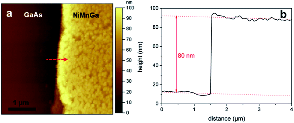 | ||
| Fig. 1 (a) Atomic force microscopy topography image taken near the boundary of a Ni–Mn–Ga/InGaAs/AlAs stripe and GaAs. (b) Corresponding cross-sectional analysis of the height, with the measurement direction as indicated in (a). | ||
XPS analysis
Fig. 2 shows the Ni 2p3/2, Mn 2p3/2 and Ga 2p3/2 peaks of the film obtained from XPS after sputtering with Ar ions for 2 min (removed ∼7 nm of the topmost layer).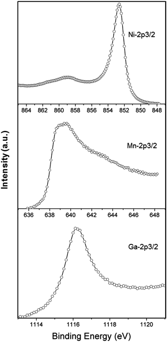 | ||
| Fig. 2 Ni 2p3/2, Mn 2p3/2 and Ga 2p3/2 XPS peaks of Ni2.7Mn0.9Ga0.4 after surface cleaning with Ar-ions. | ||
The peaks appear at 852 eV, 639 eV and 1116 eV, respectively. The short Ar ion sputtering step removed surface contaminations, e.g. native oxide, and carbon species, and increased significantly the intensity of the Ni 2p3/2, Mn 2p3/2 and Ga 2p3/2 peaks, enabling to determine the composition of the alloy to Ni2.7Mn0.9Ga0.4. It is known from earlier works35 that the composition is strongly related to the sputtering time. To prove the composition, EDX-analysis was performed inside a SEM (not shown). From the measurements similar composition were obtained for the Ni–Mn–Ga alloy with deviations of <4 at% from the XPS data.
XRD and TEM analysis
The crystallographic structures of the substrate and the constrained Ni–Mn–Ga film have been analyzed by XRD with θ–2θ scans. The intensity of the GaAs (004) Bragg peak was used to normalize the XRD patterns. In Fig. 3 there are two peaks from the Ni–Mn–Ga film, which can be assigned to the (103) and (114) Bragg reflections, indicating a tetragonal structure with c/a > 1.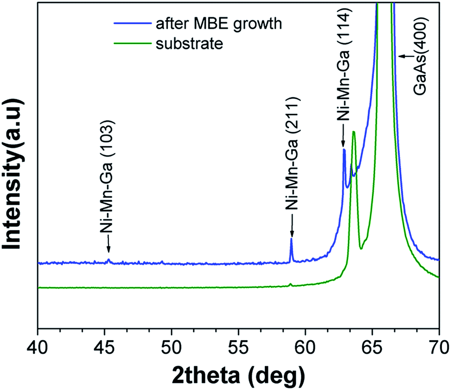 | ||
| Fig. 3 XRD pattern of Ni2.7Mn0.9Ga0.4 films and GaAs substrate measured at room temperature. | ||
To examine the crystal structure more in detail TEM experiments were performed on the films. Fig. 4(a) shows the cross section of the film. The GaAs, AlAs, InGaAs and Ni–Mn–Ga layers can be clearly identified by their different mass-thickness contrast. However, the interface between Ni–Mn–Ga and InGaAs is not clearly visible, allowing only an estimation of the layer thickness. The diffraction pattern taken from the Ni–Mn–Ga layer shows a combination of diffuse rings and spots, indicating a polycrystalline nature (Fig. 4(b)). After analyzing the position of the (112) and (200) diffraction rings a body centered tetragonal, L10 structure (I4/mmm) with lattice parameter a = b = 3.58 Å, c = 7.27 Å, and c/a = 2.03 was found. This result is comparable with diffraction data for Ni2Mn1.2Ga0.8 of ref. 36, reporting a = b = 3.7 Å, c = 7.1 Å. Shao Meng et al.37 found a = b = 3.9 Å, c = 6.4 Å for Ni2.1Mn0.9Ga. However, in the present work an alloy with significant higher amount of Ni was obtained.
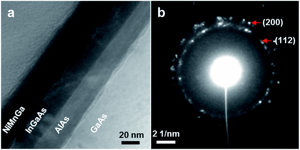 | ||
| Fig. 4 (a) HRTEM cross section of the Ni–Mn–Ga/InGaAs/AlAs/GaAs layer stack. (b) Corresponding selected area electron diffraction (SAED) of the Ni–Mn–Ga layer with electron beam orientated along the in-plane. | ||
After releasing the strained InGaAs/Ni–Mn–Ga bilayers from the substrate rolled-up double microtubes orientated along the GaAs (100) axis with a typical radius of 2.5 μm, measured by scanning electron microscopy (SEM), and a length of several millimeters were obtained (Fig. 5(a) and (b)).
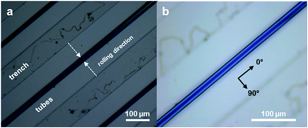 | ||
| Fig. 5 Optical microscopy images: (a) taken from the tube array. The rolling direction is indicated with bright arrows. (b) Showing two rolled-up double tubes with ∼5 μm diameter. | ||
Fig. 6 summarizes the results from cross-sectional microscopic analysis. According to the tube radius and the stripe size microtubes with three periods are obtained (Fig. 6(a) and (b)). Defined FIB thinning of tubular structures was adversely affected by the cavity and loose rolling. During lamella preparation only one of the twin tubes shown in Fig. 5(b) survived. The lower layer in Fig. 6(b) is material redeposited during FIB milling (mainly GaAs). The layer thickness of InGaAs and for the Ni–Mn–Ga layer was measured to 20 nm and 40 nm, respectively, in agreement with the nominal deposition parameters and the AFM investigations. The Ni–Mn–Ga layer appears polycrystalline with grain sizes of about 20 nm. An EDX line scan was were carried out over the marked line of the layer stack (Fig. 7(a)). The element intensities allow to clearly distinguish between the three different materials NiMnGa, InGaAs, and GaAs redeposited during FIB cutting (Fig. 7(b)). The compositional analysis of the NiMnGa layer of the tube gave Ni2.7MnGa0.3 which is close to the XPS data. The oxygen signal is higher in the NiMnGa layer than in the GaAs without remarkable enrichment at the interfaces. This probably originates from oxygen incorporated during deposition. Similar results were observed in other rolled-up structures.29
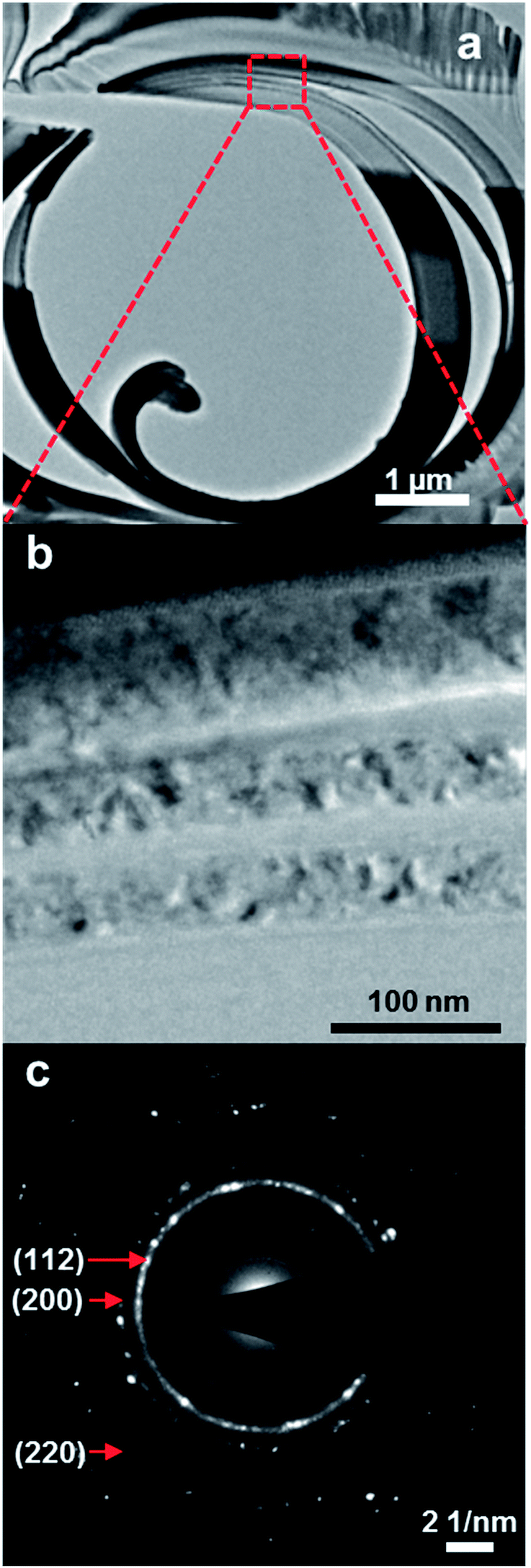 | ||
| Fig. 6 (a) SEM cross section of the rolled-up Ni–Mn–Ga/InGaAs bilayer. (b) Corresponding HRTEM image of the marked area in (a). (c) Corresponding selected area electron diffraction (SAED) of the rolled-up Ni–Mn–Ga layer. | ||
 | ||
| Fig. 7 (a) EDX line scan and HAADF brightness inside the rolled up structure. (b) HAADF-STEM image with location of the EDX line scan. The image is located near the right edge of the marked area in Fig. 6(a). The line scan spans from a partly thinned NiMnGa layer (upper) to GaAs redeposited in the hollow tube interior. | ||
The crystal structure of the rolled-up Ni–Mn–Ga was investigated by HRTEM (Fig. 6(c)). The diffraction pattern shows a combination of rings and spots, indicating a polycrystalline layer. Based on the diffractions rings the crystalline structure can be indexed as body centered tetragonal, L10 structure (I4/mmm; a = b = 3.51 Å, c = 7.06 Å, c/a = 2.01).
That means after roll-up the same lattice type as for the film is observed. When comparing the results from the microtube with the film, a slight mismatch between the lattice parameters of 2%, 3% and 1%, respectively for a, c and c/a can be found. The difference can be seen as an indication for tensile strain in the NiMnGa film. During roll-up of the strained bilayer relaxation can take place, accompanied by a decrease of the lattice parameters of NiMnGa. At the same time the compressed InGaAs layer (a = 5.85 Å for the film) is released.
Magnetic properties
Magnetization measurements were carried out on the strained InGaAs/Ni–Mn–Ga bilayer and the corresponding rolled-up tubes along the main directions. The hysteresis curves measured at 10 K for the magnetic field applied along the two [010] directions (0° and 90° to the tube axis, in-plane) and [001] direction (out-of-plane) are shown in Fig. 8. Typical ferromagnetic behavior and strong magnetic in-plane anisotropy is observed for the film Fig. 8(a). | ||
| Fig. 8 Magnetization curves measured at 10 K with the magnetic field applied along the two [010] directions (0° and 90° to the stripe/tube axis, in-plane) and [001] direction (out-of-plane): (a) of Ni2.7Mn0.9Ga0.4 films and (b) after roll-up. (c) Magnetization curves for film and tube measured at 300 K. | ||
Saturation magnetizations Ms of 560 emu cm−3 at 4 T were obtained when taking into account the film dimensions. Measurements along both in-plane directions exhibit atypical easy axis rectangular loop with a coercivity (Hc) of ∼25 mT. The coercivity along [001] is significant larger (100 mT) and the hysteresis curve is more tilted.
After roll-up the in-plane magnetization curves exhibit a smoother shape, indicating harder switching behavior (Fig. 8(b)).
Furthermore, the hysteresis curve of the in-plane direction (0°, tube long axis) coincides with the out-of-plane direction (tube short axis). The coercivity along [001] is significant larger (∼130 mT) and the hysteresis curve is more tilted. These results indicate that shape anisotropy of the tube plays a minor role. The polycrystalline character of the NiMnGa layer and the absence of a pronounced microstructure allow us to attribute this change of anisotropy due to magnetoelastic effect (stress). Then the change of stress induced by roll-up along the 90° direction can be estimated from the intersection of both hysteresis curves measured along 90°. This gives an average anisotropy field of HA = 2K/Ms of 65 mT, which is related to an anisotropy constant of K = 18.4 kJ m−3. The difference of stress can be calculated from K = 3/2λsσ, where λs is the magnetostrictive constant and σ is the stress. Using a value for NiMnGa of λs = 1.3 × 10⁻⁴ (ref. 38) one obtains a difference of stress between film and rolled-up tube of 94 MPa, indicating a higher tensile stress along the 90° axis of the film. The orientation of the easy axis of the film seems to be supported by this stress, originating from the lattice mismatch between GaAs and InGaAs/Ni–Mn–Ga bilayer. After roll-up stress release occurs preferentially along the 90° axis (rolling axis) and therefore tilting of the hysteresis curve is observed. As expected from geometry all perpendicular directions to the long tube axis behave similar. Similar observations after roll-up were made in.29 Roll-up of the strained bilayer induces compression of NiMnGa along the 90° axis. Probably, a tensile strength remains along the 0° direction due to incomplete underetching between neighbouring tubes, resulting in similar magnetization curves as observed in Fig. 8(b). Strain relaxation also can be seen as the reason for strong increase of coercivity along the 0° and 90° axis. Important to note, that the result from stress evolution found by magnetization measurements is in agreement with our data from TEM, showing a small drop of the lattice parameters after roll-up.
In addition, the temperature dependence of the ZFC and FC magnetizations is shown in Fig. 9 measured in the range 10 ≤ T ≤ 400 K under a magnetic field of 50 mT. Film (Fig. 9(a)) and tubes (Fig. 9(b)) show similar results. The ZFC magnetization initially increases with decreasing temperature and passes a maximum at Tmax = 150 K, indicating a transition from superparamagnetic to ferromagnetic behavior. Above Tmax the samples become magnetically isotropic, which is also observed in the in-plane hysteresis loops measured at 300 K (Fig. 8(c)). Whereas below Tmax a splitting of the FC and ZFC curves is observed, implying the presence of magnetically blocked states. The ZFC-FC irreversibility found in this work is consistent with reports on polycrystalline Ni50Mn35Ga15 samples with tetragonal structure.39,40 Similar to aforementioned mentioned works no martensitic transformations can be seen in the magnetization curves due to the nanocrystalline nature.
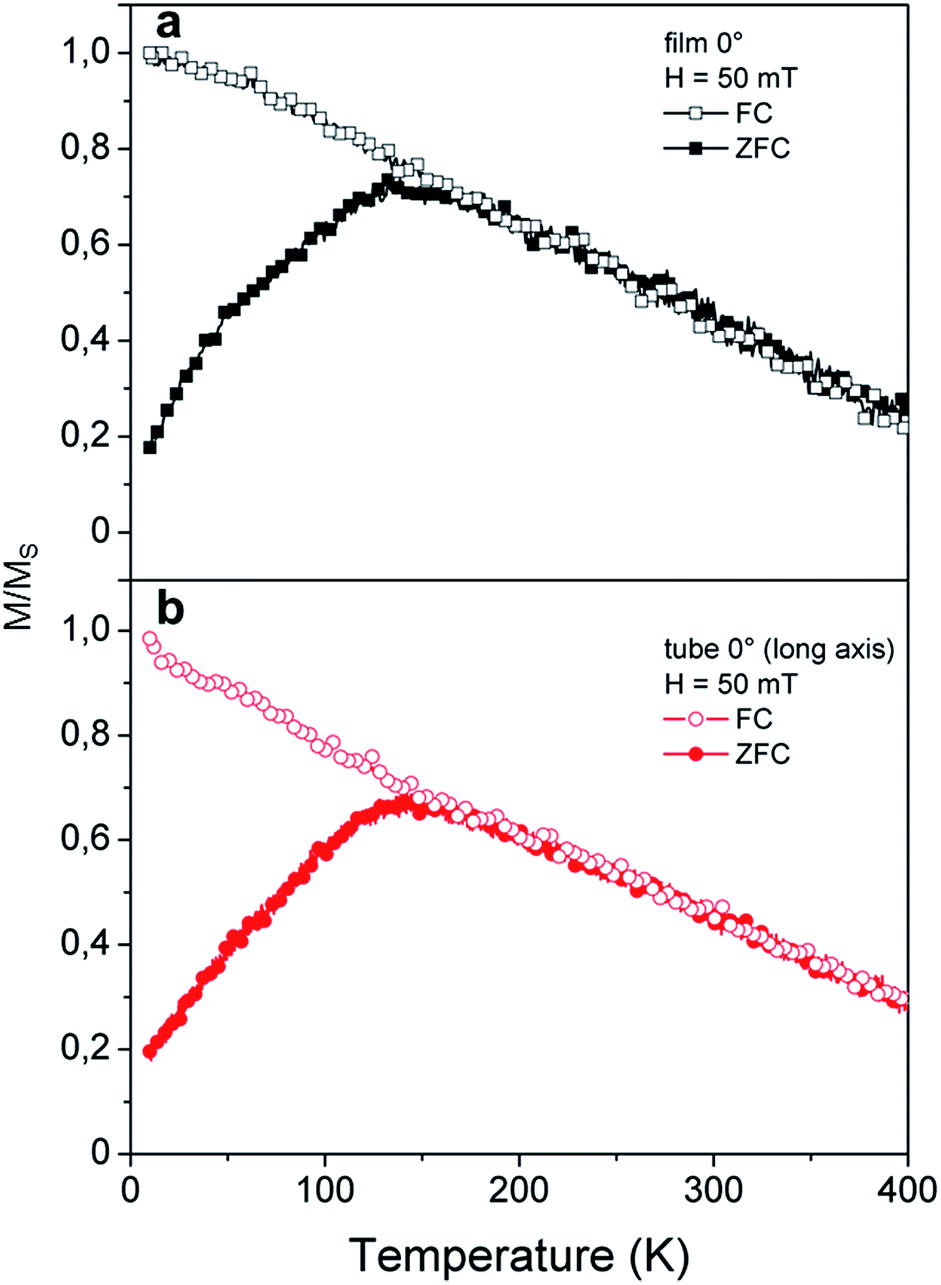 | ||
| Fig. 9 ZFC and FC magnetization curves for a cooling field of 50 mT with the magnetic field applied along the 0° direction: (a) of Ni53Mn28Ga19 films and (b) after roll-up. | ||
Conclusions
In conclusion, we have shown a fabrication route to realize freestanding FSMA based on Ni–Mn–Ga alloys grown by molecular beam epitaxy on GaAs. The evolution of structural and magnetic properties induced by roll-up is investigated in detail. Our results prove the influence of crystallographic orientation and strain state on structural and magnetic properties of Ni–Mn–Ga nanomembranes and their tubular counterparts. These insights are fundamental in order to realize thin nanomembranes and freestanding three-dimensional FSMA structures with composition of choice for smart applications as compact actuators and microsensors.Acknowledgements
The work was financially supported by CNPq, SISNANO and Coordenação de Aperfeiçoamento de Pessoal de Nível Superior (CAPES), Brazil, no. A083/2013. We thank Prof. M. Hietschold and D. Dentel for access to the TEM facilities. Prof. D. R. T. Zahn is thanked for support.Notes and references
- K. Ullakko, J. K. Huang, C. Kantner, R. C. O'Handley and T. A. Lograsso, Appl. Phys. Lett., 1996, 69, 1966 CrossRef CAS.
- O. Heczko, J. Magn. Magn. Mater., 2005, 290/291, 787 CrossRef.
- N. Sarawate and M. Dapino, Appl. Phys. Lett., 2006, 88, 121923 CrossRef.
- J. Tellinen, I. Suorsa, A. Jaaskelainen, I. Aaltio and K. Ullakko, Scr. Mater., 2003, 49, 566 Search PubMed.
- P. Mullner, V. A. Chernenko and G. Kostorz, Mater. Sci. Eng., A, 2004, 387–389, 566 Search PubMed.
- V. A. Chernenko, V. V. Kokorin and I. N. Vitenko, Scr. Metall. Mater., 1995, 33, 1239 CrossRef CAS.
- R. W. Overholsen, M. Wuttig and D. A. Neumann, Scr. Mater., 1999, 40, 1095 CrossRef.
- J. Pons, V. A. Chernenko, R. Santamarta and E. Cesari, Acta Mater., 2000, 48, 3027 CrossRef CAS.
- J. P. Ahn, N. Cheng, T. Lograsso and K. M. Krishnan, IEEE Trans. Magn., 2001, 37, 2141 CrossRef CAS.
- J. W. Dong, L. C. Chen, J. Q. Xie, T. A. Müller, D. M. Carr, C. J. Palmstrom, S. McKernan, Q. Pan and R. D. James, J. Appl. Phys., 2000, 88, 7357 CrossRef CAS.
- P. G. Tello, F. J. Castano, R. C. O'Handley, S. M. Allen, M. Esteve, A. Labarta and X. Batlle, J. Appl. Phys., 2002, 91, 8234 CrossRef CAS.
- S. K. Wu, K. H. Tseng and J. Y. Wang, Thin Solid Films, 2002, 408, 316 CrossRef CAS.
- M. Kohl, S. Hoffmann, Y. Liu, M. Ohtsuka and T. Takagi, J. Phys. IV, 2003, 112, 1185 CAS.
- C. Y. Chung, V. A. Chernenko, V. V. Khovailo, J. Pons, E. Cesari and T. Takagi, Mater. Sci. Eng., A, 2003, 378, 443 CrossRef.
- M. Suzuki, M. Ohtsuka, T. Suzuki, M. Matsumoto and H. Miki, Mater. Trans. JIM, 1999, 40, 1174 CrossRef CAS.
- M. Ohtsuka and K. Itagaki, International Journal of Applied Electromagnetics and Mechanics, 2000, 12, 49 Search PubMed.
- T. J. Zhu, L. Lu, M. O. Lai and J. Ding, Smart Mater. Struct., 2005, 14, S293 CrossRef CAS.
- V. O. Golub, A. Y. Vovk, L. Malkinski, C. J. O'Connor, Z. Wang and J. Tang, J. Appl. Phys., 2004, 96, 3865 CrossRef CAS.
- J. W. Dong, L. C. Chen, C. J. Palmstrom, R. D. James and S. McKernan, Appl. Phys. Lett., 2004, 75, 1443 CrossRef.
- O. Heczko, M. Thomas, J. Buschbeck, L. Schultz and S. Fähler, Appl. Phys. Lett., 2008, 92, 072502 CrossRef.
- A. Backen, S. R. Yeduru, M. Kohl, S. Baunack, A. Diestel, B. Holzapfel, L. Schultz and S. Fähler, Acta Mater., 2010, 58, 3415 CrossRef CAS.
- G. Jakob, T. Eichhorn, M. Kallmayer and H. Elmers, Phys. Rev. B: Condens. Matter Mater. Phys., 2007, 76, 174407 CrossRef.
- O. Heczko, M. Thomas, R. Niemann, L. Schultz and S. Fähler, Appl. Phys. Lett., 2009, 94, 152513 CrossRef.
- M. Thomas, O. Heczko, J. Buschbeck, Y. W. Lai, J. McCord, S. Kaufmann, L. Schultz and S. Fähler, Adv. Mater., 2009, 21, 3708 CrossRef CAS.
- Y. P. Zhang, R. A. Hughes, J. F. Britten, J. S. Preston, G. A. Botton and M. Niewczas, Phys. Rev. B: Condens. Matter Mater. Phys., 2010, 82, 054406 CrossRef.
- V. Y. Prinz, V. A. Selezenev, A. K. Gutakovsky, A. V. Chehovskiy, V. V. Preobrazhenskii, M. A. Putyato and T. A. Gavrilova, Phys. E, 2000, 6, 828 CrossRef CAS.
- O. G. Schmidt and K. Eberl, Nature, 2001, 410, 168 CrossRef CAS PubMed.
- C. Deneke, U. Zschieschang, H. Klauk and O. G. Schmidt, Appl. Phys. Lett., 2006, 89, 263110 CrossRef.
- C. Deneke, J. Schuhmann, R. Engelhard, J. Thomas, C. Müller, M. S. Khatri, A. Malachias, M. Weisser, T. H. Metzger and O. G. Schmidt, Nanotechnology, 2009, 20, 045703 CrossRef PubMed.
- F. Balhorn, S. Mansfeld, A. Krohn, J. Topp, W. Hansen, D. Heitmann and S. Mendach, Phys. Rev. Lett., 2010, 104, 037205 CrossRef PubMed.
- I. Mönch, D. Makarov, R. Koseva, L. Baraban, D. Karnaushenko, C. Kaiser, K. F. Arndt and O. G. Schmidt, ACS Nano, 2011, 5, 7436 CrossRef PubMed.
- C. Müller, C. C. Bof Bufon, M. E. Navarro Fuentes, D. Makarov, D. H. Mosca and O. G. Schmidt, Appl. Phys. Lett., 2012, 100, 022409 CrossRef.
- D. Karnaushenko, D. D. Karnaushenko, D. Makarov, S. Baunack, R. Schäfer and O. G. Schmidt, Adv. Mater., 2015, 27, 6582 CrossRef CAS PubMed.
- R. Streubel, L. Han, F. Kronast, A. A. Ünal, O. G. Schmidt and D. Makarov, Nano Lett., 2014, 14, 3981 CrossRef CAS PubMed.
- C. Biswas and S. R. Barman, Appl. Surf. Sci., 2006, 252, 3380 CrossRef CAS.
- N. Jetta, Master thesis, Osmania University, 2010.
- Y. Shao Meng, P. Jian, C. Bo and L. Jian, Chin. Sci. Bull., 2011, 56, 796 CrossRef.
- V. A. L'vov, Ukr. J. Phys., 2005, 50, 763 Search PubMed.
- Z. D. Han, B. Qian, D. H. Wang, P. Zhang, X. F. Jiang, C. L. Zhang and Y. W. Du, Appl. Phys. Lett., 2013, 103, 172403 CrossRef.
- I. T. Neckel, W. H. Schreiner and D. H. Mosca, Intermetallics, 2015, 67, 127 CrossRef CAS.
| This journal is © The Royal Society of Chemistry 2016 |