
Non-interacting, sp2 carbon on a ferroelectric lead zirco-titanate: towards graphene synthesis on ferroelectrics in ultrahigh vacuum†
N. G. Apostola,
G. A. Lungua,
I. C. Bucurab,
C. A. Tachec,
L. Hriba,
L. Pintiliea,
D. Macoveia and
C. M. Teodorescu*a
aNational Institute of Materials Physics, Atomiştilor 105b, 077125 Măgurele, Ilfov, Romania. E-mail: teodorescu@infim.ro
bUniversity of Bucharest, Faculty of Physics, Atomiştilor 405, 077125 Măgurele, Ilfov, Romania
cUniversity of Trieste, Department of Physics, Via Valerio 2, 34127 Trieste, Italy
First published on 12th July 2016
Abstract
Carbon layers grown on lead zirco-titanate (PZT) weakly interact with the substrate and exhibit a nearly two dimensional character, up to a carbon surface density approaching that of graphene. The first feature is evidenced by X-ray photoelectron spectroscopy, and the second by angle resolved near-edge-absorption spectroscopy (NEXAFS). The binding energies and lineshape parameters of C 1s are similar to that of graphene. The dichroism of C K-edge NEXAFS shows the prevalence of in-plane sp2 bonds for layers whose effective coverage is below the graphene surface density. The polarization state of the substrate, oriented outwards, is preserved upon carbon deposition. The surface Pb content is strongly affected by the carbon ad-layers.
Intensely studied applications nowadays are related to the fact that graphene may be regarded as a perfect semimetal with large carrier mobility, making structures involving graphene conduction channel suitable candidates for ultrahigh frequency field effect transistors.1 Graphene bilayers under an applied perpendicular electric field exhibit an exploitable gap in logic applications.2 Growth or transfer of graphene monolayers or bilayers on ferroelectrics may become a valuable solution for engineering devices with adjustable on/off states controlled by the polarization of the substrate. Graphene field effect transistors prepared on high-quality single crystal lead zirco-titanate Pb(Zr,Ti)O3 (PZT) substrates exhibit up to tenfold increases in mobility (up to 105 cm2 V−1 s−1) when compared to SiO2-gated graphene devices.3,4 Resistance hysteresis is expected due to the screening by the graphene layers of the depolarization field due to the ferroelectric state of the substrate,5 but more often an intriguing anti-hysteretic behaviour is observed.6–8 This was attributed to the complex surface chemistry of the ferroelectric, to adsorbed molecules prior to the graphene transfer or to interface states between the graphene and the ferroelectric layer.6–8 Currently, the origin of the anti-hysteresis is subject to controversies, justifying efforts to synthesize graphene on ferroelectrics in ultraclean environments,9 such as by using carbon molecular beam epitaxy (CMBE) in ultrahigh vacuum, not achieved to date.
CMBE is one of the most controllable ways to synthesize graphene mono- or bilayers,10,11 in addition to thermal decomposition of simple molecules, such as ethylene (C2H2), on transition metals.11–13 Graphene grown on metals cannot lead directly to applications of the conduction properties of graphene layers themselves. One may synthesize insulators (e.g. SiO2 layers) by intercalation of silicon and oxygen between graphene and the metal single crystal (Ru(0001)) used for its growth,14 but intercalating more complex oxides is a more difficult task. In this communication, we will discuss results obtained in the stabilization by CMBE of two dimensional carbon layers, unreacted, on PbZr0.2Ti0.8O3(001) films with well defined polarization, prepared by pulsed laser deposition (PLD).
Atomically clean PZT(001) surfaces are synthesized by long time (6 hours) annealing in O2 atmosphere (5 × 10⁻³ Pa),15 starting with pulsed laser prepared PZT/Pt(001). Photoelectron spectroscopy is used to investigate the polarization state of the substrate, by following the core level shifts due to the surface band bending,16–19 validated also in using photoelectron spectromicroscopy for the visualization of ferroelectric domains with binding energy contrast.20,21 A comparison with observations by cross sectional transmission electron microscopy evidenced the reduction of the tetragonal distortion vanishes when surfaces are grounded and the band bending disappears.22 A differentiate stoichiometric analysis of components corresponding to different polarization states allowed one to derive that thin ferroelectric layers experience a ‘self-doping’ phenomenon during growth, in order to create carriers in the layer able to compensate the depolarization field.23 Taking all these previous data together, the Pb 4f7/2 level occurs at average values of 138.7 ± 0.2 eV for outwards polarization and at 137.2 ± 0.1 eV for inwards polarization. The binding energies corresponding to outwards/inwards polarization are 182.05 ± 0.25 eV/180.8 ± 0.1 eV for Zr 3d5/2, 458.6 ± 0.1 eV/457.1 ± 0.2 eV, for Ti 2p3/2, 530.0 ± 0.3 eV/528.3 ± 0.5 eV for O 1s. Hence, an average shift of 1.5 eV is to be expected from all core levels from the substrate between outwards (P(+)) and inwards polarized (P(−)) states, consistent with twice the surface band bending24,25 ePδ/ε, where e is the elementary charge, P is the polarization (≈0.6C m−2), δ is the depth where the screening electrons are located (≈2 nm), and ε the permittivity of the ferroelectric.25
Photoemission data, obtained with similar surface sensitivity, are represented in Fig. 1. The complete series of deconvolutions of the spectra by using pseudo-Voigt profiles26 and Doniach–Šunjić–Gauss27 lineshapes are given in the (ESI), Fig. S2–S14.† The sample compositions computed by weighting with photoionization cross sections at different photon energies28 and by the beam intensity are also given in the ESI (Tables S1 and S2†). The main features are summarized as follows: (a) all binding energies of the main lines from the substrate (Pb 4f7/2, Zr 3d5/2, Ti 2p3/2, O 1s) are consistent with the P(+) polarization of the PZT(001) layer. Binding energies corresponding to the absence of out-of-plane polarization (P(0)) are obtained only for the as introduced sample and after the first annealing cycles. Excess Pb and O are due to the PbO enrichment of the target used in PLD. After the second cycle of annealing in oxygen, the Pb/(Zr + Ti) ratio decreases to about 1.4–1.5 (similar to previous reports17,19), and after a short further annealing the same ratio decreases to about 0.6 ≈ 1.5−1. This can be interpreted as a termination change from the PbO layer to the (Ti,Zr)O2 layer. The effect of photoelectron inelastic mean free path λ17 is that the ratio between metal atoms from the first and from the second layer is ≈exp[c/(2λ![[thin space (1/6-em)]](https://www.rsc.org/images/entities/char_2009.gif) cosθ)], where c is the out-of-plane ([001]) lattice constant and θ is the take-off angle (40°). From the above values, λ ≈ 6.6 Å. In fact, ratios between core level intensities may also be affected by photoelectron diffraction and by final state effects, e.g. phonon scattering.29
cosθ)], where c is the out-of-plane ([001]) lattice constant and θ is the take-off angle (40°). From the above values, λ ≈ 6.6 Å. In fact, ratios between core level intensities may also be affected by photoelectron diffraction and by final state effects, e.g. phonon scattering.29
 | ||
| Fig. 1 X-ray photoelectron spectroscopy of Pb(Zr,Ti)O3 layers, as introduced (blue curves), cleaned (red curves) and after carbon deposition (gray curves): (a) Pb 4f, photon energy 260 eV; (b) Zr 3d, photon energy 260 eV; (c) Ti 2p, photon energy 600 eV; (d) O 1s, photon energy 600 eV; (e) C 1s, photon energy 400 eV; the spectrum of a graphene layer grown on Pt(001) was also added (green curve), in order to quantify the amount of carbon deposited; (f) valence band, photon energy 120 eV. | ||
The C 1s peak intensity was used to quantify the amount of carbon adsorbed, in comparison with peaks obtained from graphene layers synthesized by various methods and on various substrates: CMBE deposition on Pt(001), C2H2 decomposition (chemical vapour deposition) on Ir(111), CMBE deposition on Ir(111). The evolution of the C 1s peak, together with the deconvolutions by using either two Voigt profiles (1st and 2nd deposition) or Doniach–Šunjić–Gauss (3rd and 4th deposition, and graphene on Pt) are represented in Fig. S14.† Since the definition of a ‘monolayer’ is questionable for such a system investigated for the first time, we indexed each deposition with the average area corresponding to a C atom. ‘Deposition 1’ roughly corresponds to about one C atom per surface non-primitive unit cell of area a2, a being the in plane lattice parameter (if a is assumed equal to that of the base SrTiO3 single crystal substrate, a2 ≈ 15.25 Å2). ‘Depositions 2, 3 and 4’ correspond to roughly 2, 4 and over 7 carbon atoms per a2, respectively. The deposition temperature was chosen as elevated as possible, immediately below the conditions where C was found to desorb from the surface (510 °C, see SI-1 and SI-4†), in order to provide the maximum surface mobility of carbon atoms. With carbon deposition, the Pb signal decreases strongly from the first depositions, the Zr signal experiences firstly a steep decrease, then a more gradual decrease, whereas the Ti and O signals decrease much more smoothly (Fig. S15†). It seems that Pb is ‘pushed’ inside the layer by the presence of carbon atoms. From the overview spectra, less surface sensitive (Fig. S1†), the decrease of the Pb peak recorded at 650 eV photon energy is less dramatic. Thus, the observed strong decrease in the Pb 4f signal might be a combination between final state effects, phonon scattering, photoelectron diffraction, and a real removal of Pb atoms from the surface by the presence of carbon. Note also that after the first C deposition (about one atom per a2), the Pb/(Zr + Ti) ratio decreases from 0.6 to about 0.13; however, after the carbon removal by annealing, the Pb/(Zr + Ti) recovers to a value of about 0.4. Hence, it seems reasonable to suppose that part of the Pb is ejected by carbon deposition, and part of the Pb is ‘pushed’ inside the layer by carbon, and recovers the surface when carbon is desorbed. We might suppose that Pb substitution by C would realize a surface (Zr,Ti) carbonate, but there was no CO3 peak visible in the C 1s. The C 1s spectra of the first two depositions are fitted with two components with binding energies of 284.3 eV and 285.8 eV. The first is clearly a C–C bond close to graphite or weakly interacting graphene with a metal substrate30 whereas the second peak may be ascribed to C–O bonds.31 This second peak decreases strongly in intensity in the 2nd deposition, while the 3rd and 4th deposition did not evidence it anymore. At the same time, the C 1s signal is better described by a Doniach–Šunjić lineshapes, which implies the delocalization of valence electrons, yielding core hole screening effects. This happens when the C surface density approaches that of graphene (one carbon per 2.85 Å2, as compared with one carbon per 2.62 Å2 for graphene).
The presence of a signal at the Fermi level is visible in the valence band spectra, Fig. 1(f). The onset of the valence band signal is shifted towards higher binding energies with respect to the Fermi level by ∼0.3 eV for ‘deposition 2’, and it appears close to the Fermi level for ‘depositions 3 and 4’. But the most surprising effect from valence band spectra was the quenching of the photoemission peak appearing quite distinctly at about 11 eV binding energy, starting with the second deposition (about two C atoms per a2). Theoretical calculations traced the origin of this feature as a mix of Pb 6s and O 2p states.32 It is likely that the presence of carbon yields the depletion of Pb 6s (lone pair) electrons. Indeed, from Fig. 1(e) or S14,† one may see that the C 1s binding energy for these layers (284.3 eV) is lower than that of the ‘inherent contamination’ of 284.6 eV. (One needs also to take into account the recently observed dispersion of the C 1s peak in graphene;33 note, however, that the electron take-off angle was the same in all cases). At the same time, this binding energy is higher than the C 1s binding energy in graphene synthesized on Pt(001) (Fig. S14†) or on Pt(111).30 C atoms attract more electrons from the metal than the actual carbon layers from PZT. It seems that, in the case of PZT, these attracted electrons are the Pb 6s (lone pair) ones. This is in line with the hypothesis of migration of the formed Pb ions deeper inside the layer, since these ions will be pushed inside by the near surface depolarization field (oriented ‘inwards’). The quenching of this peak in the valence band with the simultaneous decrease of the Pb 4f signal is a sign of the Pb 6s origin of this peak; at the same time, since the quenching is faster than the decrease of the Pb 4f signal, this implies that the presence of carbon on the surface yields to the ionization of Pb atoms; the Pb signal further decreases with carbon deposition due to the migration of Pb inside the PZT (depositions are performed at 510 °C, see SI-1†).
Time resolved spectra during the depositions and annealing cycles are presented in the ESI (SI-4, Fig. S16–S21†). With the onset of C deposition, the Pb 4f7/2 binding energy stays almost constant. Hence, the polarization state does not change. At 500–550 °C, carbon desorbs from the surface and one notices also that during the heating, the Pb 4f7/2 peak shifts towards lower binding energies (implying a loss of the P(+) polarization) and only after this shift, carbon is desorbed in noticeable quantities. Thus, carbon sticking onto these surfaces seems to be related to the P(+) outwards polarization state. A similar effect was observed also for contaminant molecules on freshly prepared PZT layers.19
The two dimensional character of these carbon layers is quantified by near-edge X-ray absorption fine structure (NEXAFS), represented in Fig. 2. NEXAFS spectra of graphitic systems present well-defined π* (built from pz orbitals) and  (built from px,y orbitals) resonances.34 Since the photoabsorption cross section implies mostly transitions on p orbitals oriented along the direction of the incoming electric field, it follows that a different ratio between σ* and π* lines (a ‘dichroism’) is observed when the direction of the electric field is varied with respect to the surface, as represented in Fig. 2(a). Normal incidence absorption (electric field parallel to the surface) results in the enhancement of
  resonances and a quenching of the π*, while the opposite may be observed when the electric field is normal to the surface (grazing incidence).35 In the ideal case, the dichroism should be 100% (σ* resonances disappear in grazing incidence, and π* resonances disappear in normal incidence,35,36 see Fig. S22†). In the actual case, we detected a noticeable dichroism for deposition 2 and a weaker effect for deposition 3 (close to the carbon surface density of graphene). For deposition 4, where the surface density of carbon atoms exceeds that of graphene, the dichroism vanishes. From fits such as I(σ*) = Iiso(σ*) + ΔI(σ*)sin2α and I(π*) = Iiso(π*) + ΔI(π*)cos2α it follows ΔI(σ*)/Iiso(σ*) ≈ 4.34 and ΔI(π*)/Iiso(π*) ≈ 2.74 for the 2nd deposition; ΔI(σ*)/Iiso(σ*) ≈ 0.85 and ΔI(π*)/Iiso(π*) ≈ 0.90 for the 3rd deposition. Consequently, one may affirm that ∼3/4 of the carbon atoms form two-dimensional (2D) structures for the 2nd deposition (∼2C atoms per a2), and ∼1/2 of C form 2D structures for the 3rd deposition (∼5 carbons per a2). There are other preliminary signs that the C layers synthesized on PZT may be graphene-like. There is a similarity of the dichroism signal obtained for ‘deposition 3’ (surface C atomic density similar to that of graphene) with the corresponding spectra of graphite or weakly interacting graphene on Pt.30 The BE value for C 1s (≈284.3 eV) and the Doniach–Šunjić asymmetry parameter (α ≈ 0.18) are close to previous analyses on monolayer graphene on Rh(111).30 Scanning tunnelling microscopy, Raman spectroscopy, or angle-resolved photoelectron spectroscopy are needed to confirm these suppositions.
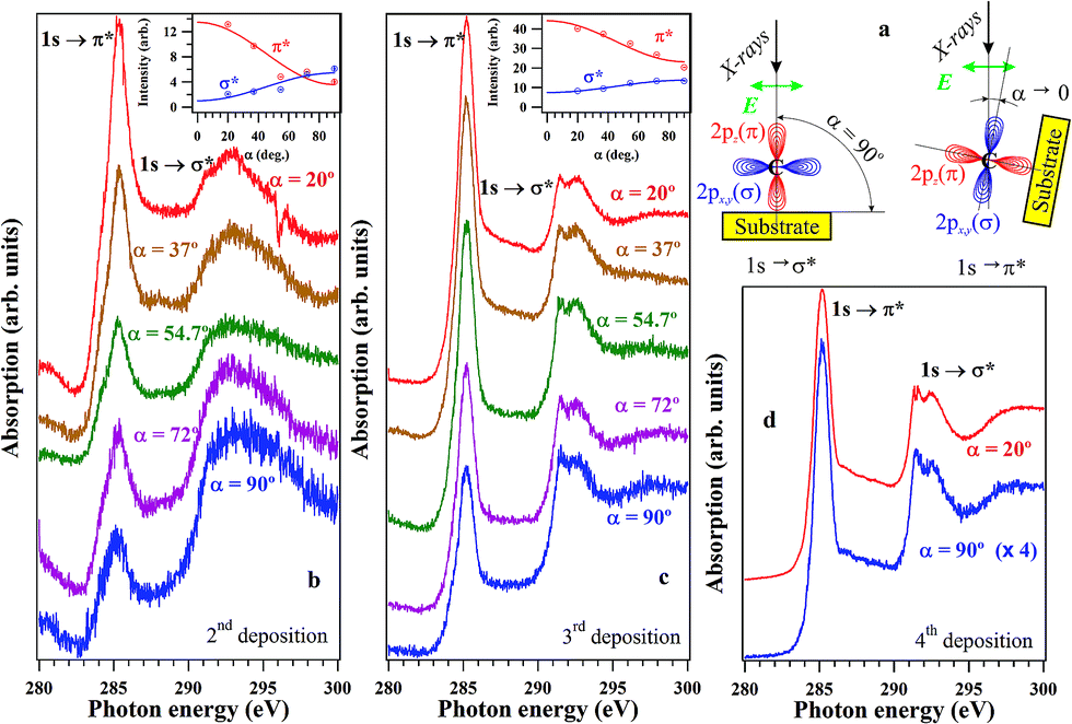 | ||
| Fig. 2 Carbon K near-edge absorption fine structure (NEXAFS) of the last three carbon depositions. (a) Represents the scheme of the experiments, with the definition of the angle α, the direction of the light polarization (E, in green), and a sketch of in-plane 2px,y and out-of-plane 2pz orbitals; NEXAFS spectra of the 2nd deposition (b) and of the 3rd deposition (c), for several angles α. NEXAFS on the 3rd deposition (d) was recorded just in normal incidence (α = 90°) and grazing incidence (α = 20°). Since these two spectra are similar, spectra at intermediate angles were not recorded. Inserts in (b) and (c) are fits of the intensities of σ* and π* resonances with a + bsin2α and a + bcos2α, respectively. | ||
Conclusion
Non-interacting carbon layers are formed on PZT without influencing the P(+) polarization of the ferroelectric (their sticking on the surface seems even to be favoured by the existence of this polarization) and exhibit 2D behaviour up to a few (2–3) atoms per non-primitive unit surface cell (of area a2). A side effect which needs to be investigated in more detail is the quenching of the Pb signal, which is probably due to the Pb migration inside the layer, but other final state effects should also be considered. This effect needs also to be investigated by photoelectron spectroscopy at different photon energies, different deposition temperatures, etc.Experimental methods
General aspects
(10 nm) PZT/(5 nm) SrRuO3/SrTiO3(001) and on Pt(001) films were prepared by pulsed laser deposition (PLD),17,18 and the X-ray absorption and photoemission experiments (including carbon deposition) were performed on the SuperESCA beamline at the synchrotron radiation facility Elettra, Trieste, Italy. All spectra are normalized with respect to the current recorded on the last refocusing mirror (40 nA reference value). The base pressure of the photoemission setup is in the range of low 10−8 Pa. The photon energies for different core levels (260 eV for Pb 4f and Zr 3d, 600 eV for O 1s and Ti 2p, and 400 eV for C 1s) were chosen in order to record spectra with similar kinetic energies and surface sensitivity. For NEXAFS, the C KLL Auger intensity is recorded vs. variable photon energy.Data analysis
Photoemission from PZT is analyzed by ‘deconvolution’ using Voigt lines and thresholds.26 The broadening of spin–orbit split lines of a doublet was the same, with the exception of Ti 2p, where the 2p1/2 line is considerable broader than the 2p3/2 line, owing to additional Coster–Kronig decay channels.37 The C 1s spectra for the first two depositions were better fitted by using two Voigt profiles, whereas the C 1s spectra for last two depositions were better simulated with a linear combination of Doniach–Šunjić lineshapes and gaussian profile.27Acknowledgements
Experimental support from Dr Silvano Lizzit and Dr Paolo Lacovig is greatly acknowledged. Access to the Elettra synchrotron radiation facility was possible through the Long Term Project 20130333. This work was funded by the Romanian UEFISCDI funding agency through Contracts PN-II-ID-PCCE-2011-2-0006 and PN-II-RU-TE-2014-4-0456.Notes and references
- F. Schwierz, Nat. Nanotechnol., 2010, 5, 487–496 CrossRef CAS PubMed.
- K. F. Mak, C. H. Lui, J. Shan and T. F. Heinz, Phys. Rev. Lett., 2009, 102, 256405 CrossRef PubMed.
- X. Hong, A. Posadas, K. Zou, C. H. Ahn and J. Zhu, Phys. Rev. Lett., 2009, 102, 136808 CrossRef CAS PubMed.
- X. Hong, K. Zou, A. M. DaSilva, C. H. Ahn and J. Zhu, Solid State Commun., 2012, 152, 1365–1374 CrossRef CAS.
- A. Rajapitamahuni, J. Hoffman, C. H. Ahn and X. Hong, Nano Lett., 2013, 13, 4374–4379 CrossRef CAS PubMed.
- X. Hong, J. Hoffman, A. Posadas, K. Zou, C. H. Ahn and J. Zhu, Appl. Phys. Lett., 2010, 97, 033114 CrossRef.
- E. B. Song, B. Lian, S. M. Kim, S. J. Lee, T.-K. Chung, M. S. Wang, C. F. Zeng, G. Y. Xu, K. Wong, Y. Zhou, H. I. Rasool, D. H. Seo, H.-J. Chung, J. S. Heo, S. N. Seo and K. L. Wang, Appl. Phys. Lett., 2011, 99, 042109 CrossRef.
- N. H. Park, H. Y. Kang, J. G. Park, Y. R. Lee, Y. J. Yun, J.-H. Lee, S.-G. Lee, Y. H. Lee and D. S. Suh, ACS Nano, 2015, 9, 10729–10736 CrossRef CAS PubMed.
- C. Baeumer, S. P. Rogers, R. J. Xu, L. W. Martin and M. S. Shim, Nano Lett., 2013, 13, 1693–1698 CAS.
- J. H. Park, W. C. Mitchel, L. Grazulis, H. E. Smith, K. Eyink, J. J. Boeckl, D. Tomich, S. D. Pacley and J. E. Hoelscher, Adv. Mater., 2010, 22, 4140–4145 CrossRef CAS PubMed.
- M. Batzill, Surf. Sci. Rep., 2012, 67, 83–115 CrossRef CAS.
- Y. Dedkov and E. Voloshina, J. Phys.: Condens. Matter, 2015, 27, 303002 CrossRef PubMed.
- R. Balog, B. Jørgensen, L. Nilsson, M. Andersen, E. Rienks, M. Bianchi, M. Fanetti, E. Lægsgaard, A. Baraldi, S. Lizzit, Z. Sljivancanin, F. Besenbacher, B. Hammer, T. G. Pedersen, P. Hofmann and L. Hornekær, Nat. Mater., 2010, 9, 315–319 CrossRef CAS PubMed.
- S. Lizzit, R. Larciprete, P. Lacovig, M. Dalmiglio, F. Orlando, A. Baraldi, L. Gammelgaard, L. Barreto, M. Bianchi, E. Perkins and P. Hofmann, Nano Lett., 2012, 12, 4503–4507 CrossRef CAS PubMed.
- I. Krug, N. Barrett, A. Petraru, A. Locatelli, T. O. Mentes, M. A. Niño, K. Rahmanizadeh, G. Bihlmayer and C. M. Schneider, Appl. Phys. Lett., 2010, 97, 222903 CrossRef.
- F. Chen and A. Klein, Phys. Rev. B: Condens. Matter Mater. Phys., 2012, 86, 094105 CrossRef.
- N. G. Apostol, L. E. Stoflea, G. A. Lungu, C. Chirila, L. Trupina, R. F. Negrea, C. Ghica, L. Pintilie and C. M. Teodorescu, Appl. Surf. Sci., 2013, 273, 415–425 CrossRef CAS.
- I. Pintilie, C. M. Teodorescu, C. Ghica, C. Chirila, A. G. Boni, L. Hrib, I. Pasuk, R. Negrea, N. G. Apostol and L. Pintilie, ACS Appl. Mater. Interfaces, 2014, 6, 2929–2939 CAS.
- L. E. Ştoflea, N. G. Apostol, L. Trupină and C. M. Teodorescu, J. Mater. Chem. A, 2014, 2, 14386–14392 Search PubMed.
- D. G. Popescu, M. A. Huşanu, L. Trupină, L. Hrib, L. Pintilie, A. Barinov, S. Lizzit, P. Lacovig and C. M. Teodorescu, Phys. Chem. Chem. Phys., 2015, 17, 509–520 RSC.
- M. A. Huşanu, D. G. Popescu, C. A. Tache, N. G. Apostol, A. Barinov, S. Lizzit, P. Lacovig and C. M. Teodorescu, Appl. Surf. Sci., 2015, 352, 73–81 CrossRef.
- N. G. Apostol, L. E Ştoflea, L. C. Tănase, I. C. Bucur, C. Chirilă, R. F. Negrea and C. M. Teodorescu, Appl. Surf. Sci., 2015, 354, 459–468 CrossRef CAS.
- L. Pintilie, C. Ghica, C. M. Teodorescu, I. Pintilie, C. Chirila, I. Pasuk, L. Trupina, L. Hrib, A. G. Boni, N. G. Apostol, L. E. Abramiuc, R. Negrea, M. Stefan and D. Ghica, Sci. Rep., 2015, 5, 14974 CrossRef CAS PubMed.
- L. Pintilie and M. Alexe, J. Appl. Phys., 2005, 98, 124103 CrossRef.
- L. Pintilie, I. Boerasu, M. J. M. Gomes, T. Zhao, R. Ramesh and M. Alexe, J. Appl. Phys., 2005, 98, 124104 CrossRef.
- C. M. Teodorescu, J. M. Esteva, R. C. Karnatak and A. El Afif, Nucl. Instrum. Methods Phys. Res., Sect. A, 1994, 345, 141–147 CrossRef CAS.
- J. J. Joyce, M. Del Giudice and J. H. Weaver, J. Electron Spectrosc. Relat. Phenom., 1989, 49, 31–45 CrossRef CAS.
- J. J. Yeh and I. Lindau, At. Data Nucl. Data Tables, 1985, 32, 1–155 CrossRef CAS.
- P. Hofmann, C. Søndergaard, S. Agergaard, S. V. Hoffmann, J. E. Gayone, G. Zampieri, S. Lizzit and A. Baraldi, Phys. Rev. B: Condens. Matter Mater. Phys., 2002, 66, 245422 CrossRef.
- A. B. Preobajenski, M. L. Ng, A. S. Vinogradov and N. Mårtensson, Phys. Rev. B: Condens. Matter Mater. Phys., 2008, 78, 073401 CrossRef.
- M. Iliut, C. Leordean, V. Canpean, C. M. Teodorescu and S. Astilean, J. Mater. Chem. C, 2013, 1, 4094–4104 RSC.
- J. Robertson, W. L. Warren, B. A. Tuttle, D. Dimos and D. M. Smyth, Appl. Phys. Lett., 1993, 63, 1519–1521 CrossRef CAS.
- S. Lizzit, G. Zampieri, L. Petaccia, R. Larciprete, P. Lacovig, E. D. L. Rienks, G. Bihlmayer, A. Baraldi and P. Hofmann, Nat. Phys., 2010, 6, 345–349 CrossRef CAS.
- P. Batson, Phys. Rev. B: Condens. Matter Mater. Phys., 1993, 48, 2608–2610 CrossRef CAS.
- O. Wessely, M. I. Katsnelson and O. Eriksson, Phys. Rev. Lett., 2005, 94, 167401 CrossRef CAS PubMed.
- E. Voloshina, R. Ovcharenko, A. Shulakov and Y. Dedkov, J. Chem. Phys., 2013, 138, 154706 CrossRef PubMed.
- D. Luca, C. M. Teodorescu, R. Apetrei, D. Macovei and D. Mardare, Thin Solid Films, 2007, 515, 8605–8610 CrossRef CAS.
Footnote |
| † Electronic supplementary information (ESI) available: SI-1 describes in more details the experimental procedures and shows photoemission overview scans for all surfaces investigated. SI-2 presents all the series of XPS spectra recorded during the cleaning procedure of the PZT layer, together with their analysis by curve fitting. SI-3 presents XPS spectra and their deconvolutions for several stages of carbon deposition. SI-4 presents time-resolved spectra during annealing of the 1st carbon layer and during the further carbon deposition. SI-5 presents carbon K NEXAFS from a graphene layer grown on Pt(001). See DOI: 10.1039/c6ra12910b |
| This journal is © The Royal Society of Chemistry 2016 |