
 Open Access Article
 This Open Access Article is licensed under a Creative Commons Attribution-Non Commercial 3.0 Unported Licence
Effect of oxygen pressure on structure and ionic conductivity of epitaxial Li0.33La0.55TiO3 solid electrolyte thin films produced by pulsed laser deposition
K. Kamala
Bharathi†
*ab,
H.
Tan†
ac,
S.
Takeuchi
a,
L.
Meshi
ad,
H.
Shen
a,
J.
Shin
b,
I.
Takeuchi
b and
L. A.
Bendersky
*a
aMaterial Measurement Laboratory, National Institute of Standards and Technology, Gaithersburg, Maryland 20899, USA. E-mail: kkamalabharathi@gmail.com; leoben@nist.gov
bDepartment of Materials Science and Engineering, University of Maryland, College Park, Maryland 20742, USA
cTheiss Research, La Jolla, CA 92037, USA
dDepartment of Materials Engineering, Ben Gurion University of the Negev, POB 653, Beer Sheva 84105, Israel
First published on 22nd June 2016
Abstract
We report on the ionic conductivity of Li0.33La0.55TiO3 (LLTO) epitaxial films grown on the (100) and (111) surfaces of single crystal SrTiO3 (STO) substrates at different oxygen partial pressures (from 1.33 to 26.66 Pa). The films are intended for use as solid electrolytes for all-solid-state Li-ion batteries, and the epitaxial growth for modeling the electrolyte single crystal properties. The LLTO films overall exhibit formation of the perovskite-based orthorhombic structure with the epitaxial cube-on-cube orientation for both (100)STO and (111)STO substrates. Room temperature ionic conductivity of the LLTO films measured by impedance spectroscopy slightly decreases with the oxygen partial pressure changing from 1.33 to 26.66 Pa and is in the range of 10−4 to 10−5 S cm−1. Complex impedance plots at different temperatures indicate that the conductivity in these epitaxial films is predominantly an intrinsic bulk property and exhibits distribution of relaxation time. Activation energies (Ea) for all the films were calculated employing the Arrhenius relationship and are between 0.30 eV and 0.40 eV, agreeing well with the reported values of bulk materials. Systematic difference in ionic conductivity between the (100)STO and (111)STO films is understood as being related to the difference in distribution of a “bottleneck” diffusion path. The measured conductivity of LLTO films indicates that these films can be used as a solid electrolyte in all-solid-state batteries.
Introduction
Li-ion batteries are extensively used in a wide range of electrical and electronic devices and in most of the electrical vehicles.1–5 All-solid-state batteries composed of positive/negative electrodes and electrolyte in solid form could offer significant advantages compared to the conventional Li-ion batteries, such as improved safety, absence of leakage and shorting related issues, and higher energy and power density.6–8 The development of thin film based all-solid-state batteries with high ionic conducting electrolytes would produce an enormous breakthrough in miniaturization of electronic devices. Searches for solid electrolyte materials with high ionic conductivity and stable against Li metal or cathode materials have been carried out by a number of research groups.9–12 Those solid electrolytes included conducting polymers, oxides, sulfides and other materials.13,14 Solid Li-ion conductors in polycrystalline and amorphous forms were investigated but most of them failed as a solid electrolyte due to the thermal instability and lower decomposition potentials.15,16 Among the oxide solid electrolytes, perovskite-based Li3xLa2/3−xTiO3 (LLTO) has been extensively studied due to its high lithium ion conductivity at room temperature (RT);17–24e.g., for composition Li0.35La0.55TiO3 the highest ionic conductivity of 10−3 S cm−1 in bulk form was demonstrated. However, LLTO has a number of issues as a solid electrolyte, such as instability against Li metal (reduction of Ti4+ to Ti3+) and reduced ionic conductivity due to the grain boundaries contribution to the total conduction.17–24 Measuring conductivity of epitaxial oriented LLTO films should allow to minimize the grain boundary effects, which is dominant for polycrystalline films. Also, anisotropy of Li-ion diffusion can be studied and optimized by using epitaxial films of different crystallographic orientations.In the present study we have successfully grown epitaxial LLTO thin films on STO (100) and (111) substrates at different oxygen partial pressures; the films are intended for fundamental studies of the films' behavior as solid electrolytes in different crystallographic orientations and with different crystallographic surfaces for all-solid Li-ion batteries. In the present work we intended to achieve the controlled growth with desired crystal structure and film's morphology, as well as dielectric property and ionic conductivity of the LLTO films by using pulsed laser deposition (PLD) technique, which included studying the effect of changing oxygen partial pressure during the growth. Detailed analysis of how temperature and oxygen partial pressure (PO2) affect ac and dc electrical properties and their correlation to the structural properties is presented in this paper.
Experimental section
LLTO thin films were deposited using PLD on single crystal STO substrates with two surfaces, (100) and (111) (square shape, approximately 0.5 × 0.5 cm). Before deposition the STO substrates were cleaned with acetone and ethanol for 15 minutes each in a sonicator.25,26 All the substrates were thoroughly dried with nitrogen before introducing them into the deposition chamber, which was initially evacuated to a base pressure of ∼5.33 × 10⁻⁴ Pa. A KrF laser (wavelength 248 nm) was employed whose repetition rate was 10 Hz and laser energy was 100 mJ per pulse. Li0.33La0.55TiO3 ceramic pellet was prepared employing solid-state synthesis method and used as a target for all the thin film depositions. The LLTO target was placed on a target holder, which is 6.8 cm away from the substrates. Before each deposition, the targets were pre-sputtered for 5 min to eliminate the impurities on the surface. All the films were deposited for 20 minutes at 1073 K temperature of the substrate, 1.33, 6.66, 13.33 and 26.66 Pa oxygen pressures.Phase and orientation characteristics of LLTO films were evaluated by a 4-axes Bruker D8 Discover X-ray diffractometer‡ (XRD). Ionic conductivity measurements were measured employing an ac impedance spectroscopy (Solartron 1260 impedance analyzer) at a frequency range from 1 Hz to 10 MHz. For the ac impedance measurements, Au parallel plate electrodes were deposited on the top surface of the LLTO film employing a chemical vapor deposition (CVD) technique. It was reported that conductivity of STO substrates can be affected by films' growth conditions, such as temperature and oxygen partial pressure;27,28e.g., Kalabukhov et al.28 have studied LaAlO3 grown on STO substrates at various oxygen partial pressures and temperatures and found that the sheet resistance of STO substrates annealed at very low pressures (1.3 × 10⁻⁷ Pa) 800 °C exhibits high conductivity, whereas treating at high pressures (6.66 Pa and above) and 800 °C results in insulating nature. To eliminate the possible contribution of STO substrates' conductivity to the total conductivity measurements, we have carried out the conductivity measurements on bare STO (100) and (111) substrates (0.05 cm thick substrates) after treating the films to growth experimental conditions (800 °C, 1.33 Pa). RT conductivity of the bare STO substrates was found to be of the order of 10−8 S cm−1 before the treatment and 10−10 S cm−1 after, thus two order of magnitude decrease in the STO surface conductivity. Since this conductivity is five orders of magnitude less than that of the LLTO films, the contribution of STO to the total conductivity can be safely neglected.
The morphology of exactly the same films was investigated by scanning electron microscopy (SEM). Electron-transparent cross-sectional transmission electron microscopy (TEM) lamellas were prepared by focus ion beam (FIB) (FEI Nova 600 NanoLab™). Carbon and Pt were coated on the LLTO film surface in advance to protect it against ion damage. The lamellas were milled and cleaned by Ga ions to typically 50 nm in thickness for good electron transparency. High-angle annular dark field scanning transmission electron microscopy (HAADF-STEM) investigation was performed on the prepared lamellas using a probe-corrected FEI Titan 80-300 microscope operating at 300 KV. The probe is typically corrected to provide a spatial resolution of 0.1 nm. The probe convergence angle is 24 mrad and the HAADF inner and outer collection angles are 70 mrad and 400 mrad respectively. Electron diffraction was performed on another FEI Titan 80-300 microscope operating at 300 kV.
Results and discussion
Fig. 1 shows out-of-plane XRD patterns taken from the LLTO films grown on the STO (100) and (111) substrates at four different partial PO2 pressures, 1.33, 6.66, 13.33 and 26.66 Pa PO2 at 1073 K. The few peaks, which appear as satellites of the STO peaks imply that the films have grown epitaxially on both the STO (100) and (111) surfaces, with cube-on-cube orientation relationship between perovskite (p) STO and LLTO. Electron diffraction results shown below suggest that LLTO is the ordered orthorhombic perovskite-based phase, as reported in the literature.17–20 With the substrate STO (100) peak as a reference, the out-of-plane lattice parameter (OPL) LLTO films grown at various PO2 can be precisely measured (inset of Fig. 1). Lattice parameter decreases with increasing PO2 and then some increase is observed for the films grown at 26.66 Pa. The observed OPL changes could be an indication that PO2 during the films' growth affect the number of oxygen vacancies, and accordingly the Ti ionic state, which will be discussed later. | ||
| Fig. 1 XRD patterns of LLTO films grown on STO (100) and (111) substrates at 1.33, 6.66, 13.33 and 26.66 Pa (a) to (h), indication the formation of perovskite structure. Inset of (h) shows the variation of c axis lattice parameter with PO2. | ||
Fig. 2 shows top view SEM images of LLTO films grown at various PO2 on STO (100) and (111) substrates, demonstrating significant differences in the surface morphology of the films. The film grown at 1.33 Pa on STO (100) shows the presence of faceted islands (50–150 nm in size) on its surface (Fig. 2a). The film grown at 1.33 Pa on STO (111) surface also shows islands on the surface but without particular facets that would be related to the substrate's orientation (Fig. 2b). On the other hand, the uniform contrast of the films grown at 6.66 Pa on both STO (100) and STO (111), Fig. 2c and d, suggests extremely flat surfaces. Small randomly distributed particles (30–70 nm) are also observed on the surface of films grown at 13.33 Pa PO2, Fig. 2e and f. The sample grown at 26.66 Pa on STO (100), Fig. 2g, has relatively flat surface with small darker spots (∼40 nm), while the sample grown at the same oxygen pressure on STO (111) substrate exhibits domains (100–150 nm) with very obvious triangular facets (see Fig. 2h). Those facets are {100} side planes with top (111) of the perovskite LLTO, according to the identified cube-on-cube epitaxial relationship with STO (111) substrate. It seems that at this experimental condition the faceted morphology was by growth and coalescence of island with lowest surface energy. These noticeable morphology changes imply that surface energies and growth modes of LLTO are remarkably sensitive to the oxygen pressure during the PLD growth.
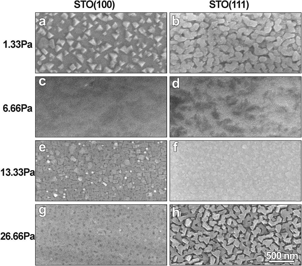 | ||
| Fig. 2 (a) to (h) shows top view SEM images of the LLTO films grown at various PO2 on STO (100) and (111) substrates, illustrating the dramatically different morphology. | ||
For the more in-depth investigation of the films' microstructure and morphology, TEM and STEM investigation of cross-sectioned samples was performed. For this purpose the lamellas were cut by FIB along the [010] direction of the STO substrate for films deposited on STO (100) and along the STO [110] direction for films deposited on STO (111) substrates; STEM images of all cross-sections are presented in Fig. 3. The film thicknesses for all the 8 samples vary between 240 nm and 60 nm (Table 1). The films are thinner for the samples deposited at higher oxygen pressure, which could be the result of the plasma plume condition when ions reaching the substrate are more strongly scattered at higher oxygen density/pressure. That explanation also agrees with the fact that the film thickness is very similar for the samples deposited at the same oxygen pressure on different substrate's orientations. The only difference is 26.66 Pa depositions, showing that for STO (111) substrate the film is twice thicker than the film deposited on STO (100); the difference might be explained by the presence of unfilled spaces between isolated faceted islands for the STO (111) film (Fig. 2h and 3h) the volume of which was compensated by the extra thickness.
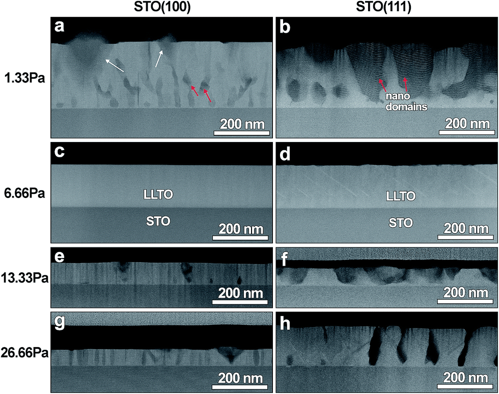 | ||
| Fig. 3 (a) to (h) present STEM cross-sectional view of the LLTO films grown at various PO2 on STO (100) and (111) substrates. | ||
| P(O2) Pa | t (nm) | σ (at RT) S cm−1 | E a (eV) | R g (Ω) | C g (F) | |||||
|---|---|---|---|---|---|---|---|---|---|---|
| STO (100) | STO (111) | STO (100) | STO (111) | STO (100) | STO (111) | STO (100) | STO (111) | STO (100) | STO (111) | |
| 1.33 | 240(±3) | 230(±4) | 4.3 × 10⁻⁵ | 5.63 × 10⁻⁵ | 0.34 | 0.34 | 7.1 × 10⁸ (353 K) | 1.8 × 10⁸ (358 K) | 2.4 × 10⁻¹¹ (353 K) | 2.6 × 10⁻¹¹ (358 K) |
| 2.66 | 155(±0.4) | 155(±1) | 3.08 × 10⁻⁵ | 5.37 × 10⁻⁵ | 0.38 | 0.34 | 6.2 × 10⁸ (362 K) | 6.2 × 10⁸ (273 K) | 2.7 × 10⁻¹¹ (362 K) | 6.6 × 10⁻¹¹ (273 K) |
| 13.33 | 81.6(±1) | 70(±2) | 3.01 × 10⁻⁵ | 5.01 × 10⁻⁵ | 0.33 | 0.40 | 3.6 × 10⁸ (353 K) | 3.3 × 10⁸ (353 K) | 3.6 × 10⁻¹¹ (353 K) | 2.8 × 10⁻¹¹ (353 K) |
| 26.66 | 61.2(±1) | 145(±2) | 3.02 × 10⁻⁵ | 4.95 × 10⁻⁵ | 0.40 | 0.40 | 4.3 × 10⁷ (473 K) | 2.0 × 10⁷ (423 K) | 2.2 × 10⁻¹¹ (473 K) | 4.2 × 10⁻¹¹ (423 K) |
Cross-sectional STEM images in Fig. 3 show contrast variations for the films deposited at 1.33, 13.33 and 26.66 Pa; such variations reflect differences in average Z (density), and to lesser degree – variation in diffraction condition. Using classical electron crystallography and high-angle annular dark field scanning transmission electron microscopy (HAADF-STEM) methods these films were characterized as possessing variety of 2D and 3D structural defects, including micro-domains and inclusions of secondary unknown phase. These results will be published as a separate paper which is currently in preparation. However some conclusions from that study relevant to understanding electrical behavior of the film, which is the focus of the current paper, are summarized below.
Selected area (SAED) and nanobeam (NBD) electron diffraction patterns taken from the prevailing phase appearing in the grown LLTO layers are shown in Fig. 4. These patterns are indexed in terms of the basic cubic perovskite (p) structure (with ap lattice parameter). Such indexing underlines the superstructural reflections (marked by arrows to guide the eye) appearing in all patterns. These additional reflections suggest ordering of the perovskite structure by forming the orthorhombic (o) phase (either Cmmm, ao ≈ 2ap; bo ≈ 2ap; co ≈ 2ap; or Pmma, ao ≈ √2ap; bo ≈ 2ap; co ≈ √2ap, as reported earlier17–20); the phase ordering combines chemical (separation of Li and La to tetragonal layering) and displacive (rotation of TiO6 octahedra) orderings. It was noted that this phase contains high amount of structural defects. The lowest amount of defects was observed in the LLTO layers deposited at 6.66 Pa PO2. SAED taken from these films (see Fig. 4c and d) can be easily indexed in terms of either of the mentioned above orthorhombic phases (superstructural reflections are marked by blue arrows on Fig. 4c). Other films exhibited SAED which can be indexed as a superposition of 90°-oriented microdomains of the orthorhombic phase (see red and blue arrows on Fig. 4a, for example). The alignment of the LLTO and STO diffraction spots demonstrate epitaxial growth of the films with cube-on-cube orientation relationship LLTO (100)//STO (100) and LLTO (001)//STO (001) for both STO (100) and STO (111) substrates (Fig. 4c and d, for instance).
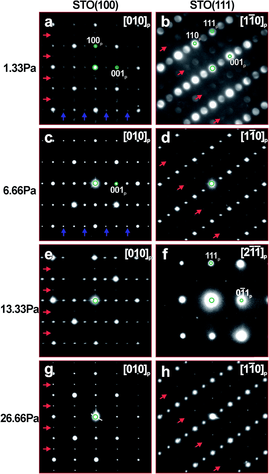 | ||
| Fig. 4 Electron diffraction patterns of the dominant LLTO phase grown in the films as a function of O2 pressure and STO substrate orientation. The patterns are indexed in terms of basic perovskite structure and superstructural reflections are marked by arrows. Due to the existence of 90° oriented domains, additional reflections appear. On the left panel, red and blue arrows mark the rows of superstructural reflections appearing from different sets of perpendicular domains. At image (b) nanobeam electron diffraction pattern is presented and not SAED as in other images. | ||
The LLTO films grown at 1.33 Pa, Fig. 3a and b, show regions of darker contrast embedded into a phase of a lighter contrast. Although SAED patterns from the lighter dominant phase, Fig. 4a and b, where indexed in terms of mentioned orthorhombic LLTO, darker regions belong to a different, not perovskite-related X phase which is in specific orientation relationship with the orthorhombic LLTO phase. Based on the numerous SAED patterns taken at different orientations of the X phase, we suggest that this new phase is hexagonal, with approximate lattice parameters of a = 0.95 nm, c = 1.0 nm, or orthorhombic, with approximate lattice parameters of a = 1.02 nm, b = 1.64 nm and c = 1.0 nm. To the best of our knowledge, such phase was not reported neither for the Li–La–Ti–O nor for other related systems.
The LLTO films grown at 13.33 and 26.66 Pa, although showing alternating variations in contrast, see Fig. 3e–h, according to the SAED patterns shown in Fig. 4e–h, have predominately the orthorhombic LLTO phase in the same orientation relationship with STO substrates as discussed above. The darker regions seen in lower magnification were recognized as thinner part of the films. Presence of such thinner areas is the result of overlapping between the film's materials and empty spaces between the grown and not completely merged islands. This suggestion is in line with the SEM images presented in Fig. 2.
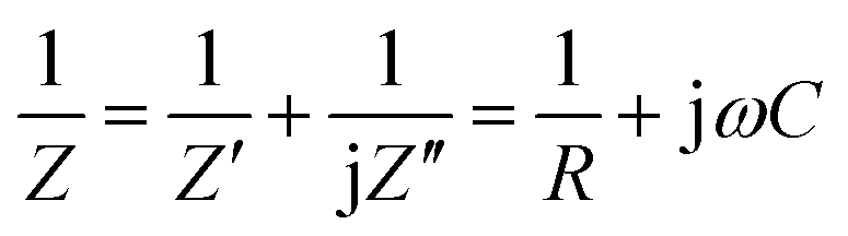
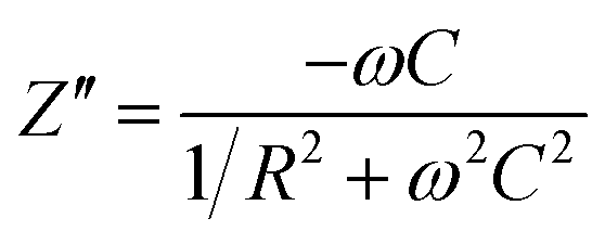
For the conductivity measurements, parallel plates of Au electrodes were deposited on the surface of LLTO films (inset in Fig. 5a) by chemical vapor deposition. The impedance of LLTO films at temperatures ranging from RT to 548 K was measured in the frequency range of 1 Hz to 10 MHz. Impedance of a LLTO material can be expressed as of a parallel circuit:29,30
 | (1) |
 | (2) |
 | (3) |
 | ||
| Fig. 5 Frequency variation of real part of impedance (Z′) at different temperatures of LLTO film grown on STO (100) and (111) at 1.33 Pa (a) and (b). Frequency variation of imaginary part of impedance (Z′′) at different temperatures of LLTO film grown on STO (100) and (111) at 1.33 Pa (c and (d)). | ||
Fig. 5a and (b) show variation of Z′ with frequency (at different temperatures) for LLTO on STO (100) and STO (111) films grown at 1.33 Pa. The LLTO films grown on STO (100) and (111) exhibit decreasing Z′ with increasing frequency at all the temperatures, show that the conductivity of the LLTO increases both with the frequency and temperature increases; both dependencies can be understood as increase in hopping of Li ions (from 10 kHz to 10 MHz). Fig. 5c and (d) shows the frequency variation of Z′′ for the same LLTO films (grown at 1.33 Pa) at different temperatures. Frequency dependent Z′′ is seen to exhibit broad asymmetric Debye peaks due to the resonance of Li ion hopping frequency with the applied ac field at those frequencies (10 to 1 kHz and 100 to 6 kHz for the films grown on STO (100) and (111) substrates respectively), indicating the existence of relaxation process in the LLTO films. With increasing temperature, dielectric loss from the resistive part of LLTO films decreases, which resulted in the decrease in Z′′ part.
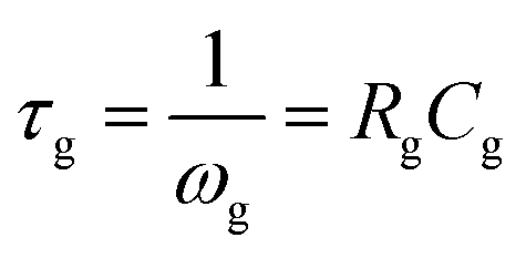
Fig. 6 and 7 shows complex impedance plots (real (Z′) versus imaginary (Z′′) part of impedance) for LLTO film grown on STO (100) and (111) substrates at 1.33, 6.66, 13.33 and 26.66 Pa; the figures present results measured at different temperatures (from RT to 548 K). At all the temperatures, single semi-circle is observed for LLTO films grown at different PO2. The radius of the semicircle decreases with increasing temperature due to increase in ionic conductivity of the film. The single semicircle in complex impedance plots for ionic conductors is usually accounted for the predominant contribution from the bulk of grains to the resistance and capacitance. The grain boundary contribution (which usually appear as a semi-circle or tail at higher frequencies31) to the R and C could not be resolved at all the temperatures in the LLTO films. Impedance (Z) due to bulk conduction of LLTO films can be expressed as29,30
| 1/Z = 1/Rg + jωCg | (4) |
 | (5) |
 | ||
| Fig. 6 Complex impedance plot of LLTO films grown at 1.33, 6.66, 13.33 and 26.66 Pa on STO (100) substrates (a) to (d). | ||
 | ||
| Fig. 7 Complex impedance plot of LLTO films grown at 1.33, 6.66, 13.33 and 26.66 Pa on STO (111) substrates (a) to (d). | ||
Relaxation time for LLTO films at different temperatures is seen to lie between 40 and 0.8 ms. Semi-circles obtained for the LLTO film at various temperatures can be represented by a RC electric circuit shown in inset of Fig. 7. In this equivalent circuit, Rg represents the conductive path and a given resistor in a circuit accounts for the bulk conductivity of the LLTO film. Space charge polarization regions are described as a capacitor (Cg) or a leaky capacitor, constant phase element (CPE) in the circuit. Cg is replaced by CPE, which accounts for the depressed semi-circle in the complex impedance plot and non-ideal Debye case for the present LLTO electrolyte thin films. In the present case, occurrence of inclined straight line in the lower frequency region is not clearly seen, indicating that the contributions from the electrode–electrolyte interface to the total conductivity do not seem to have much significance on the ionic conductivity of the LLTO films.
In-plane dc ionic conductivity of LLTO films are calculated using this relationship:33
| σin-plane = d/Rtl | (6) |
σdc = σ0![[thin space (1/6-em)]](https://www.rsc.org/images/entities/char_2009.gif) exp(−Ea/kBT) exp(−Ea/kBT) | (7) |
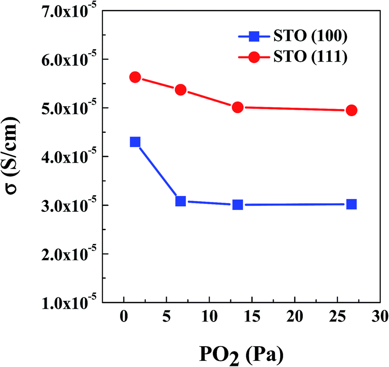 | ||
| Fig. 8 300 K conductivity as a function of PO2 for the LLTO films grown on STO (100) and (111) substrates. Decreasing ionic conductivity with increasing PO2 is clearly evident. | ||
The high Li-ion conductivity of the order of 10−3 S cm−1 at RT for LLTO oxide was suggested as its bulk property for the measurement of polycrystals (range of 10−5 to 10−4 S cm−1) after extraction of grain boundaries' effect.17 Direct measurement of the bulk conductivity was of interest to understand mechanism of diffusion/conductivity in LLTO. The single crystal Li0.35La0.55TiO2.94 was fabricated by the floating zone; impedance measurement showed 6.8 × 10⁻⁴ S cm−1 for current perpendicular to c-axis, and comparable 5.8 × 10⁻⁴ S cm−1 – parallel to c-axis.42 Later the same authors have shown that the grown crystal is not a mono-domain, but consisting 90°-oriented domains with the possible effect on conductivity of domain boundaries.43 Another approach to understand the LLTO bulk conductivity is through preparing and measuring single crystal films grown epitaxially. Such films of LixLa0.56TiO3 (x = 0.33 to 0.5) composition grown on STO and NdGaO3 by PLD, with multi-domain and single-domain structures, have shown conductivity one order of magnitude higher, 3.5 × 10⁻⁴ S cm−1, and activation energy similar to our films, 0.35 eV.44,45 From these works it was concluded that 90°-domain and antiphase boundaries are not predominantly resistive against the ionic conduction. Recently published work on Li0.33La0.56TiO3 prepared by different synthesis schedules demonstrated that in order to maximize the number of Li percolation pathways for higher ionic conductivity the mesoscopic structure of high-density 90°-domains is preferable; the results were corroborated by theoretical molecular dynamics simulations.46
It is difficult to compare results of our work with those published in literature for the following reasons: ionic conductivity of LLTO is sensitive to the composition of Li/La and to degree of ordering between Li, La and vacancies. Composition and order parameter of the films is difficult to measure with precision because of the low-Z of Li, whereas certain deviation from the target's composition and uncertainties in thermal history are expected. Nevertheless, the conductivity within the order of 10−5 S cm−1 for the STO (100) substrates, with the films consisting of 90° oriented domains of the orthorhombic LLTO, is very close to results obtained by Ohnishi et al.44,45 for the films deposited with the target of a similar Li0.33La0.55TiO3 composition on the NdGaO3 substrate; the results also prove that the STO substrate can be used without compromising electrical measurements. From Ohnishi et al. and our work, it can be claimed that the measured 10−4 to 10−5 S cm−1 conductivity is the bulk conductivity in the 〈001〉p direction of a perovskite (p) cubic cell, without noticeable distinction between the pseudo-cubic directions of the orthorhombic structure.
In order to understand the observed systematic differences in conductivity of LLTO films on STO (100) and STO (111) substrates, we analyze relative arrangements of the A-sites, which consist of Li, La and vacancies, and positions of the so-called bottlenecks.17 The “bottlenecks” are locations for the high ionic mobility path (with lowest energy barrier) that are formed by four adjacent TiO6 octahedra; the location is in 3d Wyckoff site of a perovskite Pm![[3 with combining macron]](https://www.rsc.org/images/entities/char_0033_0304.gif) m cell. In Fig. 9a a projection of the LLTO structure in [100]p direction shows only the A-site atom and the bottleneck positions (small circles); different colors distinguish the La-rich (green) and La-poor (red) (001)p layers. Directions of diffusing Li1+ ion through the nearest bottleneck into a vacant A-site are shown with curved arrows; the literature suggests that the diffusion confined to the (001) Li-rich plane is higher than in the out-off this plane direction. In the case of the LLTO films on STO (100) having mesoscopic 90°-domain structure, the percolation of Li ions in the film's plane during the conductivity measurements has to occur through different domain orientations, depends on distribution and size of the domains, and controlled by the domains of lower diffusion rate, as well as resistance of the domain's boundaries.
m cell. In Fig. 9a a projection of the LLTO structure in [100]p direction shows only the A-site atom and the bottleneck positions (small circles); different colors distinguish the La-rich (green) and La-poor (red) (001)p layers. Directions of diffusing Li1+ ion through the nearest bottleneck into a vacant A-site are shown with curved arrows; the literature suggests that the diffusion confined to the (001) Li-rich plane is higher than in the out-off this plane direction. In the case of the LLTO films on STO (100) having mesoscopic 90°-domain structure, the percolation of Li ions in the film's plane during the conductivity measurements has to occur through different domain orientations, depends on distribution and size of the domains, and controlled by the domains of lower diffusion rate, as well as resistance of the domain's boundaries.
 | ||
| Fig. 9 (a) Projection of the LLTO structure in [100]p (p-cubic perovskite) direction showing only the A-site atoms (red for higher Li and green for higher La) and positions of a bottleneck (small circles) in 3d Wyckoff site of a perovskite cell. (b) Sidewise projection in [−110]p direction of a structural slab with (111)p planes; the bottleneck sites are above (filled) and below (open) out the (111)p Li/La plane consisting of a mixture of A-sites from La-rich and Li-rich layers. (c) Projection of three (111)p planes of A-sites with the bottleneck sites above and below the central plane. | ||
For the LLTO films on STO (111) substrates, Li-ion diffusion along (111)p planes should be considered. In Fig. 9b a slice of such (111)p plane is shown; the slice includes three A-site planes (hatched circles – top plane, dashed circles – bottom plane) and positions of bottlenecks above and below central A-plane (solid circles). The planes have a mixture of A-sites from La-rich and Li-rich layers (red and green colors). As it is clear from the drawing, in-plane diffusing Li-ions have to move out of a single (111) A-site plane through a bottleneck site, either above or below the plane, as shown with the arrows. During this diffusion the activation energy is expected to be similar as for the cubic directions, which is in agreement with experimental results. However the possibility of diffusion jumps of the same energy either to upper or lower planes in the same electrical field provides higher probability of having an appropriate vacant site, which can explain the observed higher conductivity for the STO (111) films.
Conclusions
LLTO films were deposited on STO (111) and (100) substrates at different oxygen pressures. The structure, morphology and electrical properties of the LLTO films were studied systematically. Following conclusions were drawn based on presented results:(1) The effect of oxygen partial pressure PO2 during the PLD growth from the Li0.33La0.55TiO3 target and orientation of the STO substrates on ionic conductivity of LLTO films are reported.
(2) LLTO films can be grown epitaxially on both STO (100) and (111) substrates with unique cube-on-cube orientation relationship between perovskite STO and perovskite-based LLTO; the deposited phase has orthorhombic structure, either Cmmm or Pmma.
(3) With the exception of 1.33 Pa deposition, the films consist of a single phase; the best quality films are for the 6.66 Pa deposition. In the 1.33 Pa deposition, in addition to the orthorhombic phase – unknown X phase was revealed in the LLTO film.
(4) RT ionic conductivity of the LLTO films is of the order of 10−5 S cm−1 for both STO (100) and STO (111) substrates and varies slightly with PO2.
(5) Impedance studies as a function of temperature and frequency shows the existence of relaxation processes and their distribution in LLTO films.
(6) Conductivity of the LLTO films is predominantly due to the intrinsic bulk properties. Activation energy (Ea) for all the LLTO films is calculated to be around 0.30–0.40 eV, which is in good agreement with the reported and calculated activation energy values related to the Li-ion diffusion though the bottleneck channels.
(7) Systematic difference in anisotropic conductivity of the films grown on STO (100) and STO (111) substrates can be rationalized by the distribution of bottleneck sites above and below the A-site's of the (111) plane.
Acknowledgements
H. T. acknowledges support from the U.S. Department of Commerce, National Institute of Standards and Technology under financial assistance awards 70NANB14H027 and 70NANB15H025. S. T. thanks Dr G. Stafford in National Institute of Standards and Technology for his help with Lab View program and for useful discussions.References
- D. Liu, W. Zhu, J. Trottier, C. Gagnon, F. Barray, A. Guerfi, A. Mauger, H. Groult, C. M. Julien, J. B. Goodenough and K. Zaghib, RSC Adv., 2014, 4, 154–167 RSC.
- H. F. Xiang, Z. D. Li, K. Xie, J. Z. Jiang, J. J. Chen, P. C. Lian, J. S. Wu, Y. Yu and H. H. Wang, RSC Adv., 2012, 2, 6792–6799 RSC.
- J. B. Goodenough and Y. Kim, Chem. Mater., 2010, 22, 587–603 CrossRef CAS.
- Q. Huang, M. Yan and Z. Jiang, J. Power Sources, 2006, 156, 541–546 CrossRef CAS.
- Q. Huang, M. Yan and Z. Jiang, J. Solid State Electrochem., 2008, 12, 671–678 CrossRef CAS.
- S. Ohta, T. Kobayashi, J. Seki and T. Asaoka, J. Power Sources, 2012, 202, 332–335 CrossRef CAS.
- P. H. L. Notten, F. Roozeboom, R. A. H. Niessen and L. Baggetto, Adv. Mater., 2007, 19, 4564–4567 CrossRef CAS.
- L. Baggetto, R. A. H. Niessen, F. Roozeboom and P. H. L. Notten, Adv. Funct. Mater., 2008, 18, 1057–1066 CrossRef CAS.
- W. C. West, J. F. Whitacre, V. White and B. V. Ratnakumar, J. Micromech. Microeng., 2002, 12, 58–62 CrossRef CAS.
- K. Yamamoto, Y. Iriyama, T. Asaka, T. Hirayama, H. Fujita, C. A. J. Fisher, K. Nonaka, Y. Sugita and Z. Ogumi, Angew. Chem., 2010, 122, 4516–4519 CrossRef.
- Y. Li, J. T. Han, C. A. Wang, S. C. Vogel, H. Xie, M. Xu and J. B. Goodenough, J. Power Sources, 2012, 209, 278–281 CrossRef CAS.
- J. B. Goodenough and Y. Kim, Chem. Mater., 2010, 22, 587–603 CrossRef CAS.
- R. Mercier, J. P. Malugani, B. Fahys and G. Robert, Solid State Ionics, 1981, 5, 663–666 CrossRef CAS.
- J. H. Kennedy and Y. Yang, J. Electrochem. Soc., 1986, 133, 2437–2438 CrossRef CAS.
- R. Kanno and M. Murayama, J. Electrochem. Soc., 2001, 148, A742–A746 CrossRef CAS.
- R. Kanno, M. Murayama, T. Inada, T. Kobayashi, K. Sakamoto, N. Sonoyama, A. Yamada and S. Kondo, Electrochem. Solid-State Lett., 2004, 7, A455–A458 CrossRef CAS.
- Y. Inaguma, L. Chen, M. Itoh, T. Nakamura, T. Uchida, H. Ikuta and M. Wakihara, Solid State Commun., 1993, 86, 689 CrossRef CAS.
- S. Stramare, V. Thangadurai and W. Weppner, Chem. Mater., 2003, 15, 3974–3990 CrossRef CAS.
- Y. Harada, T. Ishigaki, H. Kawai and J. Kuwano, Solid State Ionics, 1998, 108, 407–413 CrossRef CAS.
- K. Kim, J. Kim, Y. Yoon and D. Shin, Met. Mater. Int., 2014, 20, 189–194 CrossRef CAS.
- X. Xiaoxiong, W. Zhaoyin, W. Jianguo and Y. Xuelin, Solid State Ionics, 2007, 178, 29–34 CrossRef.
- Y. Kai-Yun, F. Kuan-Zong and W. Moo-Chin, J. Appl. Phys., 2006, 100, 056102–056103 CrossRef.
- Z. Zheng, H. Fang, F. Yang, Z. K. Liu and Y. Wang, J. Electrochem. Soc., 2014, 161, A473–A479 CrossRef CAS.
- S. Kim, M. Hirayama, W. Cho, K. Kim, T. Kobayashi, R. Kaneko, K. Suzuki and R. Kanno, CrystEngComm, 2014, 16, 1044–1049 RSC.
- A. P. Dral, D. Dubbink, M. Nijland, J. E. ten Elshof, G. Rijnders and G. Koster, J. Visualized Exp., 2014, 94, 52209 Search PubMed.
- I. Hallsteinsen, M. Nord, T. Bolstad, P. E. Vullum, J. E. Boschker, P. Longo, R. Takahashi, R. Holmestad, M. Lippmaa and T. Tybell, Cryst. Growth Des., 2016, 16, 2357–2362 CAS.
- H. P. R. Rrederikse, W. R. Thurber and W. R. Hosler, Phys. Rev., 1964, 134, A442 CrossRef.
- A. Kalabukhov, R. Gunnarsson, J. Börjesson, E. Olsson, T. Claeson and D. Winkler, Phys. Rev. B: Condens. Matter Mater. Phys., 2007, 75, 121404 CrossRef.
- J. Smith and H. P. J. Wijn, Ferrites, Philips Technical Library, Eindhoven, Holland, 1965 Search PubMed.
- K. Kamala Bharathi, G. Markandeyulu and C. V. Ramana, Electrochem. Solid-State Lett., 2010, 13, G98–G101 CrossRef.
- M. A. Khan, R. Raza, R. B. Lima, M. Asharf Chaudhry, E. Ahmed, N. R. Khalid, G. Abbas, B. Zhu and N. Nasir, Ceram. Int., 2014, 40, 9775–9781 CrossRef CAS.
- L. N. Patro, K. Kamala Bharathi and N. Ravi Chandra Raju, AIP Adv., 2014, 4, 127139–127210 CrossRef.
- E. Navickas, M. Gerstl, F. Kubel and J. Fleig, J. Electrochem. Soc., 2012, 159, B411–B416 CrossRef CAS.
- K. Yang and J. Dho, J. Korean Phys. Soc., 2009, 55, 188–192 CrossRef CAS.
- J. W. Jeong, S. G. Lee, S. H. Jo, D. Y. Kim and T. H. Lee, J. Ceram. Process. Res., 2013, 14, 573–576 Search PubMed.
- V. Thangadurai and W. Weppner, Ionics, 2006, 12, 81–92 CrossRef CAS.
- J. Wei, D. Ogawa, T. Fukumura, Y. Hirose and T. Hasegawa, Cryst. Growth Des., 2015, 15, 2187–2191 CAS.
- S. Stramare, V. Thangadurai and W. Weppner, Chem. Mater., 2003, 15, 3974–3990 CrossRef CAS.
- C. Deviannapoorani, L. Dhivya, S. Ramakumar and R. Murugan, J. Power Sources, 2013, 240, 18–25 CrossRef CAS.
- A. A. Raskovalov, E. A. Ilina and B. D. Antonov, J. Power Sources, 2013, 238, 48–52 CrossRef CAS.
- J. Yoon, G. Hunter, S. Akbar and P. K. Dutta, Sens. Actuators, B, 2013, 182, 95–103 CrossRef CAS.
- Y. Inaguma, J. Yu, T. Katsumata and M. Itoh, J. Ceram. Soc. Jpn., 1997, 105, 548–550 CrossRef CAS.
- T. Tsurui, T. Katsumata and Y. Inaguma, Solid State Ionics, 2009, 180, 607–611 CrossRef CAS.
- T. Ohnishi, K. Mitsuishi, K. Nishio and K. Takada, Chem. Mater., 2015, 27, 1233–1241 CrossRef CAS.
- T. Ohnishi and K. Takada, Solid State Ionics, 2012, 228, 80–82 CrossRef CAS.
- C. Ma, Y. Cheng, K. Chen, J. Li, B. G. Sumpter, C.-W. Nan, K. L. More, N. J. Dudney and M. Chi, Adv. Energy Mater., 2016, 6, 160005 Search PubMed.
Footnotes |
| † Both authors (K. Kamala Bharathi and H. Tan) have contributed equally. |
| ‡ Certain commercial equipment, instruments, or materials are identified in this document. Such identification does not imply recommendation or endorsement by the National Institute of Standards and Technology, nor does it imply that the products identified are necessarily the best available for the purpose. |
| This journal is © The Royal Society of Chemistry 2016 |