Structural, compositional and functional properties of Sb-doped Mg2Si synthesized in Al2O3-crucibles

Tatsuya Sakamotoab, Alessia Famengo*c, Simona Barisonc, Simone Battistonc, Stefano Boldrinic, Alberto Ferrarioc, Stefania Fiamenic, Tsutomu Iidaa, Yoshifumi Takanashia and Monica Fabrizioc
aDepartment of Materials Science and Technology, Tokyo University of Science, 6-3-1, Niijuku, Katsushika-ku, Tokyo 125-8585, Japan
bJapan Society for the Promotion of Science (JSPS) Postdoctoral Research Fellow, Japan
cCNR-ICMATE, Corso Stati Uniti 4, 35127 Padova, Italy. E-mail: alessia.famengo@cnr.it

Received 2nd May 2016 , Accepted 12th August 2016

First published on 12th August 2016


Abstract

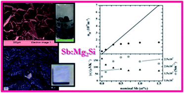
Magnesium silicide (Mg2Si) is a promising candidate for thermoelectric energy conversion due to its low toxicity, the abundance of its raw constituents and its low density, allowing manufacturing of light, sustainable and relatively cheap devices. Mg2Si needs to be doped in order to increase its efficiency, making this material competitive among materials operating in the intermediate temperature range. In this work, a synthesis procedure based on melting of the raw elements in easily available and cheap Al2O3 crucibles was developed to obtain polycrystalline Sb doped Mg2Si materials in a wide range of compositions. Powders from the crushed lumps were consolidated via spark plasma sintering and then thermally annealed to obtain dense pellets of Sb:Mg2Si with Sb = 0.0, 0.1, 0.3, 0.5, 0.7, 1.0 and 1.5 at%. The effects of Sb doping and of the synthesis and sintering technique on composition, morphology and stability of n-type Mg2Si are discussed. Transport properties (Seebeck coefficient, electrical and thermal conductivity, charge carrier density) were evaluated in order to elucidate the composition–property relationship within this material system and find the optimal doping amount to optimize its thermoelectric properties.


Introduction

Recently, the field of thermoelectric power generation is widening to large scale applications such as the conversion of waste heat in the automotive sector.1 In this field, research on suitable materials for thermoelectric generators (TEG) is prompted by the severe regulations on exhaust gas emissions. By using output from TE modules exploiting exhaust gases to power electrical components, a fuel economy improvement of almost 3% for a 2000 cm3 engine has been achieved.2

Among materials operating in the intermediate temperature range, lead-based tellurides such as PbTe alloys and heavy metal antimonides such as CoSb3 (ref. 1) possess the highest thermoelectric efficiency, which is related to the figure of merit image file: c6ra11367b-t1.tif where α is the Seebeck coefficient, and σ and k the electrical and thermal conductivity, respectively. However, the presence of toxic and/or scarcely available elements such as Te, Pb, Co together with the high density of lead tellurides and cobalt antimonides based compounds are a limit, especially for the automotive where lightweight materials with non-toxic components are preferable. In this point of view, Mg2Si is a promising candidate. It is a semiconductor with low density (1.98 g cm−3) adopting the anti-fluorite structure type with Si in face centered cubic positions and Mg in tetrahedral sites. Even if σ, α and k are not independent, in the antifluorite materials thermal conductivity k can be substantially reduced without degrading the electrical properties, providing high ZT values.3

To be an efficient thermoelectric, Mg2Si need to be doped or/and alloyed. In fact, increasing the number of charge carriers by doping lead to higher values of the electrical conductivity. Moreover, introducing heavier atoms in Mg2Si lattice can decrease the thermal conductivity because of the related phonon scattering effect. The value of the energy band gap of Mg2Si (0.77 eV (ref. 3 and 4)) ensures the separation between n-type and p-type carriers, thus doping will produce only a single carrier type. However, Mg2Si band gap is small enough allowing high versatility towards doping. The formation energies of n-doped Mg2Si are negative for substitution of As, P, Bi and Sb at the Si sites.5 Among group XV atoms, Bi is regarded as a good dopant because of its heavier atomic mass, effective in reducing thermal conductivity via phonon scattering mechanism. However, the solubility limit of Bi in Mg2Si is ≈0.7 at% (ref. 6) and the formation of secondary metallic phases such as Bi2Mg3 is quite common.7,8 On the other side, Sb possesses higher solubility on Mg2Si lattice (Mg3Sb2 is soluble in Mg2E, for E = Si, Ge, and Sn, up to 30%), as reported by Nolas et al.3 To the best of authors knowledge, the presence of secondary Mg3Sb2 phase on Sb doped Mg2Si was not clearly evidenced by standard characterization techniques.9,10

Therefore, Sb was chosen as dopant for Mg2Si, widening the Sb:Mg2Si composition range up to Sb = 1.5 at%.

The synthesis of magnesium silicide by melting techniques is not straightforward because of the difference between the boiling point of magnesium (1363 K), and the melting point of silicon (1703 K). Both elements have strong affinity for oxygen and the reaction must be conducted in an oxygen-free environment.11 Due to the reactivity of molten magnesium, crucibles usually employed must be made of expensive materials inert towards magnesium, for example Pt- or Ta-based crucibles. In this work a process to synthesize polycrystalline Sb-doped Mg2Si was developed employing Al2O3 crucibles which are cheap and easily available on an industrial scale.

The obtained lumps were then crushed and sintered via spark plasma sintering to obtain regular dense pellets of Sb:Mg2Si. Introducing a thermal annealing step after SPS sintering allows fabricating crack-free pellets with Sb up to 1.5 at%. In fact, as observed in a previous work by Fukushima,12 Sb:Mg2Si obtained by the same procedure but without the annealing step showed cracks for Sb > 0.5 at%.

The effects of Sb doping and of the synthesis and sintering techniques on composition, morphology and stability of n-type Mg2Si were discussed. Transport properties (Seebeck coefficient, electrical and thermal conductivity from 300 to 870 K and charge carrier density at room temperature) were measured in order to elucidate the composition–property relation within this material system and find the optimal doping amount for maximum ZT.

Experimental

Synthesis of polycrystalline Sb-doped Mg2Si

Raw Mg pieces (Nippon Thermochemical, 3 N), Si powders (Memc Electronic Materials, 6 N+), and Sb powders (Electronics and Materials, 6 N, under 5 μm) were molten in an Al2O3 crucible in Ar/H2 atmosphere with 5% H2. The mixture was heated at 1373 K and kept for 3 hours at this temperature. The quantity of each raw element was adjusted according to Mg2Si1−xSbx stoichiometry. The atomic percentages of Sb considered were 0.0, 0.1, 0.3, 0.5, 0.7, 1.0, 1.5. For example, Sb at% = 1.5 corresponds to Mg2Si0.955Sb0.045.

Consolidation of Sb-doped Mg2Si powders

Polycrystalline ingots were crushed in an alumina mortar under air and the resulting powders were sieved to collect three fractions of 75 μm, 45 μm, 25 μm grain size. 75–45 μm and 45–25 μm fractions were mixed together in a 1[thin space (1/6-em)]:[thin space (1/6-em)]1 weight ratio, placed in a graphite die and then sintered via SPS (Elenix “Ed-Pas III”) at 1143 K for 10 min keeping the pressure at 30 MPa under Ar (0.06 MPa). The sintered pellets were placed in a furnace and annealed at 973 K for 10 h under Ar atmosphere.

The annealed samples were cut using a wire saw in order to obtain regular round- and square shaped specimens for functional characterization. The density of the pellets was measured geometrically (Micrometer Mitutoyo MDC-1′′SFB and balance Sartorius BP61). The relative density was major than 97% for all sintered pellets.

Structural, morphological and compositional characterization

For each Sb:Mg2Si composition, 3 g of polycrystalline ingots were charged on a WC jar with 10 mL of hexane as dispersing medium and then pulverized in a planetary ball mill (Fritsch Pulverisette 6, 15′ milling at 350 rpm +15′ pause, cycle repeated 9 times) to reduce grain size (5 μm). X-ray diffraction (Philips PW 3710 X-ray diffractometer Koninklijke Philips, Bragg Brentano geometry, Cu Kα-40 kV, 30 mA) was performed on milled powders and on the materials after sintering process with a step width of 0.02 2θ at room temperature. The XRD patterns were fitted with Rietveld refinement using MAUD software to obtain information about phase content, lattice parameters, and theoretical density.13

The morphology and composition on fractured sintered pellet of Sb:Mg2Si were investigated by Field Emission Scanning Electron Microscopy (FE-SEM, Carl Zeiss GmbH) coupled with Energy Dispersive Spectroscopy (EDS, Oxford X-Max EDS system).

The quantification of Sb and of Al impurities on sintered Sb:Mg2Si was measured by Inductively Coupled Plasma Mass Spectrometry (ICP-MS Thermo Elemental X7-series) equipped with the Plasma Lab software package. Approximately 4 mg of a sintered pellet were dispersed in few mL of ultrapure water (17 MΩ) and a mixture of HCl[thin space (1/6-em)]:[thin space (1/6-em)]HNO3 = 3[thin space (1/6-em)]:[thin space (1/6-em)]1 (v/v, Sigma Aldrich and Alfa Aesar, respectively) was very slowly added dropwise (caution must be taken because Mg2Si powders react violently with acids releasing flammable gases) to dissolve the material. For instrument calibration two multielement standard solutions containing Al and Sb were used (SPI Science and Accustandard). Thermogravimetric analysis (TG) and differential scanning calorimetry (DSC), (SDT Q600-TA Instruments) were performed on milled powders from room temperature to 923 K in synthetic air (100 mL min−1) with a heating ramp of 5 K min−1.

Functional characterization

The thermal conductivity κ was calculated according to the formula κ = dρCp, where d (mm2 s−1) is the thermal diffusivity, ρ (g cm−3) is the density (geometrical), and Cp (J g−1 K−1) is the specific heat. The thermal diffusivity and specific heat of the samples were measured by a laser flash thermal diffusivity apparatus (Netzsch LFA 457 MicroFlash) from RT to 870 K on round pellets (diameter ≈ 12.7 mm). In particular, Cp was calculated using Netzsch Proteus analysis software, comparing the samples to a standard ceramic material Netszch Pyroceram 9606 with known Cp. The mean Cp value over all specimens was considered to calculate the thermal conductivity. The declared relative uncertainty of diffusivity measures and specific heat was 3% and 5% respectively.

The charge carrier concentration and the electrical resistivity were measured in the Van der Pauw configuration at RT on round pellets (diameter ≈ 12.7 mm, thickness ≈ 2 mm) using a permanent magnet (≈0.360 T), a sourcemeter (Keithley 2636) a nanovoltmeter (Keithley 2182) and measuring the magnetic field with a Hall-probe Gaussmeter (GM07, RS Scientific) with an estimated relative error of 10%. The Seebeck coefficient and electrical conductivity were simultaneously measured from RT to 870 K and verified with two apparatus (ULVAC ZEM-3 and a custom built apparatus14) with a relative uncertainty of 10%.

Results and discussion

Composition, structure and morphology of Sb:Mg2Si

Powder X-ray diffraction (XRD) of the polycrystalline ingots (Fig. 1) revealed the presence of cubic Fm3m Mg2Si [104864-ICSD] as major phase with no detectable MgO. This impurity was easily removed from ingots because MgO tends to segregate out the Mg2Si block during the melting synthesis process. Unreacted free Mg and Sb were not revealed for all the composition considered.
image file: c6ra11367b-f1.tif
Fig. 1 Powder X-ray diffraction pattern (black dots) of Mg2Si doped with nominal 0.0, 0.3, 0.5 and 1.5 Sb at% performed on polycrystalline lumps. The red solid line is Rietveld profile fitting.

Al Fm[3 with combining macron]m [44321-ICSD] and Si Fd[3 with combining macron]mS [41979-ICSD] were detected as secondary phases. In particular, Al content was estimated to be between 1.0 wt% and 5.4 wt%. The presence of Al could be attributed to the Al2O3 crucibles used in synthesis step. Considering the Ellingham diagram15 which plots the standard free energy of a reaction as a function of temperature, the free Gibbs energy for the reaction

image file: c6ra11367b-t2.tif
calculated from ΔG0 of the reactions
image file: c6ra11367b-t3.tif
is negative at 1373 K, the temperature of the synthesis process. Even if the equilibrium is shifted towards Mg2Si formation, it is reasonable to suppose that at this temperature liquid magnesium wetted the crucible and partially reacted with alumina to give Al and MgO. As already mentioned MgO was not detected in the XRD pattern because it segregated out of the polycrystalline ingot and easily removed.

The presence of free Si could be attributed to the fact that part of the Mg reacted with the crucible leaving an excess of this reactant. Considered the tendency of Mg2Si towards oxidation,16,17 segregated Si can also arise from the reaction of Mg2Si with oxygen impurities giving MgO and Si.

XRD was also performed on sintered pellets of Sb–Mg2Si (Fig. 2 for lattice parameter a) to check the effect of the SPS process and of the annealing treatment on phase composition. Analysis of the XRD profile of doped samples showed the presence of about 3.5 wt% of MgO and nearly 1.0% of Si and Al.


image file: c6ra11367b-f2.tif
Fig. 2 Room temperature Mg2Si lattice parameter a from polycrystalline ingots (red) and pellet (black) as a function of nominal Sb content (at%).

MgO/Si molar ratio was consistent with the reaction

Mg2Si + O2 → 2MgO + Si
as expected considering that the diffusion of oxygen impurities into Mg2Si is the main process controlling the oxidation rate mechanism at temperatures above 773 K.16 For all the specimens the average MgO/Si ratio was 2.5 ± 0.4.

To check the solubility of Sb in Mg2Si lattice, the variation of Mg2Si lattice parameter a was related to the nominal Sb concentration (Fig. 2). The increase of a was nearly linear within Sb content, indicating that Sb entered in Mg2Si lattice.

Sb is known to substitute Mg2Si at Si sites5 and this is reflected by the relative increase or decrease in the intensities of several reflections3 such as 200, 311, 222, 420. In particular, normalized reflection 200 at 2θ ≈ 28° is reported for all nominal Sb compositions in Fig. 3. In the calculated XRD profile, site occupancies of Si and Sb were imputed according to nominal composition and corroborated well with experimental intensities of reflection 200, which decreased with increasing Sb doping.


image file: c6ra11367b-f3.tif
Fig. 3 Details of 200 reflections from polycrystalline ingots XRD profile: experimental (dot), fit (solid).

As shown in Fig. 3, reflection 200 is shifted to lower 2θ degree confirming the increase of unit cell volume upon Sb substitution of Si sites. The intensity of 200 decreased with increasing Sb doping, consistently with a previous work reported by Nolas et al.3

The estimated mean relative density was >97% and SEM micrographies (Fig. 4) on fractured dense pellets revealed the samples were compact with no observable pores.


image file: c6ra11367b-f4.tif
Fig. 4 SEM micrography of sample Sb at% = 1.0.

EDS-SEM analyses performed on several points of the considered pellets indicated the presence of Si segregated as secondary phase and discontinuously dispersed in the Mg2Si matrix. Al and Sb were found to be both homogeneously dispersed in the matrix This was expected for Sb because it entered Mg2Si lattice. However, Al is also a dopant for Mg2Si17,18 and its homogenous distribution in the pellet could be an indication of the presence of this element as a co-dopant and not only as a segregated phase as evidenced by XRD analysis.

Some rare and randomly distributed Sb-rich islands were visible in some samples as revealed by EDS analyses even if segregated Sb-phases were not detected by XRD.

The presence of Al and Sb was quantitatively estimated by means of Inductively Coupled Plasma Mass Spectrometry (ICP-MS) performed on sintered pellets (Fig. 5).


image file: c6ra11367b-f5.tif
Fig. 5 Sb content (wt%) as a function of nominal Sb at% estimated via ICP-MS. Solid circles: experimental. Line: expected values.

For all the pellets values of Sb content were consistent with those expected. The ICP-MS results showed a slight deviation from the nominal values (black line).

ICP-MS analyses showed that the total Al amount varied between 0.6 wt% and 1.2 wt% within Sb-doped samples, consistently with XRD results. On the other side, the total amount of Al detected for the undoped Mg2Si was remarkably higher (3.88 wt%). Furthermore, the Al content in the undoped-Mg2Si is far above the value measured via XRD, indicating that Al effectively entered as dopant in Mg2Si lattice.17,18

Thermogravimetric (TG) and differential scanning calorimetry (DSC) analyses were performed on crushed materials in air from RT to 923 K to evaluate the thermal stability and the related effect of secondary phases such as Al.

The DSC curves of undoped specimen and of Sb = 0.1 at% and Sb = 0.3 at% ones showed an endothermic peak at nearly 830 K as reported in Fig. 6. The peak can be attributed to the presence of segregated Al in all analysed samples which reasonably lead to the formation of Al–Mg2Si eutectic, as previously observed by Li et al.19 at the same temperature. It has to be remarked that the presence of excess Al would favour the sintering of Mg2Si powders as this eutectic processes took place at temperature significantly below the melting temperature of Mg2Si.


image file: c6ra11367b-f6.tif
Fig. 6 Differential scanning calorimetry performed in air on polycrystalline ingots with composition Sb at% 0.0, 0.1 and 0.3.

As to the thermal stability in air, the oxidation of Sb doped Mg2Si powders occurred above 770 K with a weight gain > 20%, as observed from TGA curves reported in Fig. 7.


image file: c6ra11367b-f7.tif
Fig. 7 Thermogravimetric curves of polycrystalline powders in air for samples with composition Sb at% 0.0, 0.3, 0.5, 1.0, 1.5. Onset points are indicated as points in the curves.

The oxidation onset points are also reported in Fig. 7 for each Sb composition considered. A shift towards higher oxidation onset temperatures was observed with increasing Sb content and the difference between undoped Mg2Si and Sb-doped Mg2Si with Sb = 1.5 at% was 30 K. This could be an indication of the stabilization effect of antimony against Mg2Si oxidation in air in agreement with MgO quantities detected after the sintering process. In fact, the MgO amount measured by XRD for undoped Mg2Si was twice the quantity present in all the Sb-doped samples (ESI). This can be reasonably explained considering the effect of Sb on Mg2Si formation during the reaction between elemental Mg and Si. Probably, introduction of antimony into Mg2Si lattice lead to the more stable form Mg2Si1−xSbx, favoring magnesium silicide formation reaction more than the one with Al2O3 crucible.

Thermoelectric characterization

The Seebeck coefficient, α, Hall carrier density, nH and carrier mobility μH were experimentally determined for all the specimen at room temperature (Table 1). The values of transport properties were analyzed assuming a single parabolic band model (SPB) with eqn (1.1)–(1.3) derived from Boltzmann transport equations, where rH is the Hall factor, m* is the electron effective mass, η is the reduced electrochemical potential and Fλ is the Fermi integral with λ the scattering parameters related to the energy dependence of the carrier relaxation time.20–22
 
image file: c6ra11367b-t4.tif(1.1)
 
image file: c6ra11367b-t5.tif(1.2)
 
image file: c6ra11367b-t6.tif(1.3)
Table 1 Room temperature transport properties: experimental α, nH, μH and calculated rH. m* assuming an acoustic phonon scattering for Sb-doped Mg2Si
Nominal Sb at% nH (1026 m−3) μH (cm2 V−1 s−1) α (μV K−1) rH m* (me)
0 0.37 218 −164 1.11 1.16
0.1 0.61 167 −119 1.08 1.03
0.3 1.33 111 −96 1.06 1.31
0.5 1.43 116 −87 1.05 1.21
0.7 1.49 113 −76 1.05 1.08
1.0 1.62 91 −82 1.05 1.24
1.5 1.65 83 −74 1.04 1.08


Room temperature transport data are summarized in Table 1, where rH and m* were calculated according to eqn (1.1)–(1.3), using experimental α and nH.

At moderate temperatures, the transport of heavily doped semiconductors is limited by acoustic phonon scattering and/or ionized impurities scattering.3 In the case of acoustic phonon scattering of electrons, the scattering parameter λ = 0 while in impurity scattering λ = 2. It must be pointed out that at 300 K, ionized impurities scattering could also be effective especially for highly doped samples. Nolas et al.3 calculated the transport properties taking into account ionized impurities scattering by adopting λ = 1 for a mixed ionized impurities/phonon scattering of charge carriers.

In this work, acoustic phonon scattering was considered as the dominant scattering mechanism of the charge carriers, substituting λ = 0 in eqn (1.1)–(1.3), as previously reported for Mg2Si system.6

The calculated effective mass m* from experimental |α| and nH (eqn (1.1) and (1.2)) did not change significantly with dopant concentration, indicating that the transport properties can be analyzed with a single parabolic band model.

Absolute values of the room temperature Seebeck coefficient |α| are plotted versus experimental Hall carrier concentration nH in Fig. 8 (symbol: triangle). The Hall carrier concentration, nH, is related to the chemical carrier concentration n via the Hall factor rH (eqn (1.3)) by the equation n = rHnH.


image file: c6ra11367b-f8.tif
Fig. 8 Carrier concentration dependence of absolute Seebeck coefficient. Experimental (symbol) and calculated (solid line) with SPB model with m*/me equal to 1.16, 1.19 and 1.23 at 300 K, 670 K and 870 K respectively.

Experimental values of nH are consistent with those reported by Nolas et al.3 for similar dopant concentration, confirming also the dopants occupancies imputed for the analyses of XRD profiles.

The solid curve indicating the theoretical trend of |α| vs. nH at room temperature was generated from eqn (1.1) and (1.2) with λ = 0 adjusting the effective mass value to m* = 1.16me. Values of |α| at 673 K and 873 K were also considered for sake of comparison and modeled as function of Hall carrier density. At these two temperatures, Hall carrier concentration was assumed equal to room temperature values. It has been observed by Bux et al.6 that, in the case of Bi doped Mg2Si carrier density did not significantly vary with temperature, as expected for an extrinsic semiconductor.

For T = 870 K, the deviation of the points at the two lowest carrier concentrations was consistent with the presence of minority carriers, which contribution was not taken into account in the SPB model.

In Fig. 9 the absolute values of the Seebeck coefficient as a function of the temperature are reported for all the specimens investigated.


image file: c6ra11367b-f9.tif
Fig. 9 Temperature dependence of the Seebeck coefficient for all dopant concentration (nominal Sb at%).

The measured Seebeck coefficient is negative indicating that the material is a n-type semiconductor.

For compositions Sb = 0.0 at% and Sb = 0.1 at% the trend of the Seebeck coefficient versus temperature showed maxima at 700 K, as expected for undoped and/or lightly doped Mg2Si, where thermally activated holes resulted in the Seebeck coefficient compensation. The Seebeck coefficient temperature dependence for Sb > 0.3 at% is nearly linear as observed for highly doped extrinsic semiconductors.6 The magnitude of |α| (Fig. 9) varied slightly from Sb = 0.5 at% to Sb = 1.5 at% as expected considering the trend in charge carrier density with Sb composition (Fig. 8): an increasing carrier concentration resulted in a decreasing Seebeck coefficient for simple extrinsic semiconductors.

Electrical conductivity (σ) as a function of the temperature is reported in Fig. 10. Consistent with the behavior of α in Fig. 9, σ values for undoped and lightly doped specimens displayed the trend observed for intrinsic semiconductors, decreasing with a minimum at nearly 700 K and then increasing above this temperature.


image file: c6ra11367b-f10.tif
Fig. 10 Temperature dependence of the electrical conductivity for all nominal Sb at%.

This was due to the thermal activation of charge carriers across the energy gap. For all the specimens where Sb ≥ 0.3 at%, the electrical conductivity decreased with the temperature as expected for doped semiconductors. However σ values varied slightly with Sb composition as one should expect, becoming very similar at 870 K.

The trend of electrical conductivity with the nominal Sb at% could be understood considering the measured (room temperature) carrier density nH as a function of nominal Sb at% in Fig. 11. The carrier density deviated from theoretical values calculated considering one electron for each Sb atom substituting Si in the Mg2Si lattice (solid line in the carrier concentration plot of Fig. 11) and tended to saturation from Sb 0.5 at%. The variation of Mg2Si lattice parameter as function of nominal Sb content followed the Vegard's law (Fig. 2), indicating that the quantity of antimony which had entered Mg2Si lattice was consistent with the introduced quantity (nominal Sb at%) and consequently should be electrically active. In a recent work of Zhang et al., a similar saturation of charge carrier concentration was observed23 but it was related to an abrupt decrease of lattice parameter a for Mg2Si0.975Sb0.025.


image file: c6ra11367b-f11.tif
Fig. 11 Charge carrier concentration and electrical conductivity/absolute Seebeck coefficient as a function of nominal Sb at% at room temperature. Solid line on charge carrier plot: calculated carrier concentration considering one electron per Sb atom.

Similarly, Nolas et al.3 reported a non-monotonic trend of carrier numbers with a maximum at about Sb = 2.7 at% and then a decrease for higher dopant concentrations. This was attributed to the formation of Mg vacancies creating electron acceptor states leading to electron–hole compensation. Tobola et al.24 confirmed the double hole donor nature of Mg-vacancies with increasing Sb content by electronic structure calculations on Mg2Si as well as Mg(2−δ)Si(1−x)Sbx systems. However, Mg vacancies were observed by Nolas for dopant concentration higher than Sb > 1.7 at% (ref. 3) whilst the maximum antimony percentage considered in this work was Sb = 1.5 at%. From this basis, it appeared reasonable to consider also other mechanisms of deactivation of Sb donors rather than Mg vacancies. Dopant deactivation leading to a saturation of charge carrier density is a known phenomenon for Sb doped Si.25 Since the similarities between antifluorite compounds and the structure of group IV elemental semiconductors and that Sb substitutes Si sites, it is reasonable to assume similar deactivation defects for Sb doped Mg2Si. A possible explanation for this could be formation of inactive isolated or clustered Sb atoms in substitutional or interstitial sites trapping free carriers.26,27 The unit cell of the antifluorite structure of Mg2Si has large interstitial voids in the center28 and accommodation of an electrically inactive Sb atom was considered as possible reason for charge carrier saturation. Another mechanism derived from re-arrangement of Sb–Si bonds causing the formation of Sb–Si clusters where Sb is in threefold coordination state trapping electrons. Relaxation of the neighboring Si atoms induced an increase in cell volume, consistent with experimental determination of lattice parameters.24

The temperature dependence of Hall mobility (μH), calculated considering constant charge carrier density with temperature is shown in Fig. 12.


image file: c6ra11367b-f12.tif
Fig. 12 Hall mobility versus temperature for all Sb doped samples (nominal Sb at%). The solid line is the theoretical T−1.5 decay shown for comparison.

The Hall mobility μH decreased with increasing temperature. In a heavily doped semiconductor the mobility can usually be modeled by a power law of temperature μHTp when one scattering mechanism limits the mobility in the temperature range of interest.

The limit p = −1.5 is valid for non-degenerate semiconductors (low doping levels and/or at high temperatures) while p = −1 holds for highly degenerate samples. At high temperatures the phonon scattering mechanism is predominant. At lower temperatures, a deviation from the range of the power law −1.5 < p < −0.5 (where dominant phonon scattering is arguable21), was observed. This could be an indication of the presence of multiple scattering mechanisms, like for example mixed phonon/ionized impurities scattering and alloy scattering. Ionized impurity scattering gave p = 1.5 and alloy scattering p = −0.5 (ref. 29) being the first mechanism predominant in the lower temperature range.3 However, it must be pointed out that the theoretical dependence of μH on T is complex: the power law can vary considering other material characteristics such as elastic properties influencing phonon scattering that are temperature dependent.21 For lightly doped sample Sb = 0.1 at%, the contribution of bipolar scattering was evident above 700 K.

The temperature dependence of thermal conductivity, κ, is shown in Fig. 13. Total κ decreased with increasing T and doping content as observed for doped semiconductors. The lattice contribution to thermal conductivity was calculated from κL = κκe and κe = σLT, where the Lorentz number L was calculated by the single parabolic band model relation

 
image file: c6ra11367b-t7.tif(1.4)
where λ = 0 for carrier mobility influenced by acoustic phonon scattering for electrons.


image file: c6ra11367b-f13.tif
Fig. 13 Temperature dependence of total thermal conductivity calculated as κ = dCpρ for all doped specimen (nominal Sb at%).

For highly doped specimens (Sb ≥ 0.3 at%), the Lorentz number is remarkable smaller than the degenerate limit value of 2.45 × 10⁻⁸ W Ω K−2.

Lattice thermal conductivity decreased with increasing Sb at% and, for a given Sb composition, with temperature. A strong temperature dependence of κL is expected when a phonon–phonon scattering mechanism limits lattice thermal conductivity with κLT−1,21 coherently with the increase of phonon population with temperature. Lattice thermal conductivities were fitted with the power law κL = κmin + κ0Tp, the physical description for thermal transport in the high temperature (Fig. 14) when phonon scattering mechanism is predominant (p = −1). The amorphous limit of lattice thermal conductivity, κmin, was calculated to be ≈0.3 W m−1 K−1 using the high temperature relation21 with sound velocities vl = 7.68 × 10³ m s−1 and vt = 4.95 × 10³ × m s−1. For Sb < 0.7 at%, p approaches 1 while the curves κL versus T for Sb ≥ 0.7 at% resulted in in p ≈ 0.7.


image file: c6ra11367b-f14.tif
Fig. 14 Temperature dependence of lattice thermal conductivity from the relations κL = κκe and κe = σLT. Solid lines are fitting curves κL = κmin + κ0T−1.

Likely for the electron mobility, additional phonon scattering mechanisms such as alloy scattering where κLT−0.5 must be considered.30 As reported by Nolas et al.3 in the dopant range here involved, the majority of alloy scattering was due to the difference between Sb and Si masses.

As to the thermoelectric efficiency, the experimental thermoelectric figure of merit ZT is reported as a function of temperature in Fig. 15.


image file: c6ra11367b-f15.tif
Fig. 15 Experimental ZT values as function of temperature for all Sb-doped specimen. Inset: calculated power factor at selected temperatures.

ZT values of the undoped sample were higher than those usually reported in literature for all the temperature range17 considered because of Al doping from the crucible, as previously reported31

Considering a relative uncertainty of 10% on both σ and α and of 7% on κ, the figure of merit of samples with Sb = 0.3 at%, 0.5 at% and 1.5 at% was comparable and reached a value of about 0.8 at 870 K. Even if the highest power factor, α2σ, (inset Fig. 15) was achieved for samples Sb = 0.3 at% and Sb = 0.5 at%, sample with Sb = 1.5 at% possessed high ZT because of its remarkably low thermal conductivity, probably due to a very efficient alloy scattering of phonons.

The estimated ZT values at 870 K are consistent with those previously reported for Sb-doped Mg2Si.10,12

Conclusions

Sb-doped Mg2Si materials with Sb nominal from 0.1 at% to 1.5 at% were synthesized by melting of the elements in Al2O3 crucibles and sintered via spark plasma technique. The obtained pellets were free of cracks for the whole composition considered. Elemental Al was found in all samples as segregated phase but also as a dopant substituting Mg in Mg2Si lattice. Its effect on thermoelectric properties was evident in the undoped sample for which the highest Al concentration was measured, whilst all the doped samples showed almost the same Al content, as observed by ICP-MS analyses. In fact, the thermoelectric properties of the doped samples varied with Sb nominal quantity.

As to the composition of the specimen, the lattice parameter varied linearly with Sb composition indicating that Sb was introduced in Mg2Si lattice at Si sites. However, charge carrier density deviated from the expected, showing a saturation of charge carrier density for Sb ≥ 0.5 at%. This could be attributed to the incipient formation of Mg vacancies favored by increasing Sb doping, as reported by Nolas et al.3 Lattice defects such as isolated or clustered Sb atoms in substitutional or interstitial sites could be effective in reducing the carrier concentration by trapping free carriers. The transport properties were analyzed considering a single parabolic band model with acoustic phonon scattering of electrons.

A maximum power factor of 3.18 mW K−2 m−2 and 3.10 mW K−2 m−2 was obtained at 870 K for samples Sb = 0.3 at% and Sb = 0.5 at% respectively. The saturation of charge carriers after a certain Sb concentration seemed to limit the possibility of enhancing ZT values exploiting the high solubility limit of Sb in Mg2Si lattice for Sb at% >0.5. However, for sample with Sb = 1.5 at%, a marked reduction of the thermal conductivity at 870 K was observed because of alloy scattering due to Sb/Si mass difference, yielding a ZT value of 0.8 as for samples Sb = 0.3 at% and Sb = 0.5 at%.

Acknowledgements

This work has been funded by the Italian National Research Council – Italian Ministry of Economic Development Agreement “Ricerca di sistema elettrico nazionale” and a Grant-in-Aid for Scientific Research (A) from the Japanese Ministry of Education, Science, Sports, and Culture, and a Grant-in-Aid for JSPS Fellows awarded by the Japan Society for the Promotion of Science. The authors thank Dr Filippo Agresti (CNR-ICMATE) for fruitful discussion on Rietveld refinement, Mr Francesco Montagner (CNR-ICMATE) for his essential technical support, and Mr Yutaka Taguchi (Yasunaga Corp.) for the supply of polycrystalline Mg2Si.

References

  1. G. J. Snyder and E. S. Toberer, Nat. Mater., 2008, 7, 105–114 CrossRef CAS PubMed.
  2. J. Fairbanks, Annual Merit Review and Peer Evaluation Meeting DOE Vehicle Technologies Office, 2013 Search PubMed.
  3. G. S. Nolas, D. Wang and M. Beekman, Phys. Rev. B: Condens. Matter Mater. Phys., 2007, 76, 235204 CrossRef.
  4. Thermoelectrics handbook: Macro to nano, ed. D. M. Rowe, CRC, Boca Raton, 2006 Search PubMed.
  5. J. Tani and H. Kido, Intermetallics, 2007, 15, 1202–1207 CrossRef CAS.
  6. S. K. Bux, M. T. Yeung, E. S. Toberer, G. J. Snyder, R. B. Kaner and J.-P. Fleurial, J. Mater. Chem., 2011, 21, 12259–12266 RSC.
  7. S.-M. Choi, K.-H. Kim, I.-H. Kim, S.-U. Kim and W.-S. Seo, Curr. Appl. Phys., 2011, 11, S388–S391 CrossRef.
  8. S. Fiameni, S. Battiston, S. Boldrini, A. Famengo, F. Agresti, S. Barison and M. Fabrizio, J. Solid State Chem., 2012, 193, 142–146 CrossRef CAS.
  9. S.-W. You, I.-H. Kim, S.-M. Choi, W.-S. Seo and S.-U. Kim, AIP Conf. Proc., 2012, 1449, 195–198 CrossRef CAS.
  10. J. de Boor, C. Compere, T. Dasgupta, C. Stiewe, H. Kolb, A. Schmitz and E. Mueller, J. Mater. Sci., 2014, 49, 3196–3204 CrossRef CAS.
  11. E. Godlewska, K. Mars, R. Mania and S. Zimowski, Intermetallics, 2011, 19, 1983–1988 CrossRef CAS.
  12. N. Fukushima, T. Iida, K. M. Akasaka, T. Nemoto, T. Sakamoto, R. Kobayashi, H. Taguchi, K. Nishio and Y. Takanashi, Mater. Res. Soc. Symp. Proc., 2009, 147, 1166 Search PubMed.
  13. L. Lutterotti, S. Matthies, H. R. Wenk, A. S. Schultz and J. W. Richardson Jr, J. Appl. Phys., 1997, 81, 594 CrossRef CAS.
  14. S. Boldrini, A. Famengo, F. Montagner, S. Battiston, S. Fiameni, M. Fabrizio and S. Barison, J. Electron. Mater., 2013, 42, 1319–1323 CrossRef CAS.
  15. H. J. T. Ellingham, J. Soc. Chem. Ind., 1944, 63, 125–160 CrossRef CAS.
  16. M. Takahashi, H. Kido and J. Tani, IOP Conf. Ser.: Mater. Sci. Eng., 2011, 18, 142013–142016 CrossRef.
  17. S. Battiston, S. Fiameni, M. Saleemi, S. Boldrini, A. Famengo, F. Agresti, M. Stingaciu, M. S. Toprak, M. Fabrizio and S. Barison, J. Electron. Mater., 2013, 42, 1956–1959 CrossRef CAS.
  18. S.-W. You, K.-H. Park, I.-H. Kim, S.-M. Choi, W.-S. Seo and S.-U. Kim, J. Electron. Mater., 2011, 41, 1675–1679 CrossRef.
  19. C. Li, Y. Wu, H. Li and X. Liu, J. Alloys Compd., 2009, 477, 212–216 CrossRef CAS.
  20. Solid State Physics, ed. N. Ashcroft and N. Mermin, 1976, ISBN 0-03-083993-9 Search PubMed.
  21. D. M. Rowe, Materials, Preparation, and Characterization in Thermoelectrics, CRC press, 2012 Search PubMed.
  22. A. F. May, E. S. Toberer, A. Saramat and G. J. Snyder, Phys. Rev. B: Condens. Matter Mater. Phys., 2009, 80, 125205 CrossRef.
  23. Q. Zhang, S. Xianli, Y. Yonggao, X. Hongyao, L. Tao, Y. Yonghui, T. Xinfeng and U. Ctirad, ACS Appl. Mater. Interfaces, 2016, 8, 3268–3276 CAS.
  24. J. Tobola, S. Kaprzyk and H. Scherrer, J. Electron. Mater., 2010, 39, 2064–2069 CrossRef CAS.
  25. D. Chadi, P. Citrin, C. Park, D. Adler, M. Marcus and H.-J. Gossmann, Phys. Rev. Lett., 1997, 79, 4834 CrossRef CAS.
  26. J. Allain, A. Bourret, J. Regnard and A. Armigliato, Appl. Phys. Lett., 1992, 61, 264–266 CrossRef CAS.
  27. C. Revenant-Brizard, J. Regnard, S. Solmi, A. Armigliato, S. Valmorri, C. Cellini and F. Romanato, J. Appl. Phys., 1996, 79, 9037–9042 CrossRef CAS.
  28. N. V. Morozova, S. V. Ovsyannikov, I. V. Korobeinikov, A. E. Karkin, K.-I. Takarabe, Y. Mori, S. Nakamura and V. V. Shchennikov, J. Appl. Phys., 2014, 115, 213705 CrossRef.
  29. B. R. Nag, Electron transport in compound semiconductors, Springer Science & Business Media, 2012 Search PubMed.
  30. P. Klemens, Phys. Rev., 1960, 119, 507 CrossRef CAS.
  31. S. Battiston, S. Fiameni, M. Saleemi, S. Boldrini, A. Famengo, F. Agresti, M. Stingaciu, M. S. Toprak, M. Fabrizio and S. Barison, J. Electron. Mater., 2013, 42, 1956–1959 CrossRef CAS.

Footnote

Electronic supplementary information (ESI) available. See DOI: 10.1039/c6ra11367b

This journal is © The Royal Society of Chemistry 2016
Click here to see how this site uses Cookies. View our privacy policy here.