Golibjon R. Berdiyorov* and
Mohamed El-Amine Madjet
Qatar Environment and Energy Research Institute, Hamad bin Khalifa University, Qatar Foundation, Doha, Qatar. E-mail: gberdiyorov@qf.org.qa
First published on 19th May 2016
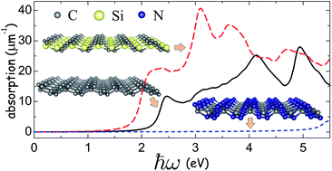
Using density functional theory in combination with the nonequilibrium Green's function formalism we study the electronic transport properties, optical properties and atomic partial charges of the recently proposed isostructural materials: penta-graphene (PG), pentagonal silicon dicarbide (p-SiC2) and pentagonal carbon nitride (p-CN2). Enhanced electronic transport is obtained in p-SiC2 as compared to PG due to the delocalization of the electronic states and smaller variations of the electrostatic potential. This enhancement occurs despite a smaller contribution of Si atoms to the density of states of the system. Penta-SiC2 also displays improved dielectric and optical properties as compared to its all-carbon analogue. For example, larger absorption is obtained in both the visible and the ultraviolet spectral ranges. Strong variation in the atomic partial charge distribution was found in p-SiC2. On the contrary, p-CN2 was not found to exhibit improved optoelectronic properties compared to PG, except for larger partial charges on the surface of the sample. Our findings demonstrate the potential of p-SiC2 in optoelectronic applications.
Recently, Lopez-Bezanilla and Littlewood have proposed another type of 2D material consisting of a pentagonal arrangement of carbon and silicon atoms.17 Density functional theory (DFT) calculations show that the pentagonal silicon dicarbide (p-SiC2) is dynamically stable and exhibits enhanced electronic dispersion when compared to PG. In addition, the band gap of this buckled material can be tuned by applying external strain, possibly increasing the range of applicability of p-SiC2 in optoelectronics. Replacement of the carbon atoms in PG with nitrogen and/or boron atoms can result in the formation of thermally and dynamically stable materials isostructural to PG.18 However, utilization of the full potential of such low-dimensional materials for practical applications requires a fundamental understanding of their structural, electronic, transport and optical properties.
Here, we employ DFT calculations to perform a comparative study of the electronic transport and the optical properties of both PG and p-SiC2. We also study the optoelectronic properties of pentagonal carbon nitride (p-CN2), also recently predicted to be thermally and dynamically stable.18 Atomic partial charge distributions for all systems are calculated. Enhanced electronic transmission was found in p-SiC2 with respect to PG due to the strong delocalization of the electronic states and to more minute variations of the electrostatic potential along the transmission direction. Pentagonal SiC2 also shows improved dielectric and optical properties: the absorption becomes larger for the considered range of the spectrum. The major impact of the Si atoms is also found in the partial charge distribution; this system accumulates almost an order of magnitude more partial static charges on the surface compared to PG. Despite a larger number of partial charges, p-CN2 does not exhibit improved optoelectronic properties compared to PG.
Optical and electronic transport properties were calculated using the nonequilibrium Green's function formalism implemented within the Atomistix toolkit (ATK).27 The electronic structure was calculated self-consistently through DFT/GGA and the electrostatic potentials were determined on a real-space grid with a mesh cut-off energy of 150 Ry. Double-zeta-double-polarized basis sets of local numerical orbitals were employed at each atom. Dielectric and optical properties of the considered systems were obtained by calculating the susceptibility tensors using the Kubo–Greenwood formula:28
![]() | (1) |
α(ω) = Vε0χ(ω). | (2) |
The relation between the refractive index, n, and the complex dielectric constant is given by:
![]() | (3) |
![]() | (4) |
The reflectivity, R, and the loss of function, L, are given by
![]() | (5) |
![]() | (6) |
The lowest energy configuration of p-SiC2 also represents an out-of-plane oscillating pattern in a regular and corrugated manner (Fig. 1(b)). For this system, the middle layer consists of 4-coordinated Si atoms sandwiched between two (top and bottom) layers of 3-coordinated C atoms. As given in Table 1, the system has a larger lattice parameter (b = 4.412 Å) and a larger buckling parameter (δ = 0.66 Å) due to the larger Si–C bond distance, dSi–C = 1.91 Å. The calculated structural parameters of the system are in good agreement with the reports of Lopez-Bezanilla and Littlewood.17 Interestingly, we find strong variations in the partial charge distribution in the system; a large amount of charge is transferred from Si atoms to neighboring C atoms. Consequently, the surface of the material becomes more negatively charged (q(C) = −0.454), whereas the middle plane remains positively charged (q(Si) = 0.908).
b (Å) | δ (Å) | q (middle) | q (top) | ΔEg (PBE) | ΔEg (HSE) | |
---|---|---|---|---|---|---|
PG | 3.639 | 0.608 | 0.132 | −0.066 | 2.270 | 3.250 |
p-SiC2 | 4.412 | 0.660 | 0.908 | −0.454 | 1.429 | 2.395 |
p-CN2 | 3.312 | 0.765 | 0.467 | −0.233 | 4.811 | 6.596 |
The optimized p-CN2 sample has a lattice parameter of b = 3.312 Å and buckling parameter δ = 0.765 Å, which are in good agreement with previous predictions.18 Now, there is a charge transfer from C atoms to N atoms, so that the surface of the systems stays negatively charged. The amount of surface charge is larger than that of PG (see Table 1).
To study the electronic structure properties of the considered systems, we started with calculating the electronic band structures using both non-hybrid (PBE) and hybrid (HSE06) exchange-correlation functionals. PG has a quasi-direct band gap with a PBE value of 2.27 eV, which is in good agreement with the previous reports.6,13 The finite band gap is a consequence of the presence of 4-coordinated sp3-hybridized carbon atoms, which spatially separate the pz orbitals of sp2-hybridized carbon atoms, resulting in electron delocalization.6 The band gap decreases to 1.429 eV in the case of p-SiC2 (see ref. 17 for the detailed discussion of the band gap reduction in the system), whereas the p-CN2 sample shows a significantly larger band gap18 as compared to PG (see Table 1). The HSE band gap of PG is ΔEg = 3.25 eV, which is in good agreement with previous HSE06 reports.6,8 The hybrid exchange-correlation functional also predicts larger band gaps for the other two systems (Table 1). However, the same trend of band gap variation is obtained in HSE06 calculations; p-SiC2 has a smaller band gap as compared to PG, whereas the p-CN2 samples shows the largest band gap.
In order to see the contribution of Si atoms to the DOS of the system, we must examine the projected density of states of p-SiC2. In the case of pristine PG (not shown here), the DOS is dominated by the p-states of the C atoms with smaller contributions from the s-states.6 Interestingly, the conduction band of the p-SiC2 is also determined mainly by the p-states of the C atoms while the contribution from the Si atoms is small. This is shown in Fig. 2, where we plot the projected density of states of the system. The largest contribution of Si atom orbitals to the DOS is obtained only near the valence band maximum, where hybridization of the p-states of Si and C atoms is obtained. The contribution of Si atoms becomes less pronounced deeper inside the valence band. The dominating contribution of carbon atoms at the band edges indicate the importance of structural changes in p-SiC2 rather than the direct electronic contributions from the Si atoms.17 The Fermi level of p-SiC2 is also close to the valence band minimum, as in the case of PG. It has already been shown in ref. 6 that the finite band gap of PG originates from the spatial separation of the pz orbitals of sp2-hybridized atoms on top (bottom) planes. Replacement of these 4-coordinated carbon atoms with Si atoms results in the reduction of the electronic band gap of p-SiC2. The hybrid HSE06 functional also gives qualitatively similar results (see Fig. 2c and d); the conducting band is mainly dominated by the electronic states of the C atoms and the largest contribution from the Si atoms to the DOS is obtained near the valence band maximum.
Fig. 3 shows the DOS of p-CN2 projected on both the C and the N atoms. In this system, both the conduction and the valence bands are mostly dominated by electronic states associated with the N atoms. The contribution of the C atoms are found only within the conduction band, where the hybridization is possible between the p states of the C atoms and p/s states of the N atoms. The hybrid exchange-correlation functional also yielded similar DOS (Fig. 3c and d).
![]() | ||
Fig. 3 Projected density of states of penta-CN2. The results are obtained using PBE (a and b) and HSE06 (c and d) exchange-correlation functional. |
To understand the cause of the increased transmission in p-SiC2 compared to PG, we calculated and compared the projected self-consistent Hamiltonian (PSH) eigenstates of both systems at different energies. As an example, in Fig. 4b–e we show the contour plots of the PSH eigenstates along the middle plane, corresponding to energies indicated in each panel. These eigenstates correspond to states at the valence band maximum (VBM) (b and c) and conduction band minimum (CBM) (d and e). The eigenstate in Fig. 4c represents an extended state, consequently resulting in higher transmission across the sample. On the contrary, the VBM of PG represents a localized state around the C atoms at the top and bottom planes; this localization reduces the probability of an electron crossing the system (see Fig. 4b). Strong localization of the electronic states is also found in the CBM of PG, which reduces the electronic transmission along the c-axis (Fig. 4d). The localization of the electronic states is less pronounced in the CBM of p-SiC2, resulting in larger transmission compared to PG. These findings indicate the importance of electronic localization at the nanoscale for the transport properties in such low dimensional materials.
Another important factor which affects the charge carrier transport is the change in the electrostatic potential profile in the system. Fig. 5 presents the averaged electrostatic difference potential along the transport direction (c-axis) at zero voltage biasing for PG (solid-black curve), p-SiC2 (dashed-red curve) and p-CN2 (dotted-blue curve). Periodic oscillations of the electrostatic potential are obtained for all systems. However, the amplitude of the electrostatic potential oscillations is more than 4 times smaller in p-SiC2 than those of PG. The p-CN2 sample also shows larger potential oscillations compared to p-SiC2. Since the scattering of the charge carriers from these potential oscillations reduces the probability of their transmission, these findings also indicate enhanced electronic transport in p-SiC2 versus the other examined candidates.
![]() | ||
Fig. 5 Electrostatic difference potential along the transport direction for zero potential difference across the samples. |
As a main result, we present in Fig. 6 the real and imaginary parts of the dielectric function as functions of photon energy for PG (solid-black curves), p-SiC2 (dashed-red curves) and p-CN2 (dotted-blue curves). For PG, the static dielectric constant is relatively small ε1(0) = 3.8. This is indicative of the dielectric nature of the material. The first pronounced peak in the ε1(E) is obtained at 2.28 eV, followed by a small peak at 2.92 eV. In the considered range of the spectrum, the last peak is obtained close to the ultraviolet region (4.84 eV). Both qualitative and quantitative changes are obtained in the ε1(E) spectrum of p-SiC2. First, the static dielectric constant increases compared to the case of PG (ε1(0) = 5.3), which may indicate a smaller exciton binding energy in the system. Second, the amplitude of the peaks in the spectrum becomes larger and the positions of the peaks shift to smaller photon energies. The latter is due to the reduced band gap of p-SiC2. Finally, ε1 of p-SiC2 becomes smaller than the one for PG for a particular range of photon energies3,4 eV. Similar changes have been obtained for the imaginary part of the dielectric function, ε2: the value of ε2 becomes larger and the peaks on the ε2(E) curve becomes more pronounced in the case of p-SiC2 in the visible range of the spectrum (see shaded area in Fig. 6b). The p-CN2 samples show the smallest static dielectric function (ε1(0) = 3.2) and no extra features are obtained in the dielectric function for the considered range of the spectrum.
We have also calculated the absorption spectra of each considered system, which are collected in Fig. 7 as a function of the photon energy. In the visible range of spectrum (solid-black curve in Fig. 7), the absorption coefficient of PG shows a maxima at 2.42 eV, followed by a kink at 3.1 eV. Several other peaks are also found in the absorptions spectrum at high photon energies. Significant enhancement in the absorption spectrum is obtained in the case of p-SiC2; the absorption edge becomes smaller due to the reduced electronic band gap and the absorption becomes significantly stronger in both visible and ultraviolet ranges of the spectrum as compared to PG. In addition, the kink at 3.1 eV turns into a pronounced peak followed by a new absorption peak at 3.6 eV. Such improved optical properties of p-SiC2 make this material a promising candidate for photovoltaic applications. The absorption edge shifts to higher energies in the case of p-CN2 due to a larger band gap. Therefore, no absorption is obtained in the visible range of the spectrum (see dotted-blue curve in Fig. 7). The absorption of this candidate is also smaller as compared to the others in the range of ultraviolet photons.
![]() | ||
Fig. 7 Absorption spectra of PG (solid-black curve), penta-SiC2 (dashed-red curve) and penta-CN2 (dotted-blue curve) as a function of photon energy. |
Fig. 8a shows the reflectivity, R, of the considered samples as a function of photon energy. The reflectivity of PG has a maximum at 2.32 eV, after which it decreases with several peaks at different photon energies. In the visible and ultraviolet ranges of the spectrum the reflectivity of PG never exceeds 17%. Larger reflectivity is obtained for the p-SiC2 sample in both the infrared and the visible ranges of the spectrum with two pronounced peaks (Fig. 8a). Both samples show similar reflectivity for the range of photon energies [3.8, 5.8] eV. The reflectivity of p-SiC2 becomes larger again with increasing the photon energy. Strong absorption and larger reflectivity of p-SiC2 in the ultraviolet region (5 eV < E < 10 eV) indicate the potential of this material for anti-ultraviolet ray coating. Finally, Fig. 8b shown the energy-loss spectra of the considered samples as a function of photon energy. The loss spectrum describes the energy loss of fast electrons traversing in the system. Although, the peaks in the loss function corresponds to the minima in the reflectivity spectrum, they are less pronounced for both systems. Interestingly, the p-SiC2 sample shows similar loss function as compared to PG for both visible and ultraviolet range of the spectrum. The p-CN2 sample gives the smallest reflectivity and energy loss in both the visible and the near ultraviolet ranges of the spectrum.
![]() | ||
Fig. 8 Reflectivity (a) and energy-loss spectra (b) as a function of photon energy for PG (solid-black curves), penta-SiC2 (dashed-red curves) and penta-CN2 (dotted-blue curves). |
This journal is © The Royal Society of Chemistry 2016 |