Feng Lianga,
Liang Tiana,
Haijun Zhang*a,
Feng Liangb,
Simin Liub,
Rongsheng Chengb and
Shaowei Zhang*c
aThe State Key Laboratory of Refractories and Metallurgy, Wuhan University of Science and Technology, Wuhan 430081, China. E-mail: zhanghaijun@wust.edu.cn
bSchool of Chemical Engineering and Technology, Wuhan University of Science and Technology, Wuhan 430081, China
cCollege of Engineering, Mathematics and Physical Sciences, University of Exeter, Exeter Ex4 4QF, UK. E-mail: s.zhang@exeter.ac.uk
First published on 28th June 2016
LiSi2N3 nanobelts were synthesized using a novel low temperature molten salt nitridation technique using silicon and melamine as starting materials, and lithium chloride and sodium fluoride to form a reaction medium. The as-synthesized nanobelts were characterized by XRD, FESEM, HRTEM and SAED. The amount of LiSi2N3 increased with temperature. The optimal synthesis temperature for phase pure LiSi2N3 was about 1200 °C, which was about 200 °C lower than that required for the conventional solid-state reaction routes. LiSi2N3 nanobelts about a few hundred nanometers long and 50–200 nm in width were distributed uniformly in the final products. A possible growth mechanism was proposed based on the experimental results. Their photoluminescence emission at 459 nm (2.70 eV) at room temperature suggested that they could be potentially used in light-emitting nano-devices.
Ternary lithium silicon nitrides are one of such interesting materials for luminescent applications.4,5 Several ternary phases including LiSi2N3,6 Li2SiN2,7 Li5SiN3 (ref. 8) and Li8SiN4 (ref. 9) exist in the Li–Si–N ternary system, of which LiSi2N3 with a well-defined wurtzite type structure (space group Cmc21)10 is of particular interest because of its high stability for practical applications. It is generally synthesized via the conventional solid-state reaction route using Li3N and Si3N4 as the starting materials. Unfortunately, this synthesis method suffers from several disadvantages including requirements of high pressure and temperature,6,11,12 and formation of heavily agglomerated LiSi2N3 with large particle size and spheroid morphology, which limits its functional applications.13 To overcome these and to prepare high quality LiSi2N3 nanomaterials with novel morphologies and photoluminescence (PL) properties, an alternative processing route needs to be developed.
In response to this, LiSi2N3 nanobelts have been synthesized for the first time by using a novel low temperature molten salt nitridation (MSN) technique from relatively cheap Si powders and lithium chloride in this work. The effects of reaction temperature on phase composition and morphology of the final products were investigated, and PL properties of as-synthesized LiSi2N3 nanobelts examined.
Phases in product powders were identified by using an X-ray diffractometer (XRD, X'Pert Pro, Philips, Netherlands) with Cu-Kα radiation (λ = 1.5406 Å) operated at 40 kV and 40 mA, with a scanning rate of 2° (2θ) min−1 and a step size of 0.02° (2θ). Morphologies of product phases were examined using a field emission scanning electron microscope (FESEM, Novo 400, FEI Co., USA), a transmission electron microscope (TEM, 2000F, Jeol Ltd., Japan) and selected area electron diffraction (SAED). UV-vis and room-temperature PL spectra were recorded respectively using a UV-vis spectrophotometer (Shimadzu UV-3600, Japan), and a fluorescence spectrophotometer (PerkinElmer LS 55, USA).
Illustrated in Fig. 2a–c are morphologies of samples resultant from 3 h firing at various temperatures in LiCl–NaF. At 1000 °C, many granular LiSi2N3 particles formed on the surface of Si (Fig. 2a). Upon increasing the temperature to 1100 °C, large amounts of nanobelt-like LiSi2N3 phases appeared. On further increasing the temperature to 1200 °C, LiSi2N3 nanobelts with a high aspect ratio of ∼10 were formed (Fig. 2b and c). They were a few hundred nanometers in length and 50–200 nm in width, after epitaxial growth on the surface of Si (Fig. 2c).
The possible growth mechanism of these LiSi2N3 nanobelts can be schematically illustrated in the Fig. 2d and described as follows: in the initial stage, NaF in the LiCl–NaF binary salt diffused onto the Si surface and then reacted to form SiF4(g) according to reaction (1). On the other hand, melamine (C3N3(NH2)3) decomposed in situ to produce NH3 according to reaction (2) (step 1). In addition, LiCl interacted with Si(s), N2(g) and NH3(g), forming eutectic liquid droplets of Li–Si–N via reaction (3) (step 2). Upon oversaturation of the liquid droplets with LiSi2N3, the nucleation of LiSi2N3 would occur, followed by the growth of LiSi2N3 from the droplets (step 3). With increasing the temperature to 1200 °C, more gaseous species (e.g. LiCl, SiF4, and NH3) were generated and dissolved in the droplets, sustaining the growth of LiSi2N3 via reaction (4) (step 4). Owing to the orthorhombic structure nature (i.e., cell parameters a ≠ b ≠ c), the different planes of LiSi2N3 possess different surface energy, and crystal surfaces with lower energies tend to serve as the enclosure surfaces. During the preparation process, the Li, Si and N elements preferred to deposit on the high energy surfaces, finally resulting in simultaneous formation of nanobelt structures. On the basis of the reaction mechanism mentioned above and the observation of LiSi2N3 small particles (Fig. 2a), we proposed that the growth of the as-synthesized LiSi2N3 nanostructures was controlled by the classic VLS mechanism.17
4NaF(l) + Si(s) → SiF4(g) + 4Na(g) | (1) |
2C3N3(NH2)3(s) → 3(CN)2(g) + 4NH3(g) + N2(g) | (2) |
3LiCl(l) + 6Si(s) + 4N2(g) + NH3(g) → 3LiSi2N3(s) + 3HCl(g) | (3) |
LiCl(g) + 2SiF4(g) + 3NH3(g) → LiSi2N3(s) + 8HF(g) + HCl(g) | (4) |
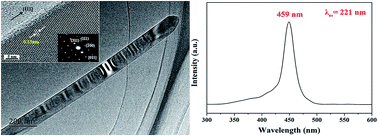
TEM images were further performed along with the SAED patterns to assist identifying the crystalline structure of LiSi2N3 nanobelts resultant from 3 h firing at 1200 °C. Fig. 3a shows a low-magnification TEM image of a representative individual nanobelt, revealing that its aspect ratio was >10 and it had a smooth surface and a uniform width (about 150 nm). Fig. 3b further presents a high-resolution TEM (HRTEM) image of its edge area, showing that the interplaner distance was 0.33 nm which matched with the (111) plane of LiSi2N3. This result indicated that the LiSi2N3 nanobelt grew along the [111] direction, as suggested by the XRD results (Fig. 1). Moreover, the SAED pattern (inset in Fig. 3b) confirmed that the LiSi2N3 nanobelt was single crystalline in nature.
The UV-vis absorption spectrum of as-synthesized LiSi2N3 nanobelts (Fig. 4a) shows nearly zero absorbance in the visible range but significant absorbance in the UV region. A narrow absorption peak centered at 221 nm appeared, which corresponded to a band gap of ∼5.61 eV. This value was smaller than that (at ∼6.40 eV) reported previously for bulk LiSi2N3.4 Such a shift in the present sample could be attributed to the saddle point transition in the band structure.18 The optical band gap (OBG) estimated19 from the UV-vis absorption spectrum of as-synthesized LiSi2N3 nanobelts was ∼5.25 eV (see the inset in Fig. 4a). To further understand optoelectronic properties of as-synthesized LiSi2N3 nanobelts, their PL properties were also examined. Ultraviolet light used to excite the nanobelts was obtained from xenon lamp and its excitation wavelength was set at 221 nm. As seen from the room-temperature PL emission spectrum (Fig. 4b), intense luminescence in the violet-blue spectral range from 350 to 500 nm, with a main emission peak at around 459 nm (2.70 eV), occurred. Similar phenomena were also observed for BN nanoplates and AlN nanoneedles,20,21 which are believed to arise from the surface effect (increased surface-to-volume ratios) and defect concentrations. Such explanation could also be used for present observed optical behavior of the as-synthesized LiSi2N3 nanobelts. However, detailed mechanisms on the PL properties of the LiSi2N3 nanobelts are not fully understood and require more systematic investigation. The intensive PL emission spectrum indicated that LiSi2N3 nanobelts prepared in this work could be potentially used in optical and optoelectronic devices such as LEDs, blue-light source, and UV detector.
![]() | ||
Fig. 4 (a) UV-vis absorption spectrum and optical band gap analysis (inset), and (b) emission photoluminescence (PL) spectrum (λex = 221 nm) of as-synthesized LiSi2N3 nanobelts. |
This journal is © The Royal Society of Chemistry 2016 |