
Cl2/Ar based dry etching of GaCrN using inductively coupled plasma
Tarkeshwar C. Patil
Department of Electrical Engineering, IIT Bombay, Powai, Mumbai – 400076, India. E-mail: tarkeshwarcpatil@gmail.com
First published on 14th July 2016
Abstract
Dry etching of a novel spintronic material, Ga1−xCrxN (where 0.01 < x < 0.07) using ICPRIE is reported for the first time. The etch rate is compared with that of GaN. It is observed that for various gas flow rates and process conditions, etch rates change significantly due to the presence of Cr. While the physical component of dry etching does not change much compared to that of GaN, the chemical component plays a significant role in the enhanced etch rates. The change may be attributed to the presence of new etch products for GaCrN. It is observed that the etch rate decreases with increasing x. The potential etch mechanism is also discussed. It is also observed that increasing the value of x leads to higher surface roughness which is verified using AFM. The main role in making the etched surface rough is attributed to the presence of non-volatile byproducts formed during the etching of GaCrN.
1. Introduction
Recently group III nitrides have attracted much attention because of their wide spectrum of potential applications in semiconductor electronics ranging from optoelectronic devices for the blue ultraviolet spectral region to high speed systems in the form of high electron mobility transistors (HEMTs), and other forms of transistors; high power applications by providing a basic building block of power devices etc.The key aspects pertaining to plasma etching are etch-rate, etch surface properties, selectivity, and anisotropy. High etch rates are observed in high-density plasma techniques.1–5 However, plasma etching as a process step for device fabrication must be optimized for the aforementioned aspects. Increased contact resistance and surface-related carrier recombination observed in the device operation are associated to the etching-induced surface roughness.6–8 Regardless of this key issue, there are very few reports which focus on etching-induced surface properties of the III nitrides.9–11
A lot of research has been carried out to study dry etching of GaN based materials, particularly GaN, AlGaN and InGaN,12–14 which is very essential for nanoelectronic device fabrication. Due to the strong bond strength of gallium to nitrogen achieving good etching characteristics in GaN is a challenge. Numerous methods have been employed for the etching of GaN and its related compounds, which include dry etching utilizing high density plasmas and conventional reactive ion etching. Due to chemically stable nature and insolubility in most common etchants of GaN wet chemical etching shows isotropic etching profiles and slower etching rates than the dry etching technique.15 Many investigations involving dry etching of GaN and related compounds in various chemistries have applied three conventional dry etching techniques: reactive ion etching (RIE), electron cyclotron resonance plasma etching (ECR), and inductively coupled plasma etching (ICP).1,16,17 Low etching rates, less anisotropic etching profile, and more surface damage are characteristic of RIE process. These characteristics are attributed to the low plasma densities and higher process pressures. In general, the etching rates of RIE increase with an increasing direct current (DC) bias. Such a phenomenon is owing to the acceleration of energetic ions from the plasma to sample. However, the high energy ion bombardment of the surface damages the sample. Therefore, attempts to minimize the damage by reducing the ion energy or increasing the chemical activity in the plasma usually decrease the etching rate or lead to less anisotropy. Owing to the higher plasma density of ECR than RIE, a previous study has demonstrated that using ECR plasma etching yields much faster etching rates and higher degree of anisotropy than RIE etching for III nitrides.18 In addition, low pressure operation of ECR tends to damage the material to a lesser extent than RIE etching owing to a lower ion energy. ICP offers an alternative high-density plasma technique to etch III nitrides.2,19 As widely acknowledged, the ICP source is easier to scale up than ECR and has the merits of relatively low cost and availability of truly automatic matching networks for tuning of the plasma discharge.
In this work it is reported that GaCrN can be a very useful material for spintronic devices and it can be used as a ferromagnetic spin injector and detector. So far there is no report on etching induced surface properties of GaCrN. Thus, for the first time, dry etching of this novel material by ICP RIE is reported. The etch mechanism is analyzed and its comparison of the etch rate with that of GaN along with its effect on the surface morphology of both GaN as well as GaCrN is looked upon.
2. Experiment
The GaN samples are grown on c-plane sapphire substrate by hydride vapor phase epitaxy (HVPE). The organic cleaning of the sample with size 1 cm × 1 cm is done with tri-chloroethylene (TCE) followed by acetone. The samples are then cleaned in methanol for five minutes. A thin layer of Cr (15 nm) is then deposited by using e-beam evaporation technique. The sample is annealed at 800 °C for 35, 40, 55, 75 and 80 cycles of 1 min each using rapid thermal annealing (RTA). Cr thermally diffuses into GaN to form GaCrN. The residual Cr is etched away from the top surface by using a standard Cr etchant. The samples are then patterned using optical lithography using a HEMT MESA mask used to fabricate India's first GaN HEMT by the author20,21 and loaded into ICPRIE tool, Sentech Germany model SI 500 along with the undoped GaN sample. The etch depths are measured using surface profilometry and scanning electron microscopy (SEM). The surface roughness in the etched area of the samples are examined using atomic force microscopy (AFM). In order to study the ferromagnetism in GaCrN, temperature dependent hysteresis measurements using a superconducting-quantum-interference-device (SQUID) magnetometry is carried out. To investigate the structural and elemental composition cross-sectional high resolution transmission electron microscopy (HR-TEM), energy-dispersive X-ray spectroscopy (EDX), X-ray fluorescence (XRF), X-ray diffraction (XRD) have been carried out.3. Results and discussion
Energy-dispersive X-ray spectroscopy (EDX) is used to find the composition of the GaCrN alloy. It is observed that Cr is almost uniformly distributed at ∼1–7% through the GaN layer as the number of annealing cycles are increased from 35 to 80. Fig. 1a shows the cross-sectional SEM image for spectrum 3 of EDX analysis at 123 nm below the surface for sample with 40 cycles. EDX composition at different locations spectrum 1 to spectrum 8 with an increase in the depth of the cross section of the sample annealed for 40 cycles is listed in Table 1. Spectrum 3 is at 123 nm from the surface above which no Cr is detected. Table 2 list the elemental compositions obtained for 80 cycles samples. Fig. 1b shows the spectrums for various elements found in the 80 cycles sample along with the cross-sectional SEM view showing the depth profile. Cr concentration profile shows that Cr is uniformly diffused through the entire GaN thin-film and no apparent cluster formation is observed with a segregation at the GaN/sapphire interface. Fig. 1c shows the graphical representation of elemental analysis from EDX spectroscopy, which confirms that there are no ferromagnetic impurities in the GaCrN sample. | ||
| Fig. 1 EDX analysis of GaCrN samples (a) SEM image of spectrum 3 analyzed at 123 nm below the surface for 40 cycles annealed GaCrN sample, (b) analysis for 80 cycles annealed GaCrN sample showing uniform diffusion of Cr through the GaN layer and segregation near GaN/Al2O3 interface and (c) graphical representation of species composition in 80 cycles annealed GaCrN sample which confirms absence of any ferromagnetic species present in the sample. | ||
| Spectrum | N | O | Al | Ti | Cr | Ga |
|---|---|---|---|---|---|---|
| a All results in atomic%. | ||||||
| Spectrum 1 | 31.53 | 6.40 | 2.09 | 1.00 | 58.98 | |
| Spectrum 2 | 0.00 | 36.69 | 1.94 | 2.23 | 0.80 | 58.33 |
| Spectrum 3 | 0.00 | 39.46 | 3.06 | 1.84 | 0.51 | 55.14 |
| Spectrum 4 | 32.66 | 1.91 | 1.98 | 63.45 | ||
| Spectrum 5 | 38.24 | 61.76 | ||||
| Spectrum 6 | 43.36 | 56.64 | ||||
| Spectrum 7 | 0.00 | 25.65 | 1.47 | 1.08 | 71.80 | |
| Spectrum 8 | 38.24 | 61.76 | ||||
| Max. | 43.36 | 39.46 | 6.40 | 2.23 | 1.00 | 71.80 |
| Min. | 0.00 | 25.65 | 1.47 | 1.08 | 0.51 | 55.14 |
| Spectrum | N | O | Si | Cr | Ga |
|---|---|---|---|---|---|
| a All results in atomic%. | |||||
| Spectrum 1 | 53.80 | 3.61 | 0.94 | 7.81 | 33.08 |
| Spectrum 2 | 53.59 | 10.72 | 35.68 | ||
| Max. | 53.80 | 17.20 | 0.94 | 10.72 | 35.68 |
| Min. | 36.25 | 3.61 | 0.94 | 7.81 | 31.40 |
XRF analysis for 55 cycles GaCrN sample also shows 2.6291![[thin space (1/6-em)]](https://www.rsc.org/images/entities/char_2009.gif) :97.3709 Cr:Ga ratio as tabulated in Table 3 and corresponding graphical representation is presented in Fig. 2a. The structural analysis was carried out using XRD measurement. Fig. 2b shows the XRD analysis of GaN sample with the respective peaks for GaN and Al2O3 (sapphire). Fig. 2c shows the XRD analysis of GaCrN samples (35, 40, 55, 75, and 80 cycles) with the respective peaks for GaCrN and Al2O3 (sapphire). These XRD results for GaCrN are in well accordance with.22 On comparing both the XRD plots for diffraction angle 2θ range of 34° to 35°, it is observed that there is a minor shift for GaCrN to the right because of the larger Cr atom substituting Ga atom as seen in Fig. 2d.
:97.3709 Cr:Ga ratio as tabulated in Table 3 and corresponding graphical representation is presented in Fig. 2a. The structural analysis was carried out using XRD measurement. Fig. 2b shows the XRD analysis of GaN sample with the respective peaks for GaN and Al2O3 (sapphire). Fig. 2c shows the XRD analysis of GaCrN samples (35, 40, 55, 75, and 80 cycles) with the respective peaks for GaCrN and Al2O3 (sapphire). These XRD results for GaCrN are in well accordance with.22 On comparing both the XRD plots for diffraction angle 2θ range of 34° to 35°, it is observed that there is a minor shift for GaCrN to the right because of the larger Cr atom substituting Ga atom as seen in Fig. 2d.
| Element | Line type | Energy | ms% | mol% | K | Net | Error% |
|---|---|---|---|---|---|---|---|
| Cr | K | 5.41 | 2.6291 | 3.4940 | 0.0140970 | 2282 | 1.8691 |
| Ga | K | 9.24 | 97.3709 | 96.5060 | 0.3769092 | 68148 |
3.2807 |
 | ||
| Fig. 2 (a) XRF analysis for 80 cycles annealed GaCrN sample showing the elemental composition for Ga and Cr species, (b) XRD data for GaN sample, (c) XRD data for 35, 40, 55, 75 and 80 cycles annealed GaCrN samples and (d) comparative study of XRD data for GaN and GaCrN showing a minor right shift in peak position for the diffraction angel 2θ in the range of 34° to 35°. | ||
HRTEM was performed at various spots across the cross-section of the 80 cycles GaCrN sample to investigate the origin of ferromagnetism. A single diffraction pattern for GaCrN, viz. that of GaN, and GaN crystal lattice planes were observed showing no microscopic or macroscopic level secondary phases (Fig. 3a and b) which were confirmed from selected area electron diffraction (SAED) pattern shown as an inset to Fig. 3b. This ensures that Cr does not form clusters in GaN. Hysteresis measurements are performed to ensure ferromagnetic behavior in these samples. Fig. 3c shows the hysteresis (M–H) curve at 300 K and the inset shows M–H curve at 5 K as obtained from superconducting quantum interference device (SQUID) magnetometer. The hysteretic behavior confirms the ferromagnetic nature of this material. The coercive field is found to decrease from 450 Oe at 5 K to 270 Oe at 300 K. Magnetic property of the Cr-doped sample is examined using a SQUID magnetometer. Control samples with the residual Cr and bare GaN wafers were also analyzed using SQUID measurement. Diamagnetic behavior is exhibited by the samples with residual Cr-layer after the thermal drive-in diffusion whereas a paramagnetic nature of hysteresis curve is seen in the bare n-GaN sample at high magnetic field. This further corroborates that the ferromagnetic property of the GaCrN sample is due to Cr doping of GaN.
 | ||
| Fig. 3 (a) Cross-sectional HRTEM image for 80 cycles annealed GaCrN sample (b) cross-sectional HRTEM image for 80 cycles annealed GaCrN sample at different location on the sample, inset shows a SAED pattern showing no secondary phase formation in GaCrN, (c) M–H curve depicting the presence of ferromagnetism in GaCrN at 300 K, inset shows M–H curve at 5 K it is observed that the coercive field is found to decrease from 450 Oe at 5 K to 270 Oe at 300 K. | ||
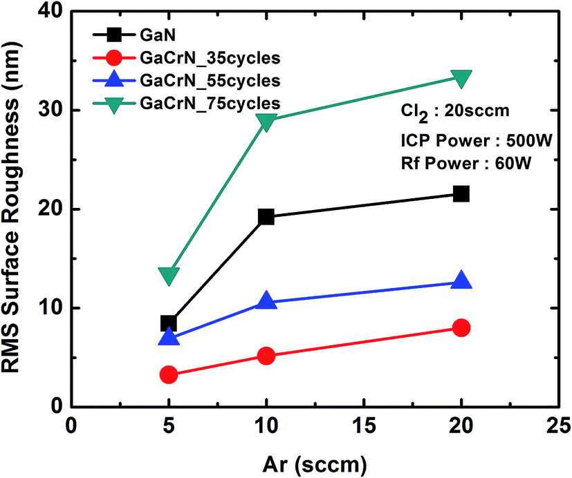
The samples were etched for various gas flow rates and process conditions. Table 4 lists the process parameters for different recipes used in this research work. Fig. 4 shows etch-rates of GaN and 35, 55, 75 cycles annealed GaCrN samples as a function Ar flow rate. It is seen that upto ∼1% of Cr content in GaCrN, the bond strength becomes weak and thus we get much higher etch rates. Likewise, we can see that as the Cr percentage increases the relative selectivity of GaCrN to GaN decreases, that signifies the bond strength of GaCrN when annealed for 75 cycles becomes stronger than that of GaN. While the GaN etching process produces volatile chemical by-products such as GaCl3 as shown in chemical reaction 1, the etching seizes progress without sufficient energetic ion bombardment because of the high bond strength of the material as can be seen in Fig. 5.23,24 It may be noted that the etch rate is maximum when the Cl2 flow rate is double that of Ar. This not only due to the large concentration of Cl free radical species, but also efficient sputter desorption of the subsequent etch products. When both of these gases are in equal amounts, the etch rate falls drastically. This is expected as the Ar species in the plasma start removing the Cl free radicals much before their lifetime. The effective lifetime of Cl radicals and hence the time within which they can form volatile etch products such as GaCl3 is reduced. Fig. 4 also indicates that the etch rate reduces significantly as the Ar flow rate is reduced. This is in agreement with the previous discussion that minimizing the Ar flow rate would result in poor sputter desorption of the etch products and subsequently a lesser etch rate.
 | (1) |
 | (2) |
| Parameter | Recipe-I | Recipe-II | Recipe-III |
| Chamber pressure | 0.67 Pa | 0.67 Pa | 0.67 Pa |
| Cl2:Ar |
20:5 sccm |
20:10 sccm |
20:20 sccm |
| ICP power | 500 W | 500 W | 500 W |
| Rf power | 60 W | 60 W | 60 W |
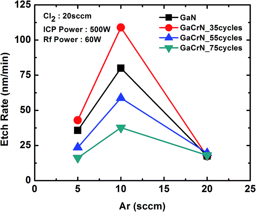 | ||
| Fig. 4 Variation in etch-rates of GaN and 35, 55, 75 cycles annealed GaCrN samples as a function of Ar flow rate. | ||
 | ||
| Fig. 5 The RMS roughness of GaN and 35, 55, 75 cycles annealed GaCrN samples as a function of Ar flow rate. | ||
The etching of GaCrN produces volatile chemical by-products such as GaCl3, CrCl2 and very unstable CrCl4 and non-volatile CrCl3 as shown in chemical reaction (2). However, the etch rate is higher compared to that of GaN. The degree of enhancement depends on the Ar flow rate. It may be noted that under the same process condition (Recipe-II) GaCrN (35 cycles) sample exhibits a higher etch rate of 109 nm min−1 when the Cl gas flow rate is doubled that of Ar. This may be attributed to an etch product of Cr, that has a higher tendency to form a halide based compound compared to Ga which forms GaCl3. This is confirmed in Recipe-I where the physical (Ar) component is reduced and the etch rate comes down for all the samples. However, the etch rate for GaCrN (35 cycles) is still more than that of the other samples. This indicates that the etch by-products in case of GaCrN samples are different compared to the that of GaN as mentioned in chemical reaction (2). In Recipe-III all the samples are in the surface reaction rate limited regime as Ar removes the Cl free radicals much ahead of their lifetime. Hence, both the samples show the same etch rate. This also confirms that the chemical component is the dominant part in etching GaCrN.
In Fig. 5, the RMS surface roughness are shown for the samples after etching, which signifies the surface damage post dry etching. Since surface quality plays an important role in device performance, especially at low temperatures.
Here it is observed that the RMS roughness goes on increasing as the Cr concentration in GaCrN increases. GaCrN sample annealed for 35 cycles, shows the minimum RMS roughness, which means that addition of ∼1% of Cr to GaN makes the surface smoother than that of GaN because the unstable chromium(II) chloride, which is formed as a by-product during the etching forms a very thin layer on the surface, thus protecting the surface from becoming rougher. Whereas for the GaCrN annealed for 75 cycles, shows the maximum RMS roughness because of the formation of the halides of chromium, which are usually solid in nature and tend to get deposited in the form of clusters on the etched surface itself. Also, in each case, it can be seen that as the Ar percentage increases, i.e. increase in the physical component, the RMS roughness also increases.25
This is also depicted in the AFM surface morphology in Fig. 6 with its roughness analysis for GaN and GaCrN (35, 55 and 75 cycles) samples etched using Recipe-II. AFM images show the surface characteristics for GaN and GaCrN samples, here it is observed that the surface becomes more rough for the 75 cycle sample as compared to that of GaN and 35 cycle GaCrN. Thus the surface damage observed confirms the presence of formation of the halides of chromium.
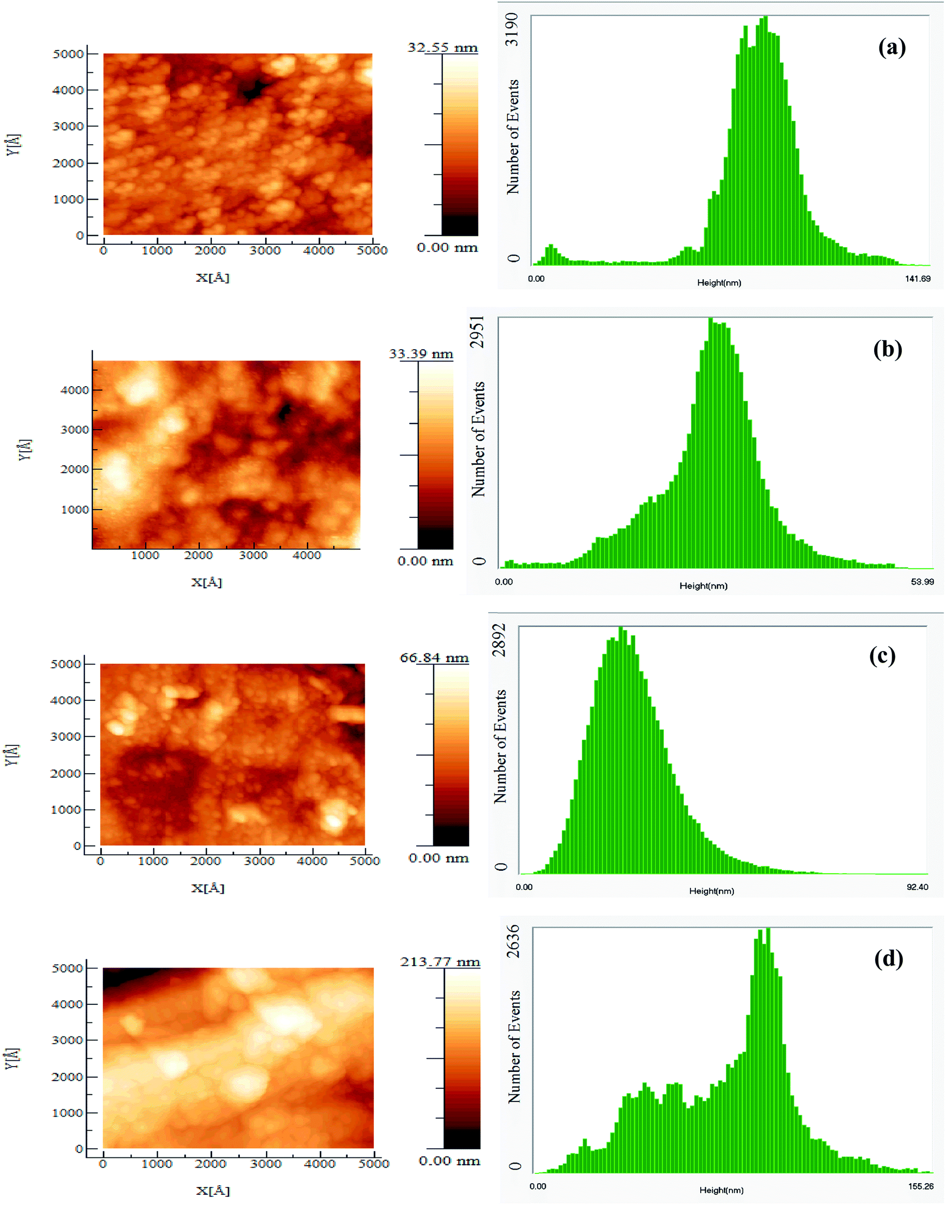 | ||
| Fig. 6 AFM surface morphology of (a) GaN, GaCrN [(b) 35, (c) 55 and (d) 75 cycles] samples etched using Recipe-II with their respective surface analysis. | ||
SEM image of the step profile, post etching is shown in Fig. 7a and b for 55 and 75 cycles annealed GaCrN sample respectively.
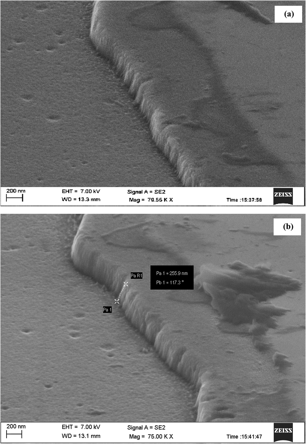 | ||
| Fig. 7 Cross-sectional SEM image depicting the step profile of etched GaCrN (a) 55 cycles and (b) 75 cycles samples. | ||
4. Summary
In this study, the effects of percentage gas addition of Ar to Cl2 on the GaN and Ga1−xCrxN etch characteristics were investigated using ICPRIE. It is found that there is an enhancement in the etch rate when x ≊ 0:01 and the etched surface becoming smoother. But as x increases, there is a sharp decrease in the etch rate due to increases in the bond strength of GaCrN and it is also seen that the etched surface becomes rough, mainly due to the presence of non-volatile halides of Cr getting deposited over the surface. Further, it is confirmed that the chemical component plays the dominant role in dry etching. Presence of Cr leads to additional by-products in addition to that produced by GaN. The ferromagnetism behavior of GaCrN and its elemental as well as structural composition is also studied confirming room temperature ferromagnetism with better crystallinity without any cluster formation and presence of Cr is being attributed towards the observation of ferromagnetism in GaCrN.
Acknowledgements
Indian Institute of Technology, Bombay is being acknowledged for providing the necessary facilities to carry out the reported work.References
- R. J. Shul, G. B. McClellan, S. A. Casalnuovo, D. J. Rieger, S. J. Pearton, C. Constantine, C. Barratt, R. F. Karlicek Jr, C. Tarn and M. Schurman, Appl. Phys. Lett., 1996, 69, 1119 CrossRef CAS.
- S. A. Smith, C. A. Wolden, M. D. Bbremser, A. D. Hanser, R. F. Davis and W. V. Lampert, Appl. Phys. Lett., 1997, 71, 3631 CrossRef CAS.
- Y. H. Lee, H. S. Kim, J. Y. Yeom, J. W. Lee, M. C. Yoo and T. I. Kim, J. Vac. Sci. Technol., A, 1998, 16, 1478 CAS.
- C. B. Vartuli, S. J. Pearton, J. W. Lee, J. Hong, J. D. Mackenzie, C. R. Abernathy and R. J. Shul, Appl. Phys. Lett., 1996, 69, 1426 CrossRef CAS.
- K. Zhu, V. Kuryatkov, B. Borisov, G. Kipshidze, S. A. Nikishin, H. Temkin and M. Holtz, Appl. Phys. Lett., 2002, 81, 4688 CrossRef CAS.
- D. A. Francis, C. J. Chang-Hasnain and K. Eason, Appl. Phys. Lett., 1996, 68, 1598 CrossRef CAS.
- M. V. Bazylenko, M. Gross and M. Faith, Appl. Phys. Lett., 1996, 69, 2178 CrossRef CAS.
- B. Rong, E. V. D. Drift, R. J. Reeves, W. G. Sloof and R. Cheung, J. Vac. Sci. Technol., B: Microelectron. Nanometer Struct.–Process., Meas., Phenom., 2001, 19, 2917 CrossRef CAS.
- J. W. Lee, J. Hong, C. R. Abernathy, E. S. Lambers, S. J. Pearton, W. S. Hobson and F. Ren, J. Vac. Sci. Technol., B: Microelectron. Nanometer Struct.–Process., Meas., Phenom., 1996, 14, 2567 CrossRef CAS.
- Y. B. Hahn, R. J. Choi, J. H. Hong, H. J. Park, C. S. Choi and H. J. Lee, J. Appl. Phys., 2002, 92, 1189 CrossRef CAS.
- S. Tripathy, A. Ramam, S. J. Chua, J. S. Pan and A. Huan, J. Vac. Sci. Technol., A, 2001, 19, 2522 CAS.
- S. Rosli, A. Aziz and M. Hashim, Sains Malays., 2001, 40(1), 79–82 Search PubMed.
- Ji-M. Lee, Ki-M. Chang, In-H. Lee and S.-J. Park, J. Electrochem. Soc., 2000, 147(5), 1859–1863 CrossRef.
- W. U. Tong, Z.-B. Hao, G. Tang and Y. Luo, Jpn. J. Appl. Phys., 2003, 42, L257–L259 CrossRef.
- R. F. Davis, Proc. IEEE, 1991, 79, 702 CrossRef CAS.
- M. E. Lin, Z. F. Fan, Z. Ma, L. H. Allen and H. Morkoc, Appl. Phys. Lett., 1994, 64, 887 CrossRef CAS.
- R. J. Shul, S. P. Kilcoyne, M. Hagerott Crawford, J. E. Parmeter, C. B. Vartuli, C. R. Abernathy and S. J. Pearton, Appl. Phys. Lett., 1995, 66, 1761 CrossRef CAS.
- C. B. Vartuli, J. D. Mackenzie, J. W. Lee, C. R. Abernathy, S. J. Pearton and R. J. Shul, J. Appl. Phys., 1996, 80, 3705 CrossRef CAS.
- R. J. Shul, G. B. McClellan, S. J. Pearton, C. R. Abernathy, C. Constantine and C. Barratt, Electron. Lett., 1996, 32, 1408 CrossRef CAS.
- S. Subramanian, T. Patil, A. Mukherjee, A. Ghosh and P. Mahajan, 2009, DELIVERABLE# 4: GaN Devices. CEN, IIT Bombay, Mumbai, India, retrieved from https://www.ee.iitb.ac.in/%7Etarkeshwar/deliverable_4.pdf.
- CEN Brochure, CEN IIT Bombay, Mumbai, India, page 7, retrieved from http://www.cen.iitb.ac.in/cen/about-us/pdf/cen_brochure.pdf.
- M. Hashimoto, Y. K. Zhou, M. Kanamura, H. Katayama-Yoshida and H. Asahi, J. Cryst. Growth, 2003, 251, 327–330 CrossRef CAS.
- Y. Han, S. Xue, W. Guo, Y. Luoa, Z. Hao and C. Sun, Jpn. J. Appl. Phys., 2003, 42, L1139–L1141 CrossRef CAS.
- Y. Han, S. Xue, W. Guo, Y. Luoa, Z. Hao and C. Sun, Jpn. J. Appl. Phys., 2003, 42, L1139–L1141 CrossRef CAS.
- J. Mathew, R. M. Mohanty, R. Sundaresan, V. Sivan and K. Balasubramanian, Fusion Eng. Des., 2010, 85, 824–827 CrossRef CAS.
| This journal is © The Royal Society of Chemistry 2016 |