
 Open Access Article
 This Open Access Article is licensed under a
 Creative Commons Attribution 3.0 Unported Licence
Disposable (bio)chemical integrated optical waveguide sensors implemented on roll-to-roll produced platforms
Sanna
Aikio
*a,
Martin
Zeilinger
b,
Jussi
Hiltunen
a,
Leena
Hakalahti
a,
Johanna
Hiitola-Keinänen
a,
Marianne
Hiltunen
a,
Ville
Kontturi
c,
Samuli
Siitonen
c,
Jarkko
Puustinen
d,
Peter
Lieberzeit
b and
Pentti
Karioja
a
aVTT Technical Research Centre of Finland, Kaitoväylä 1, FI-90590, Oulu, Finland. E-mail: sanna.aikio@vtt.fi
bUniversity of Vienna, Faculty for Chemistry, Department of Analytical Chemistry, Währinger Straße 38, 1010 Vienna, Austria
cNanocomp Oy Ltd, Ensolantie 6, FI-80710 Lehmo, Finland
dUniversity of Oulu, Faculty of Information Technology and Electrical Engineering, Department of Electrical Engineering, Microelectronics and Materials Physics Laboratories, Pentti Kaiteran katu 1, FI-90014 Oulu, Finland
First published on 17th May 2016
Abstract
To enable wide spread dissemination of sensors in cost-critical applications and resource poor settings, methods to implement sensor chips using low-cost materials and mass-manufacturing methods are developed. In this paper we demonstrate that disposable polymeric integrated Young interferometer (YI) sensor chips, implemented on roll-to-roll mass-manufactured waveguides, are applicable for analyte specific sensing of small molecules and for multi-analyte detection of biomolecules. For the chemical sensing of small molecules, a sensor chip was functionalized with a molecularly imprinted polymer (MIP). We demonstrate that the MIP receptor layer is compatible with a polymer-based evanescent wave sensor for direct refractive index sensing. For multi-analyte detection of biomolecules, antibody-based receptor layers were patterned by inkjet printing onto the sensor surface demonstrating the applicability of the method with integrated YI chips. Demonstration of the analyte specific chemical- and biosensing with disposable polymeric YI sensor chips opens new possibilities to implement low-cost (bio)chemical sensors.
Introduction
Research on micro total analysis and optofluidic systems is advancing rapidly, developing sensor technologies for a wide range of applications including point-of-care diagnostics, environmental monitoring and food safety.1,2 To enable wide spread dissemination of the sensors, also in resource poor settings, there is a need for sensor chips that are sensitive, robust, and reliable, and that can be implemented using low-cost fabrication methods and materials.Waveguide based integrated interferometric sensors, such as integrated Young interferometers (YIs), show potential for low-cost sensor applications.3 Integrated YI sensors utilize the evanescent wave field of the guided optical wave to directly sense the refractive index (RI) changes at or within a few hundred nanometres of the waveguide surface. The label-free sensing method enables simpler sample handling, and reduced complexity and cost of the sensor chip.3 YI sensor chips are reported to detect RI differences 10−5 to 10−8 refractive index units (RIU) showing some of the lowest limit of detection values among integrated interferometric sensors.3–6
The fabrication of YI sensor chips has relied on batch-based manufacturing methods,3 for example micromachining of silicon wafers, using inorganic4,5,7–10 or low-cost polymeric6,11–13 materials. Recently, the authors have demonstrated that single-mode waveguides for polymeric integrated YI sensor chips can be fabricated on flexible foils with length of hundreds of meters by using continuous ultra-high volume roll-to-roll (R2R) manufacturing methods making the chips inherently disposable.14 Quality of the waveguides was assessed by measuring the attenuation properties of hundreds of samples showing that waveguides with repeatable performance were manufactured. It was also demonstrated that the unfunctionalized integrated YI sensor chips were capable to detect ambient unspecific RI changes in the level of 10−6 RIU and quantify them in the level of 10−5 RIU by using aqueous glucose solutions, showing thus rather comparable performance than reported earlier for polymeric YI sensors.6,13
For analyte specific sensing, YI sensor chips need to be functionalized with a receptor layer that binds analyte molecules selectively to the sensor surface. When analyte molecule binds to a receptor it replaces sample matrix that typically has lower RI, and induces a RI change. The magnitude of the RI change depends on the RIs of the chosen analyte molecule and sample matrix. Of biological receptors, antibodies have been used to functionalize inorganic and polymeric YI sensors for detection of proteins and viruses including demonstration of multi-analyte sensing.6,8,9,15,16 Artificial receptor layers, such as molecularly imprinted polymers (MIPs), provide another route for sensor functionalization. MIP receptor layers may be advantageous for low-cost sensors due to their potential to be low-cost, robust, repeatable, and mass-manufacturable.17 MIP receptor layers have been applied with silicon-based interferometric sensor chips to detect vapor phase trinitrotoluene and proteins.18,19 In this work we study the applicability of MIP receptor layer with polymeric YI sensor chips.
The antibody receptor layers of integrated YI sensors are applied by either incubating antibody solution on the chip surface,9 or by flowing the antibody solution through the flow-cell assembled on top of the sensor chip enabling the binding of the antibodies onto the sensor surface.6,8,15,16 The MIP receptor layers are formed by either dip coating the YI sensor chip18 or injecting the polymer solution onto the sensor surface, and performing the polymerization under glass plate resulting in a thin receptor layer.19 Patterned functionalization by inkjet printing of antibodies has been demonstrated for multi-analyte functionalization of silicon-based ring resonator sensors,20 however that method has not been utilized to functionalize YI sensor chips. Functionalization by inkjet printing is especially interesting for low-cost sensors since, as an additive method, it minimizes the consumption of potentially expensive receptor materials, and is also considered to be compatible with mass-production methods.21
In this paper, we demonstrate the applicability of the disposable polymeric multi-analyte YI sensor chips having R2R fabricated waveguides for analyte specific chemical- and biochemical sensing. Due to strict surface quality requirements of optical waveguides, it is not self-evident that receptor layers can be applied onto polymeric waveguides without deteriorating their capability to guide light and act as a sensor, for example due to increased scattering. We use melamine as a model analyte to demonstrate the chemical sensing of small molecules and the applicability of the MIP receptor layer with a polymeric evanescent wave sensor chip for direct RI sensing. The multi-analyte sensor design and patterning of the MIP and the reference non-imprinted polymer (NIP) layer onto a single sensor chip enables the simultaneous measurement of the analyte specific binding into the MIP layer and the non-specific sample matrix effects. The multi-analyte detection of biomolecules is demonstrated by using C-reactive protein (CRP) and human chorionic gonadotropin (hCG) as model analytes. We also demonstrate the applicability of the inkjet printed antibody-based receptor and reference layers with integrated YI sensor chips for multi-analyte detection. The chosen functionalization schema enables real-time detection of the specific binding of analytes and suppression of non-specific sample matrix effects.
Sensor chip embodiments and sensing principle
Illustration of the sensor chip is shown in Fig. 1(a). Sensor chip has an input waveguide that branches into four waveguides forming two parallel Young interferometers, named YI1 and YI2, integrated into one sensor chip. Both of the interferometers contain a reference and a measurement waveguide. The separation between the reference and measurement waveguides is increased at the sensing area enabling patterning of the measurement windows and receptor layers with loose positional tolerances. Measurement window is an opening in the passivating overcladding layer of the waveguides enabling the interaction of the sample with the evanescent wave field of the light propagating in the underlying waveguide.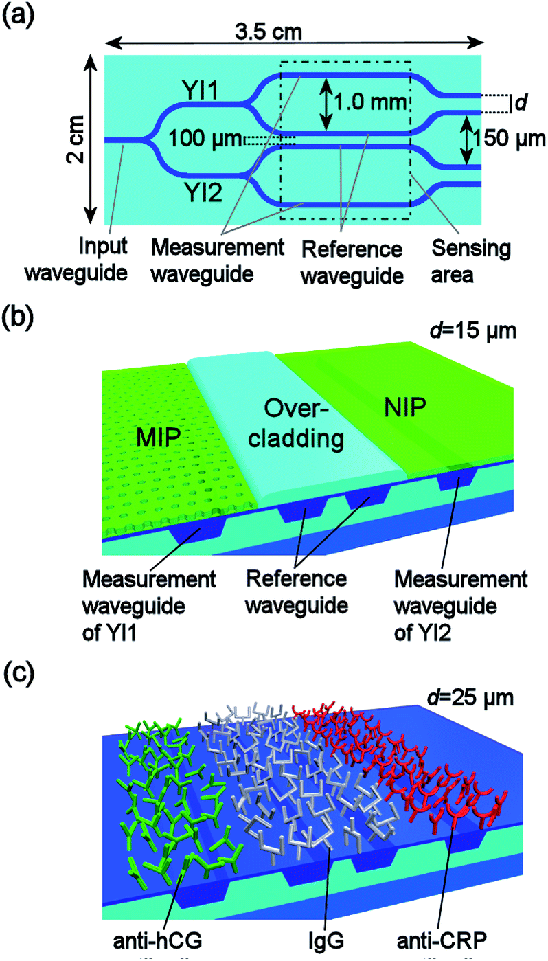 | ||
| Fig. 1 (a) Top view illustration of the sensor chip with names of the parts and dimensions. (b) Illustration of the cross-cut structure of the MIP functionalized sensor chip within the sensing area showing the MIP and NIP coatings on the respective measurement waveguides, and the passivating overcladding layer on the reference waveguides. (c) Antibody functionalized chip having analyte specific anti-hCG and anti-CRP antibody coatings on the respective measurement waveguides and reference IgG coating on the reference waveguides. The separations of the measurement and the reference waveguides at the outcoupling end of the chip, d, are shown next to the sensor illustrations in (b) and (c). | ||
Illustration of the cross-section of the sensor chip structure for the chemical sensing within the sensing area is shown in Fig. 1(b). The reference waveguides of both YIs were passivated by the overcladding layer and were thus not exposed to sample solutions. The measurement windows were formed by leaving a length of 10 mm of the measurement waveguides without the overcladding layer. The MIP receptor layer was applied into the measurement window of YI1, and the reference NIP layer into the measurement window of YI2.
Cross-section of the sensor chip for multi-analyte biosensing is illustrated in Fig. 1(c). In the sensing area, all the waveguides were left without the overcladding layer and they were sharing a single measurement window. Thus, all the waveguides were similarly exposed to sample solutions. Inkjet printing was used to pattern analyte specific antibody layers, i.e. anti-human CRP antibodies and anti-hCG antibodies, onto their respective measurement waveguides and the reference antibody layer, i.e. mouse immunoglobulin G (IgG), onto the reference waveguides. It is worth noticing that with this sensor embodiment the sensing length of the sensor is defined by the inkjet printed receptor layers, not by the measurement window patterned in the overcladding layer. The overcladding layer was applied onto the waveguides outside the sensing area as required by the single mode operation of the waveguides.14
In the measurements, laser light was end-fire coupled into the input waveguide and was divided into the measurement and reference waveguides. The four light beams emerging from the outcoupling end of the chip diverge, overlap and interfere forming a fringed interferogram that was imaged onto the camera by using a microscope objective as illustrated in Fig. 2(a). Since the imaging was done close to the chip outcoupling end, the beams emanating from the measurement and reference waveguide of YI1 interfered only with each other. Similarly, the beams of YI2 interfered mutually. This resulted in two separate 2-beam interferograms that were imaged simultaneously onto a single camera detector as shown in Fig. 2(b) and (c). Another approach to implement multi-analyte integrated YI sensors is to use sensor layouts that have multiple measurement waveguides and a single reference waveguide with unique waveguide pair separations at the outcoupling end, and letting all the emanating beams interfere to form a multi-beam interferogram.16,22,23
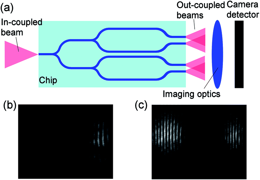 | ||
| Fig. 2 (a) Schematic illustration of the experimental arrangement. Captured interferogram of (b) MIP functionalized, and (c) antibody functionalized sensor chip. | ||
Sensing method is based on the analysis of the sample induced changes in the interferogram fringe positions.22,23 When RI on top of the waveguide is changed by the sample, the effective RI of the waveguide is changed due to the interaction of the sample with the evanescent wave field of the light propagating in the waveguide. The binding of the molecules changes the RI of the layer on top of the waveguides since water is replaced by a material having typically a higher RI. In the designed sensor layouts, sample induced effective RI change differs between the measurement and reference waveguides. This changes their mutual optical path length difference that again shifts the interferogram fringes. The sample induced phase change of the fringes, Δϕ, is23
 | (1) |
![[small script l]](https://www.rsc.org/images/entities/i_char_e146.gif) is the sensing length of the sensor, Δneff,m and Δneff,r are the sample induced effective refractive index changes of the measurement and reference waveguides, respectively, and λ the wavelength of the light. As shown by eqn (1), the induced phase change is inversely proportional to the wavelength that also affects to the probing depth of the evanescent wave field and to the effective refractive index changes of the waveguides. Interferograms captured during the experiments were analyzed by using two dimensional fast Fourier transform (FFT) yielding the phases of the fringes and enabling the calculation of the sensor responses as phase changes.
is the sensing length of the sensor, Δneff,m and Δneff,r are the sample induced effective refractive index changes of the measurement and reference waveguides, respectively, and λ the wavelength of the light. As shown by eqn (1), the induced phase change is inversely proportional to the wavelength that also affects to the probing depth of the evanescent wave field and to the effective refractive index changes of the waveguides. Interferograms captured during the experiments were analyzed by using two dimensional fast Fourier transform (FFT) yielding the phases of the fringes and enabling the calculation of the sensor responses as phase changes.
Materials and methods
Fabrication of sensor chips
Illustration of the cross-section of the inverted ridge waveguide structure used in the sensor chips is shown in Fig. 3(a). The waveguide fabrication is shortly outlined in this paper, and detailed description is given in the earlier paper by the authors.14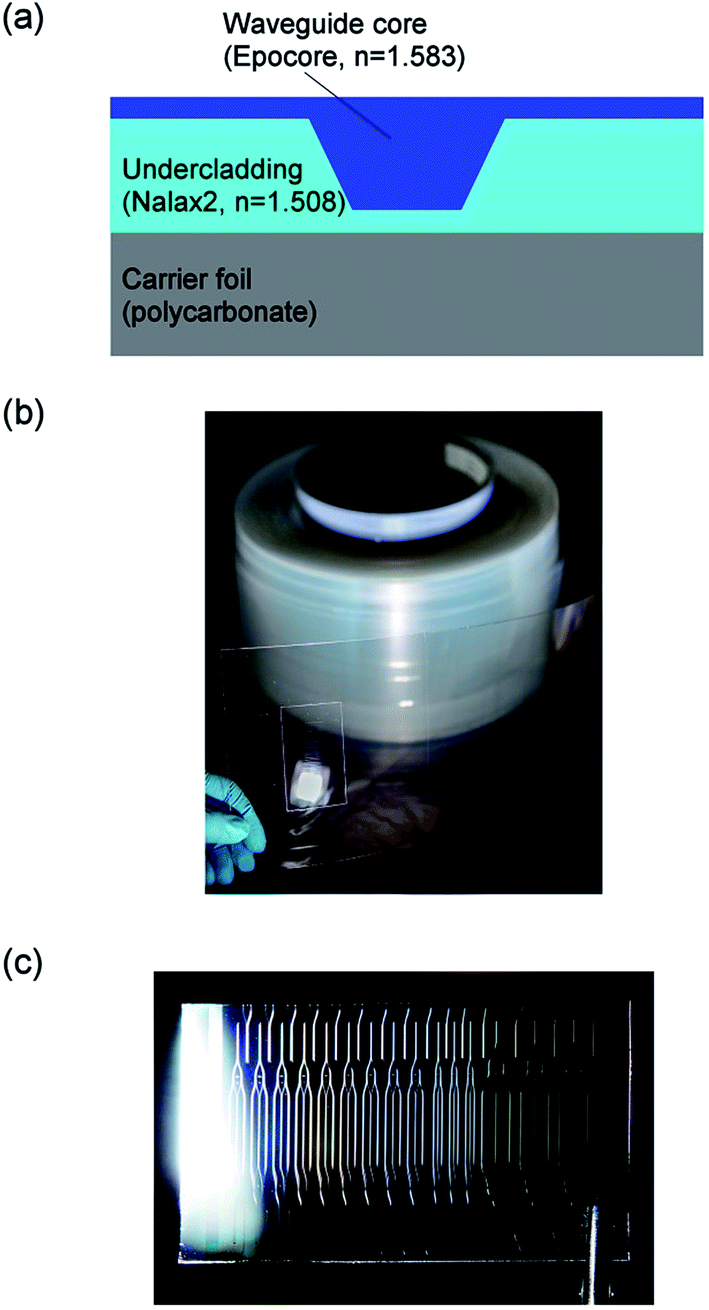 | ||
| Fig. 3 (a) Schematic of the cross-section of the inverted ridge waveguide structure showing the materials and the refractive indices,14n, of the core and undercladding layers at the wavelength of 975 nm, i.e. at the wavelength used in the sensing experiments. (b) Roll of sensor waveguides. (c) Sensor platform cut from the roll. | ||
The fabrication of the waveguides was done in two phases using two R2R units. In the first phase, the waveguide grooves were patterned into the UV-curable acrylate based undercladding material (Nalax2, Nanocomp) using UV-imprinting method, and in the second phase the grooves were filled with the epoxy-based waveguide core material (Epocore, Micro resist technology). In the first phase, the undercladding material was gravure coated onto polycarbonate foil. The waveguide grooves were patterned by pressing a nickel stamp, having a ridge structure, into the uncured undercladding material and curing the material by applying UV-light through the transparent foil. In the second phase, gravure printing method was used to fill the waveguide grooves with the UV-curable waveguide core material followed by curing with UV-light. A roll of R2R produced sensor platforms is shown in Fig. 3(b).
The sensor platforms were cut from the roll for post-processing to sensor chips as shown in Fig. 3(c). The in- and outcoupling facets of the waveguides were formed by cleaving. The overcladding layer (OP-4-20632, Dymax) was patterned onto the chips as required by the different sensor embodiments.
Functionalisation with MIP layer
The MIP- and NIP-layers were applied into the measurement window of YI1 and YI2, respectively, by spin-coating the respective oligomer solutions at 3000 rpm using custom-built spin coater. Oligomers leading to MIP were prepared by dissolving 17 mg dihydroxyethene bisacrylamide (DHEBA; cross-linker), 8 mg methacrylic acid (MAA; functional monomer) and 1.5 mg melamine (template) in 1 ml de-ionized water. Synthesis of NIP followed the same experimental protocol but for adding melamine. This solution was then heated to 55 °C followed by adding 5 mg sodium peroxodisulfate (PODS; radical initiator). Then, polymerization took place until the solution turned slightly turbid. The coated length of the waveguides was 10 mm defined by an opening in the overcladding layer. Prior to interferometric experiments, the melamine template molecules were removed from the MIP layer by immersing the sensor chip into water and shaking it overnight.Functionalisation with antibodies
For multi-analyte biosensing, antibodies for hCG and human-CRP were inkjet patterned onto the measurement waveguides of YI1 and YI2, respectively, and mouse IgG, onto the reference waveguides. Bio-inks containing anti-human CRP antibodies (monoclonal antibody (Mab) 6404, Medix Biochemica), anti-hCG antibodies (Mab 5006, Medix Biochemica) or mouse IgG (ChromPure, Jackson ImmunoResearch Laboratories) were prepared. Each bio-ink contained 1.0 mg ml−1 of the respective antibody prepared in Na2CO3 buffer solution (50 mM, pH 9.6) containing 3% of isopropanol and 0.1% of Tween-20. Inks were filtered through a nylon membrane filter with 0.2 μm pore size to avoid clogging of the inkjet printhead nozzles. Before inkjet printing, the chips were oxygen plasma treated 1 min at 300 W to make surfaces more hydrophilic to improve the printing quality. The printing was done using a piezoelectric inkjet printer (Dimatix DMP-2800, Fujifilm Dimatix). Size of the printed rectangular patterns, shown in Fig. 8(b), was 0.6 × 10 mm2.After inkjet printing, the sensor surface was blocked to reduce unspecific binding during the experiments by applying 500 μl of 3% bovine serum albumin (BSA) (Sigma-Aldrich) in phosphate buffered saline (PBS) buffer (12 mM, pH 7.4) on top of the sensor chips. Chips were shaken for 10 min, after which they were aspirated. The unbound BSA was washed with 500 μl PBS with Tween-20 (PBST) applied on the sensor chips. Chips were shaken for 5 min, after which they were aspirated. During these steps the salts in the bio-inks that dry onto the chip surface during the inkjet printing were washed away.
Sample solutions and their actuation
For chemical sensor experiments, aqueous melamine solutions were prepared by dissolving melamine (Alfa Aesar) in ultrapure water at the following concentrations: 0.1, 0.25, 0.5 and 1.0 g l−1. Melamine concentrations of the sample solutions were chosen to reflect the levels found in contaminated milk powders reported to contain melamine up to 2563 mg kg−1.24For biosensor experiments, sample solutions containing either 2.0 μg ml−1 of human-CRP antigen (BBI Solutions) or 0.9 μg ml−1 (corresponding 100 mIU ml−1) of hCG antigen (Scripps Laboratories) were prepared in 1% bovine serum albumin (BSA) (Sigma-Aldrich) in phosphate buffered saline (PBS) buffer (12 mM, pH 7.4) as a sample matrix. To study the sensing of ambient RI changes, a sample solution was prepared containing 0.5 weight% (wt%) of D-glucose (Sigma-Aldrich) in 1% BSA in PBS buffer. The BSA content of the sample matrix increases its complexity compared to mere buffered saline solution. The concentrations of hCG and CRP in sample solutions were chosen to be physiologically relevant. For hCG, pregnancy tests typically have sensitivities ∼25 IU l−1.25 However, during pregnancy the concentration of hCG in serum can be >300![[thin space (1/6-em)]](https://www.rsc.org/images/entities/char_2009.gif) 000 IU l−1 and in urine >2500 IU l−1 although the levels vary greatly.25 For CRP, the normal concentration in human serum is <8 μg ml−1 but the levels can even 1000 fold in inflammation.26 CRP concentration can also be used to estimate the risk of cardiovascular disease where levels <1 μg ml−1 indicate low, 1–3 μg ml−1 moderate, and >3 μg ml−1 high risk.27
000 IU l−1 and in urine >2500 IU l−1 although the levels vary greatly.25 For CRP, the normal concentration in human serum is <8 μg ml−1 but the levels can even 1000 fold in inflammation.26 CRP concentration can also be used to estimate the risk of cardiovascular disease where levels <1 μg ml−1 indicate low, 1–3 μg ml−1 moderate, and >3 μg ml−1 high risk.27
Flow cell was assembled on top of the interferometer chips at least a day before the measurements, and it was filled with the sample matrix solution. The inlet and the outlet of the flow cell were connected to a sample vial and to a syringe pump (Nexus 3000, Chemyx), respectively, by a tube. Sample and flushing solutions were pipetted into the sample vial sequentially. The syringe pump was driven in withdraw mode at a flow rate of 100 μl min−1 during the chemical sensing experiments and at a flow rate of 20 μl min−1 during biosensing experiments. In the chemical- and biosensing experiments, the sensor response time was limited by the time it took for the sample to replace the preceding fluid within the flow cell, and by the mass transportation of the analyte molecules from the sample volume to the sensor surface. The response time was about 2 min in chemical sensing experiments, and about 5 min in biosensing experiments. The fluid replacement times were different for the chemical- and biosensing experiments due to different flow rates and different flow cell volumes.
Fluorescent staining
For the fluorescent staining of CRP analytes, 13.2 μg ml−1 of anti-CRP antibody (Mab 6405, Medix Biochemica) labelled with Alexa Fluor 546 (Thermo Fisher Scientific) fluorescent label was prepared in 1% BSA in 12 mM PBS buffer (pH 7.4). For the staining of hCG analytes, 6.6 μg ml−1 of anti-hCG antibody (Mab 5014, Medix Biochemica) labelled with Alexa Fluor 546 fluorescent label was prepared in 1% BSA in 12 mM PBS buffer (pH 7.4). For IgG staining, 4.0 μg ml−1 of goat anti-mouse IgG antibodies (Thermo Fisher Scientific) labelled with Alexa Fluor 647 (Thermo Fisher Scientific) fluorescent label was prepared in 1% BSA in 12 mM PBS buffer (pH 7.4).Fluorescent staining was done by using the following procedure: 500 μl of staining solution was pipetted onto the sensor surface, and the chip was placed onto a shaker for 10 minutes. The staining solution was aspirated and 400 μl of PBST solution was pipetted onto the chip to wash the unbound labelled antibodies. The chip was placed onto a shaker for 10 minutes, and PBST solution was aspirated.
Optical setup and stability
Light from a laser source (QFBGLD-980-5, QPhotonics) emitting at the wavelength of 975 nm was end-fire coupled into the input waveguide of a sensor chip by using a tapered polarization maintaining fibre (spot size of ∼2.8 μm). The chosen wavelength enabled the single-mode operation of the waveguides14 as well as the use of a silicon-based camera. An optical isolator was used to prevent the disturbing reflections back to the laser. The sensor experiments were conducted using TM polarized light reported to have a higher sensitivity than TE polarization.6Interferograms were imaged onto a camera detector (UI-3240CP-NIR-GL, IDS Imaging Development Systems) using a 40× microscope objective. The imaging was done at the distance of ∼200 μm from the out-coupling end of the chip. The camera was located ∼17 cm from the chip. The interval between the captured interferograms was 2 s during the chemical sensing experiments and 10 s during biosensing experiments.
Stability of the sensing system was studied by measuring phase changes while the sample matrix was flowing through the flow cell. Measured phase change curves for MIP and antibody functionalized chips are shown in Fig. 4 as well as lines fitted to the data points showing the trend of the system drift. In the curves, the noise of the system is seen as the small scale variation of the phase changes in the range of milliradians. The larger fluctuations and the overall drift of the phase change curves were attributed to the mechanical and thermal instabilities of the sensor chip and the experimental setup. The phase change fluctuations were less than 0.1 radians being thus much smaller than the analyte induced phase changes that were in the range of radians. It can be also seen that in all of the cases the trend of the drift was below 0.01 rad min−1 that is less than responses induced by the analytes in the sensing experiments.
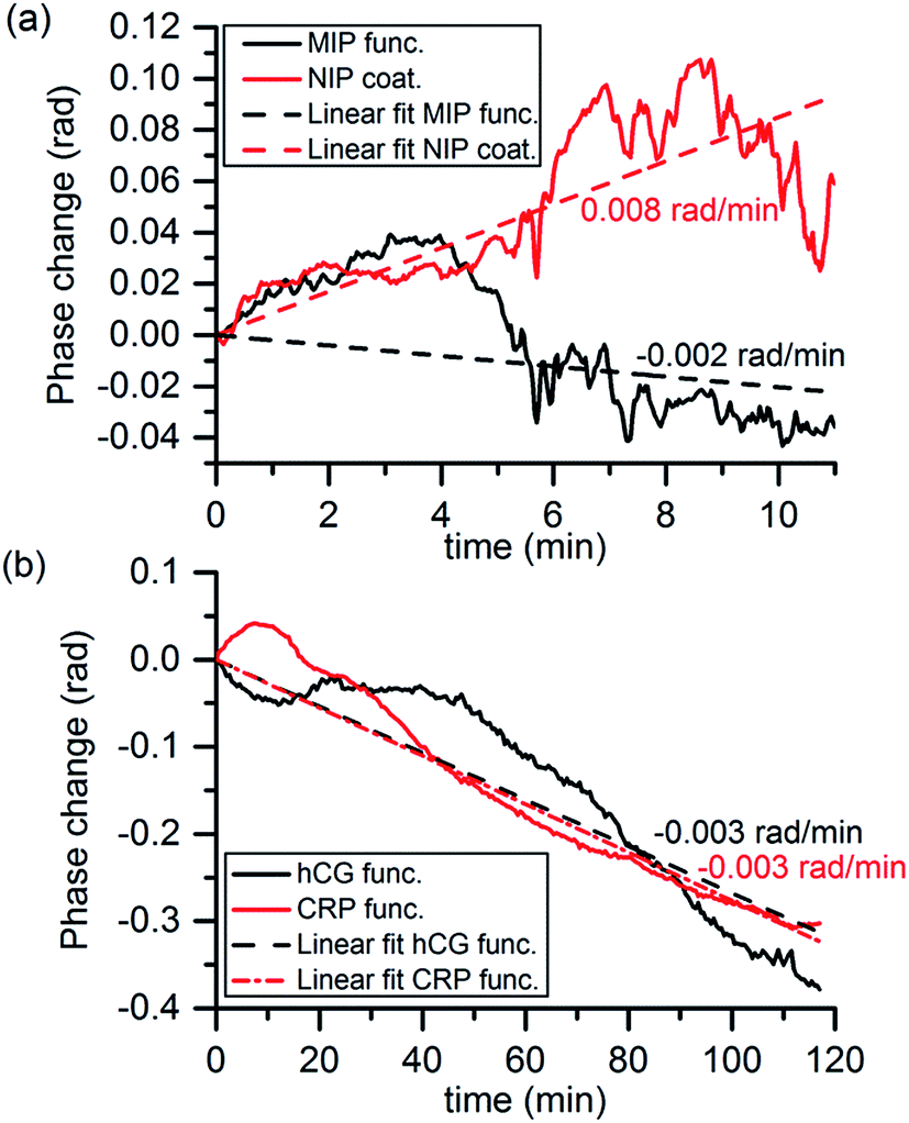 | ||
| Fig. 4 Phase change curves measured while the sample matrix flowed in the flow cell, and lines fitted to the data points for (a) MIP functionalized chip (image interval 2 s), and (b) for antibody functionalized chip (image interval 30 s). The slope of the fitted lines is also shown indicating the trend of the system drift. | ||
Results
Chemical sensor
To demonstrate the chemical sensing, a MIP-functionalized sensor chip was exposed to aqueous melamine solutions. Each concentration was measured three times by flowing 500 μl of the melamine solution through the flow cell followed by flushing with water until the end of the measurement leading to 5 min analyte exposure. Timing pattern of the solutions in the flow cell is indicated in Fig. 5.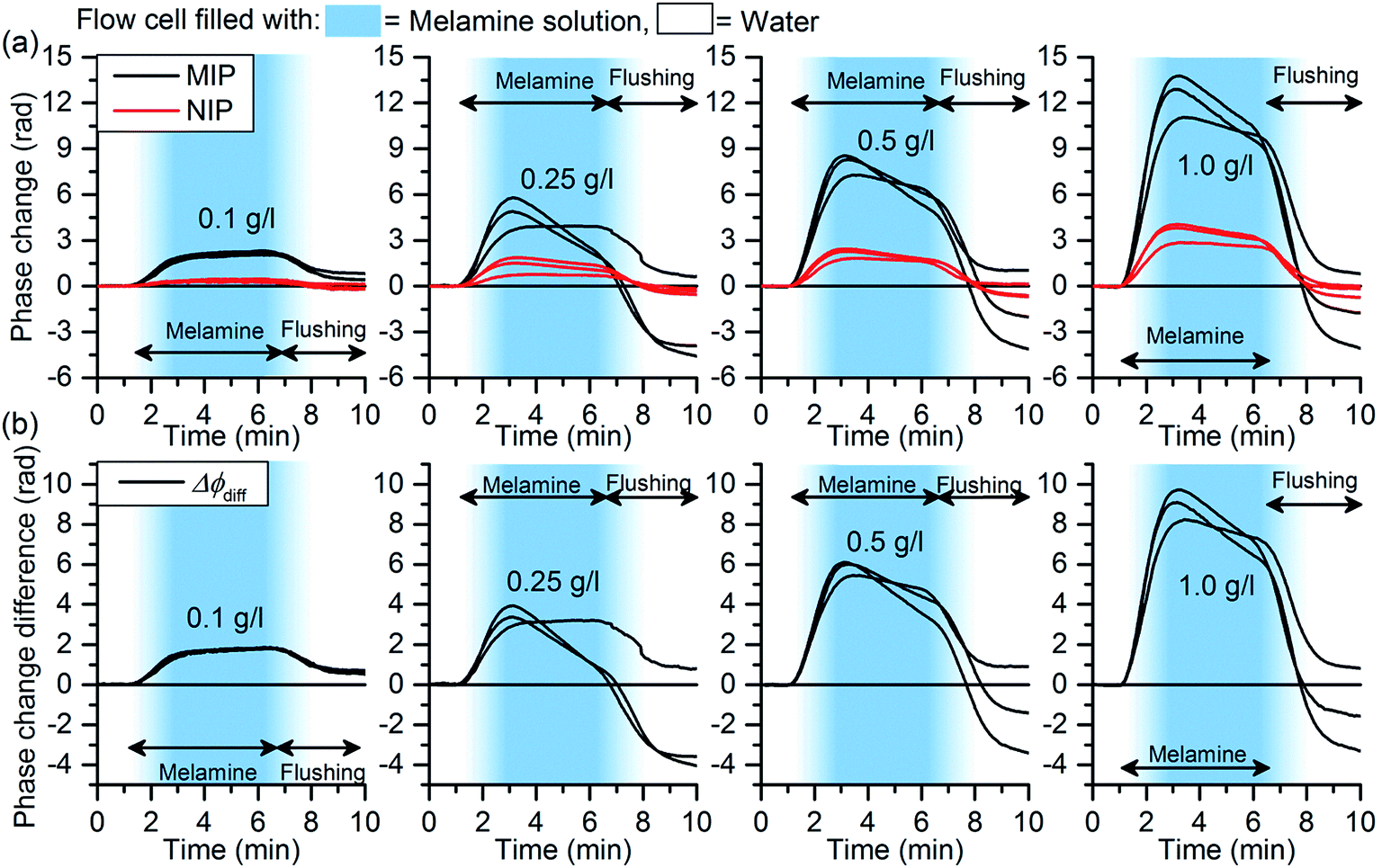 | ||
| Fig. 5 (a) Phase change curves of MIP functionalized YI1 and NIP coated YI2 measured at various melamine concentrations. Each concentration (value shown next to the curves) was measured three times. (b) Δϕdiff curves showing the net difference of the phase change values between the MIP functionalized YI1 and NIP functionalized YI2 at different melamine concentrations. Timing of the solutions in the flow cell is indicated by the arrows and the background colour. | ||
Due to the patterned functionalization of the chip, the MIP functionalized interferometer was measuring the specific binding and the NIP coated interferometer the non-specific binding of melamine to the polymer layers. Both interferometers were also measuring the bulk effects of the sample solutions. The shift of the interference fringes during an experiment is shown in Fig. 6. The phase change curves of the MIP and NIP coated interferometers, i.e. ΔϕMIP and ΔϕNIP, respectively, are shown in Fig. 5(a). The phase change curves were first analysed from the interferograms and were subsequently baseline corrected based on the values between 0 and 1.1 min. The curves clearly show that the MIP coated interferometer undergoes significantly higher phase changes on exposure to melamine: they are exceeding those of the corresponding NIP by roughly a factor of four. This gives clear evidence that incorporation of the melamine into the cavities of the MIP leads to substantial measurable phase change.
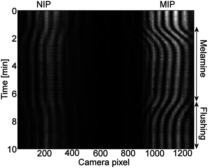 | ||
| Fig. 6 Shift of the interferogram fringes during a chemical sensing experiment conducted with the melamine concentration of 1.0 g l−1. Figure is constructed by first selecting the same narrow section (height 5 pixels) across each of the time laps images captured during the experiment, and then combining these sections. | ||
The measured phase changes also clearly exceed the values that would be produced by the mere bulk refractive index differences of the melamine solutions to pure water. The phase change Δϕbulk induced by the bulk RI difference of the sample solutions to pure water, Δn, was evaluated by using formula
 | (2) |
The actual imprinting effect can be assessed by calculating the net difference of the phase change values, Δϕdiff, between the MIP and NIP coated interferometers, i.e. Δϕdiff = ΔϕMIP − ΔϕNIP, shown in Fig. 5(b). It is worth noticing that the calculation of the difference signal eliminates the phase changes related to internal changes at the chip that both YIs see similarly. These kinds of changes may be induced, for example, by temperature variations. However, the capability of the method to eliminate the chip internal changes was not separately assessed by experiments.
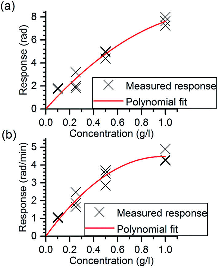
Responses were determined from Δϕdiff, curves by (1) calculating the height of the phase change step by taking the average of the values within 5.0–5.3 min, and (2) by determining the slope of the phase change curves within 2.0–2.8 min. The responses and the second order polynomials fitted to the data points are shown in Fig. 7(a) and (b). In the fitting, the limit of detection was not taken into account since it was not assessed by the experiments. As can be seen, the sensor responses in overall increase with increasing melamine concentration demonstrating the capability of MIP functionalized chip to chemical sensing. The slope-based method was capable to differentiate between the two lowest concentrations whereas the step height-based method could not differentiate between these two. The results show beginning saturation for melamine concentrations above 0.5 g l−1, which is in line with previous MIP studies aiming at detecting small molecules.30 The reason for such saturation behavior can be found in the recognition mechanisms of MIP: analyte incorporation is the result of thermodynamic equilibrium between analyte molecules bound in recognition sites of the MIP and those in solution. Both the amount of binding sites within a MIP layer and accessibility of diffusion pathways within the matrix are limited hence limiting the dynamic range of the sensors. The slope-based method enables faster signal quantification than the method based on the step height that is an advantage for rapid diagnostics. The slight decrease in the sensor responses seen in the ΔϕMIP and ΔϕNIP curves of Fig. 5(a) with time can most probably be appointed loss of a few percent of the film as well as to minimal irreversible binding of melamine by the films. However, this does not affect the difference signal and hence can be neglected.
 | ||
| Fig. 7 Calculated responses and lines fitted to the data points based on (a) the phase change step height, and (b) the slope of the rising edge of Δϕdiff curves. | ||
Multi-analyte biosensor
To demonstrate the multi-analyte biosensing, three antibody-functionalized chips were sequentially exposed to 400 μl of hCG and CRP sample solutions separated by a flushing step with 300 μl of the sample matrix leading to 20 min analyte exposure followed by 15 min sample matrix exposure. The timing of the solutions in the flow cell is indicated in Fig. 8(a).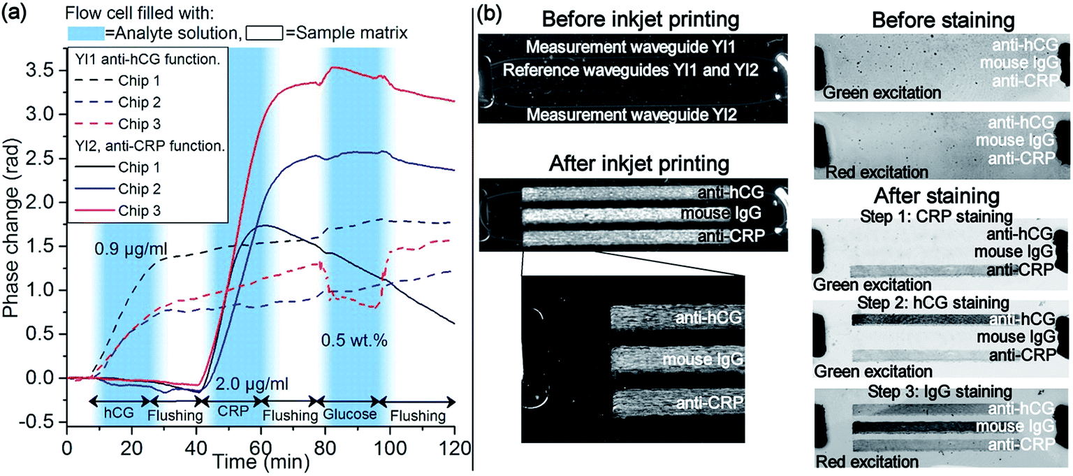 | ||
| Fig. 8 (a) Phase change curves showing the specific responses of YI1 (dashed lines) and YI2 (solid lines) to hCG and human CRP samples, respectively. Responses to glucose solution demonstrate the sensor sensitivity to ambient RI changes. (b) Left: Microscope images of the YI chip before and after the antibody functionalization by inkjet printing showing the printed areas on top of the waveguides. Printed areas are visible due to the salts in the bio-inks that dry onto the chip surface. Right: Verification of specific binding of analytes onto the inkjet printed areas by fluorescent staining and imaging. The fluorescence images (the darker the colour the higher the fluorescence intensity) taken before staining show no fluorescence from the printed areas. After each staining step, the corresponding inkjet printed area became fluorescent verifying the localized presence of the analytes and the reference IgG coating. | ||
With the chosen antibody functionalization schema, the antibody coating on the measurement waveguide makes it specifically bind its target analyte onto the sensor surface whereas the IgG-coated reference waveguide takes into account unspecific binding. Since all the sensor waveguides are exposed similarly to the solutions in the measurement window, in theory, the ambient RI change should not induce any phase difference between the measurement and the reference waveguides, and thus also not lead to measurable signal. Therefore, the measured phase change signal can be assumed to directly show the difference between the binding of the analytes on the measurement and the reference waveguides in real-time. In addition, the similarity of the measurement and reference waveguide structures makes them react similarly to temperature changes reducing the temperature sensitivity of the sensor.
The phase change graphs, shown in Fig. 8(a), were analysed from the captured interferograms and were subsequently baseline corrected based on the values between 0 and 5.7 min following the same procedure with melamine measurements. In each of the three experiments, YI1 shows a clear phase change signal when the sensor was exposed to hCG sample, whereas the curve of YI2 remains nearly unchanged. Similarly, when the sensor was exposed to CRP sample, the phase change curve of YI2 shows a clear phase change signal whereas the curve of YI1 remains unchanged. This indicates that analytes were selectively binding to the receptor layers on the measurement waveguides. During the following flushing steps, the phase change curves level off, indicating that no more analyte molecules were binding onto the surface.
Sensor responses to the hCG and CRP samples were determined from the phase change curves by calculating the average value within 35–38 min for YI1, and within 68–71 min for YI2, i.e. during the flushing step following the analyte exposure. The average response of the three measurements of YI1 to hCG samples was 1.0 rad and the range of the response values was 0.6 rad. Similarly the average response of YI2 to CRP samples was 2.5 rad and the range 1.7 rad. The responses to both analytes varied substantially from chip to chip. This was attributed to variations in the inkjet printed functionalization layers on the waveguides, such as the layer thickness and the amount of capture antibodies, causing also variation in intensity of the fluorescence signal in Fig. 8(b).
As discussed above, the chosen antibody functionalization schema should desensitize the sensor to ambient RI changes. To study sensitivity to ambient RI changes, chips were exposed to 400 μl of 0.5 wt% glucose solution followed by flushing with the sample matrix. Timing of the solutions is shown in Fig. 8(a). It can be seen that in all but one of the phase change curves, the response to the ambient RI change is significantly smaller than the value of ∼1 rad reported earlier by the authors for polymeric R2R fabricated non-functionalized YI sensor chips for aqueous glucose solution having the same concentration. The larger phase change signal of one of the curves, ∼0.5 rad, is most likely caused by the different thicknesses of the inkjet-printed antibody layers on the measurement and reference waveguides causing a different penetration of the evanescent wave fields into the sample volume and thus different change of the effective RIs. Although the chosen functionalization schema could not render the sensors completely insensitive to the ambient RI changes, the effect was nonetheless suppressed.
After the interferometric measurements, fluorescent staining and imaging was used to verify the specific binding of the analytes to the correspondingly functionalized areas, as well as the presence of IgG on the reference waveguides. Fluorescently labelled antibodies were used to stain CRP and hCG analytes (green fluorescence excitation) and IgG (red fluorescence excitation) in three sequential steps. The fluorescence images of Fig. 8(b) show no fluorescence signal from the printed areas before staining. During each staining step, the corresponding inkjet functionalized area became fluorescent, as shown in Fig. 8(b), proving the presence of CRP, hCG and IgG at these areas, and confirming the results of interferometric measurements. However, when investigating the fluorescent areas in detail, it can be observed that fluorescent intensity is not uniform. This indicates that the variations in the inkjet printed functionalization layers lead to fluctuating amounts of bound analyte molecules resulting in variation of the response values of biosensor experiments.
Discussion
In this paper we reported for the first time analyte specific sensing using integrated YI sensor chips having R2R mass-fabricated polymeric single-mode waveguides. We demonstrated proof-of-concept for chemical sensing of small molecules using MIP receptor layer, and for multi-analyte detection of biomolecules using inkjet printed antibody-based receptor layers. The model analytes chosen for the demonstrations have substantial interest: melamine has become an important analyte in food adulteration, whereas both hCG and CRP are important clinical parameters: the former is an early stage pregnancy marker, the latter an unspecific inflammation marker and an indicator for the assessment of the risk of cardiovascular disease.The MIP functionalized chip was shown to be capable to measure melamine concentrations quantitatively having linear responses below the concentration of 0.5 g l−1 and beginning saturation at the higher concentrations. In the case of the antibody functionalized chip, the responses to both analytes varied substantially from chip to chip. Thus the sensor responses at the moment only qualitatively indicate the presence or absence of the analytes and no quantitative responses were obtained. Deviating responses with the antibody-functionalized chips were attributed to variations in the inkjet printed functionalization layers on the waveguides. These are related to reproducibility of layer thickness and the amount of active capture antibodies. The repeatability of the sensor responses is most likely improved if the capture antibodies are bound to waveguide surface oriented and are forming mono layers.
To further characterize the sensor chip properties, the limit of detection, limit of quantification and repeatability of the sensor responses need to be studied by conducting experiments with large number of sensor chips. In addition, to assess the applicability of the sensors for real-life applications, experiments need to be conducted with real samples in realistic experimental conditions.
Conclusions
In conclusion, we demonstrated that disposable polymeric YI sensor chips are applicable for analyte specific chemical sensing of small molecules, and for multi-analyte detection of biomolecules. The MIP functionalized sensor chip indeed revealed responses depending on melamine concentration, which is the first demonstration of MIP on a low-cost, polymer-based sensor device for direct RI sensing. The antibody-functionalized YI sensor chips demonstrated the applicability of patterned, inkjet printed receptor layers for specific multi-analyte detection showing qualitative indication of the presence or absence of the analytes.Proving the concept of disposable, low-cost sensor systems thus inherently opens up scientifically and economically interesting strategies for portable sensing and analysis. This ranges from determining the quality of food at home or providing low-cost diagnostic tests for rapid evaluation of important clinical parameters directly at the point-of-care.
Development of low-cost sensor solutions is one of the main challenges in the sensor field. Demonstration of the analyte specific chemical- and biosensing with disposable polymeric YI sensor chips using artificial and biological receptor layers opens new avenues for sensor implementation.
Acknowledgements
Authors acknowledge financial support by the European Commission via the Seventh Framework Programme under the grant agreement No. 263382 “PHOTOSENS”, and by Academy of Finland grant No. 284907. Authors also acknowledge the assistance of J. Ollila, VTT, in preparing the sensor chips.Notes and references
- D. E. W. Patabadige, S. Jia, J. Sibbitts, J. Sadeghi, K. Sellens and C. T. Culbertson, Anal. Chem., 2016, 88, 320 CrossRef CAS PubMed.
- Y. Chen, L. Jiang, M. Mancuso, A. Jain, V. Oncescu and D. Erickson, Nanoscale, 2012, 4, 4839 RSC.
- P. Kozma, F. Kehl, E. Ehrentreich-Förster, C. Stamm and F. F. Bier, Biosens. Bioelectron., 2014, 58, 287 CrossRef CAS PubMed.
- A. Ymeti, J. S. Kanger, R. Wijn, P. V. Lambeck and J. Greve, Sens. Actuators, B, 2002, 83, 1 CrossRef CAS.
- K. Schmitt, B. Schirmer, C. Hoffmann, A. Brandenburg and P. Meyrueis, Biosens. Bioelectron., 2007, 22, 2591 CrossRef CAS PubMed.
- M. Wang, J. Hiltunen, C. Liedert, L. Hakalahti and R. Myllylä, J. Eur. Opt. Soc., Rapid Publ., 2012, 7, 12019 CrossRef.
- A. Brandenburg and R. Henninger, Appl. Opt., 1994, 33, 5941 CrossRef CAS PubMed.
- G. H. Cross, A. A. Reeves, S. Brand, J. F. Popplewell, L. L. Peel, M. J. Swann and N. J. Freeman, Biosens. Bioelectron., 2003, 19, 383 CrossRef CAS PubMed.
- J. Xu, D. Suarez and D. S. Gottfried, Anal. Bioanal. Chem., 2007, 389, 1193 CrossRef CAS PubMed.
- A. Schimpf, D. Bucci, M. Nannini, A. Magnaldo, L. Couston and J.-E. Broquin, Sens. Actuators, B, 2012, 163, 29 CrossRef CAS.
- G. H. Cross and Y. Ren, J. Appl. Phys., 1999, 86, 6483 CrossRef CAS.
- M. Wang, S. Uusitalo, C. Liedert, J. Hiltunen, L. Hakalahti and R. Myllylä, Appl. Opt., 2012, 51, 1886 CrossRef CAS PubMed.
- M. Hiltunen, J. Hiltunen, P. Stenberg, S. Aikio, L. Kurki, P. Vahimaa and P. Karioja, Opt. Express, 2014, 22, 7229 CrossRef PubMed.
- S. Aikio, J. Hiltunen, J. Hiitola-Keinänen, M. Hiltunen, V. Kontturi, S. Siitonen, J. Puustinen and P. Karioja, Opt. Express, 2016, 24, 2527 CrossRef PubMed.
- A. Ymeti, J. S. Kanger, J. Greve, G. A. J. Besselink, P. V. Lambeck, R. Wijn and R. G. Heideman, Biosens. Bioelectron., 2005, 20, 1417 CrossRef CAS PubMed.
- A. Ymeti, J. Greve, P. V. Lambeck, T. Wink, S. W. F. M. van Hövell, T. A. M. Beumer, R. R. Wijn, R. G. Heideman, V. Subramaniam and J. S. Kanger, Nano Lett., 2007, 7, 394 CrossRef CAS PubMed.
- L. Uzun and A. P. F. Turner, Biosens. Bioelectron., 2016, 76, 131 CrossRef CAS PubMed.
- P. L. Edmiston, D. P. Campbell, D. S. Gottfried, J. Baughman and M. M. Timmers, Sens. Actuators, B, 2010, 143, 574 CrossRef CAS.
- S. M. Reddy, D. M. Hawkins, Q. T. Phan, D. Stevenson and K. Warriner, Sens. Actuators, B, 2013, 176, 190 CrossRef CAS.
- J. T. Kirk, G. E. Fridley, J. W. Chamberlain, E. D. Christensen, M. Hochberg and D. M. Ratner, Lab Chip, 2011, 11, 1372 RSC.
- N. Komuro, S. Takaki, K. Suzuki and D. Citterio, Anal. Bioanal. Chem., 2013, 405, 5785 CrossRef CAS PubMed.
- A. Ymeti, J. S. Kanger, J. Greve, P. V. Lambeck, R. Wijn and R. G. Heideman, Appl. Opt., 2003, 42, 5649 CrossRef CAS PubMed.
- J. S. Kanger, V. Subramaniam, P. H. J. Nederkoorn and A. Ymeti, in Advanced Photonic Structures for Biological and Chemical Detection, ed. X. Fan, Springer, Dordrecht, Heidelberg, London, New York, 2009, ch. 10, pp. 265–295 Search PubMed.
- J. Liu, A. Ren, L. Yang, J. Gao, L. Pei, R. Ye, Q. Qu and X. Zheng, Can. Med. Assoc. J., 2010, 182, 439 CrossRef PubMed.
- M. Montagnana, T. Trenti, R. Aloe, G. Cervellin and G. Lippi, Clin. Chim. Acta, 2011, 412, 1515 CrossRef CAS PubMed.
- K. D. McClatchey, S. Alkan and E. Hackel, Clinical Laboratory Medicine, LWW, Philadelphia, PA, 2nd edn, 2001 Search PubMed.
- P. M. Ridker, Texas Heart Institute Journal, 2005, 32, 384 Search PubMed.
- W. Heller, J. Phys. Chem., 1965, 69, 1123–1129 CrossRef CAS.
- D. R. Lide, CRC Handbook of Chemistry and Physics, CRC, Boca Raton, FL, 83rd edn, 2002 Search PubMed.
- R. Suedee, W. Intakong, P. A. Lieberzeit, P. Wanichapichart, P. Chooto and F. L. Dickert, J. Appl. Polym. Sci., 2007, 106, 3861 CrossRef CAS.
| This journal is © The Royal Society of Chemistry 2016 |