
High efficiency CdTe solar cells with a through-thickness polycrystalline CdTe thin film
Kai Shenab,
Zhizhong Baia,
Yi Denge,
Ruilong Yanga,
Dezhao Wanga,
Qiang Lia and
Deliang Wang*acd
aHefei National Laboratory for Physical Sciences at the Microscale, University of Science and Technology of China, Hefei, Anhui 230026, People's Republic of China. E-mail: eedewang@ustc.edu.cn
bDepartment of Electronic Engineering, College of Information Science and Technology, Jinan University, Guangzhou 510632, People's Republic of China
cCAS Key Laboratory of Energy Conversion Materials, University of Science and Technology of China, Hefei, Anhui 230026, People's Republic of China
dNational Synchrotron Radiation Laboratory, University of Science and Technology of China, Hefei, Anhui 230029, People's Republic of China
eSchool of Electronic and Information Engineering, Hankou University, Wuhan 430212, People's Republic of China
First published on 20th May 2016
Abstract
The absorber layer in a CdTe solar cell is made of a polycrystalline CdTe thin film with a thickness of several μm. It is highly desirable that the CdTe film could be made of through-thickness CdTe grains. In such a case, the photon-generated carriers could be transported to the positive and negative contacts without encountering any grain boundaries in CdTe, thus significantly reducing the carrier scattering/recombination occurring at the grain boundary. We propose and demonstrate that one of the most important roles for the presence of oxygen during the CdTe film growth is to in situ form a low-melting liquid mixture of oxides (CdTeOx, TeOx and CdOx), Te, and CdTe on the growth front of the CdTe grain surface. This liquid mixture, having a thickness of ∼50 nm, assists material transport from the vapor through the liquid to the liquid–solid interface, where Cd, Te, and Cd–Te molecules reacted to epitaxially deposit on the CdTe growth front. Assisted by a highly crystalline mono-grained CdS window layer template, CdTe preferential growth with through-thickness grains along the normal direction of the film has been achieved. CdTe solar cells fabricated with such CdTe absorbers demonstrate much enhanced external quantum efficiency, and cells with efficiencies as high as 14–15.2% have been fabricated.
1. Introduction
The thin film CdTe solar cell is a competitive photon-to-electric energy conversion device. In the past two decades, in addition to the market-dominating Si-based photovoltaic products, CdTe solar cell has been the most successful thin-film photovoltaic product in the photovoltaic market with regards to both its large-scale commercialization and module price. Remarkable progress has been made in the last several years, and the highest small-area cell efficiency has been increased from 16.7 to 22.1%.1,2 The absorber layer in a CdTe solar cell is a polycrystalline CdTe thin film with grain size in the micrometer scale.3,4 High crystalline quality CdTe films can be fabricated by using physical deposition techniques, such as close-spaced sublimation, radio frequency magnetron sputtering, vapor transport deposition, and thermal evaporation; or by using chemical deposition, such as electro-chemical deposition.5 Usually a CdTe thin film fabricated by a physical deposition technique at high substrate temperature has large CdTe grain size in micro-meter scale, and that fabricated by a chemical deposition technique has smaller CdTe grains. CdTe thin films prepared by both the physical and the chemical techniques need to be heat treated in the presence of CdCl2 to activate the electrical property of a CdTe absorber. This activation process is especially necessary for CdTe films prepared by a chemical technique. CdTe thin films prepared by this method usually have CdTe grain size in nanometer or sub-micrometer scale. The main role for the CdCl2 process is the grain growth from nanometer to micro-meter size.6,7During the CdTe deposition and the CdCl2 activation processes, oxygen is usually intentionally introduced into the process atmosphere and regarded as beneficial for high-efficiency CdTe solar cell fabrication. The role of oxygen has been suggested by different researchers to have different effects on both the structural and the electrical properties of a CdTe solar cell employing CdS as the window layer. On the structural effect, it has been reported that the presence of oxygen increased CdTe film nucleation seed density at its initial growth stage, reduced defects and pinhole formation, and suppressed the excessive inter-diffusion at the CdS/CdTe junction. On the electric effect, it has been reported that the presence of oxygen increased charge carrier mobility and carrier lifetime, and passivated the defects at the grain boundary.8–14
Even though it is widely accepted that the presence of oxygen in a CdTe film is important for high efficiency CdTe solar cell fabrication, the role of oxygen in a CdTe solar cell has long been a subject of extensive discussions. In this study we propose and demonstrate that the most important role of oxygen was that it reacted in situ with Te and CdTe to form a low-melting liquid mixture during the growth of a CdTe film. This liquid mixture on the surface of each individual CdTe grain assisted material transport from the vapor to the grain growth front and resulted in preferential growth along the normal direction of the film surface. This important discovery can be employed to clarify several key questions related to the CdTe absorber layer in a CdTe thin film solar cell.
Theoretically, CdTe polycrystalline thin films with through-thickness grains are highly desirable for the fabrication of a high efficiency CdTe solar cell. If the CdTe absorber layer is made of through-thickness grains, photo-generated carriers near the p–n junction would transport in CdTe thin film without encountering any grain boundaries parallel to the film surface. This current transport scenario would significantly reduce the carrier scattering and recombination at grain boundaries.15 In situ introduction of O into a CdTe absorber layer during the CdCl2 treatment, led not only to an order of magnitude increase in the amount of O but also to an enhanced chlorine concentration in CdTe. Part of the O and the Cl were electrically active and formed electrically active complexes, thus significantly enhanced the cell device performance.12 The much increased CdTe grain growth and O/Cl concentration in CdTe during the CdCl2 treatment, which is usually carried out at a temperature of ∼400 °C, indicate that the presence of oxygen during the CdTe growth and CdCl2 treatment played an important role in the atom transportation/reaction.16 So the question is, can we fabricate CdTe thin films with through-thickness grains by employing enhanced material transport with the presence of oxygen? In this study, we propose and demonstrate that one of the most important roles for the presence of oxygen during the CdTe film growth was to in situ form a low-melting liquid mixture of oxides, Te, and CdTe on the growth front of individual CdTe grain surface. This liquid mixture assisted the material transport and liquid-phase assisted CdTe film growth was achieved.
2. Experimental
The polycrystalline CdTe thin films with a thickness of ∼4 μm were prepared by the close-spaced sublimation technique (CSS) in a home-made film-deposition system.3 In order to fabricate CdTe films with through-thickness grains, the oxygen pressure was varied based on our previous study.17 The CdTe films were deposited in an argon–oxygen mixed ambient with different oxygen pressures as given in the following paragraphs. The total mixed pressure was the same, namely, 2 kPa. In this study, in order to provide a well structured template to grow CdTe films with preferential growth along the normal direction of the film, we developed a technology to fabricate CdS films with a mono-grained layer having grain size in submicron, namely, the CdS window layer was composed of only one layer of single CdS grains, which were densely packed along the CdS/FTO interface and had well-defined crystalline facets.4 The microstructure of a mono-grained CdS film on FTO/glass is shown in Fig. 1(a). The CdS precursor films were first dip coated with a saturated CdCl2–methanol solution, and then heat treated in a mixed atmosphere of CdCl2 and air for 10 min at a temperature of 410 °C. The CdTe solar cells fabricated in this study have a cell structure of glass/SnO2:F(FTO)/n-CdS/p-CdTe/backcontact/electrode.3,4 All the CdS/CdTe stacked device film structures were activated at 400 °C for 10 min with the presence of CdCl2 in the air atmosphere. Before the metal electrode film was deposited, the CdTe film surface was first chemically etched in a nitric-phosphoric (NP) solution. Cu/Au bilayer back contacts were prepared by successive thermal evaporation of Cu and Au in a vacuum chamber. The CdTe solar cells size was 4 × 4 mm2.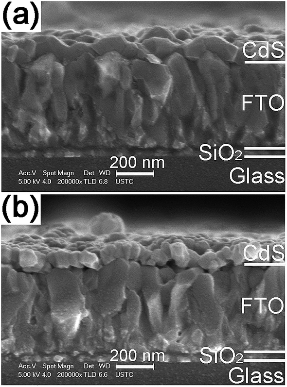 | ||
| Fig. 1 SEM cross-sectional morphologies of (a) the CdS film, which was first coated with a CdCl2 thin layer and then heat treated in a mixed atmosphere of CdCl2 and the air, (b) the CdS film heat treated in a mixed atmosphere of CdCl2 and the air without the coating of a CdCl2 thin layer. | ||
The film morphological microstructures were characterized by using a field emission scanning electron microscope (SEM, Sirion 200). The solar cell current–voltage (J–V) curves were measured under standard AM1.5 illumination (1 kW m−2, 25 °C) using a solar simulator (Oriel Sol 3A, USA). X-ray diffraction (XRD) measurements were carried out by using a TTR-III X-ray diffractometer, with the Cu Kα as the radiation. XPS measurements were performed on a Thermo VG Scientific ESCALAB 250 instrument with Al Kα as the X-ray source. All the XPS spectra were calibrated by using the carbon 1s peak (284.8 eV). The external quantum efficiencies (EQE) of the devices were measured by using a HYPER mono-light System (Bunkoukeiki SM-250).
3. Results and discussions
In general, the micro-structural morphology of a film depends critically on both the substrate structure and the growth condition.18,19 In this study, in order to achieve preferential growth with through-thickness CdTe grains in the normal direction of the film, we prepared CdS films with a mono-grained layer with large-sized and well-crystallized CdS grains, which had an in-plane size of 100–200 nm.4 The as-prepared CBD CdS films were first coated with a thin layer of CdCl2 through dipping in a saturated CdCl2–methanol solution, and then they were heat treated in a mixed atmosphere of CdCl2 and air for 10 min. The SEM cross-sectional structure of a CdS film is shown in Fig. 1(a). It can be seen that the FTO/glass substrate was uniformly and conformally covered with a mono-grained CdS layer with grain size in the sub-micrometer size. This heat treatment had the following beneficial effects on the CdS films and the subsequent CdTe growth. (1) Excessive oxidation on the CdS surface could be avoided, this ensured an appropriate CdTe nucleation and subsequent grain coalescence; (2) very good structure conformity was achieved between the CdS and the FTO electrode, see Fig. 1(a), this would dramatically reduce the pinhole formation in CdTe thin film and this was beneficial for film preferential growth;20 (3) CdS films with the main hexagonal phase, which had a texture structure of H(002), was obtained.4 Such a kind of CdS film with a mono-grained layer provided an ideal template for the subsequent CdTe growth. The initial CdTe crystalline nucleation islands on the CdS H(002) atomic plane could easily coalescence to form large CdTe grains with preferential (111) atomic planes parallel to the film growth surface.21 Another important requirement for achieving through-thickness grain preferential growth is that efficient material supply must be achieved and the atoms reached to the grain growth front must consolidate/react on the right lattice sites without distorting the perfect crystalline growth. In our previous study, we found that at the presence of oxygen, after heat treatment, with or without the presence of CdCl2, at a temperature higher than ∼450 °C, the CdTe film surface was covered by a low-melting eutectic mixture of CdTe, oxides of CdTe and Te.17 So the questions are, is it possible that a liquid mixture can be formed during the CdTe growth with the presence of oxygen? Is it possible to employ this liquid mixture to achieve the vapor–liquid–solid like growth? In this study, we proposed that it is highly possible that a low-melting liquid layer may be formed in situ at the growth front of a CdTe film grown by the close-spaced sublimation technique, where oxygen is present and the growth temperature is relatively high (∼550 °C). The liquid layer can assist the adsorption of the Cd and Te elements from the vapor. The adsorbed Cd and Te atoms are then efficiently transported through the liquid layer to the liquid/solid CdTe interface, whether in the form of elements or chemically bonded molecules, and where they epitaxially deposit on the CdTe lattice. In this study, in order to verify this growth scenario, we increased the oxygen partial pressure PO2 to a value of 0.3 kPa. Another set of CdTe cells was grown with a lower oxygen partial pressure PO2 of 0.1 kPa. The total pressure of argon and oxygen was kept the same, namely, the Ptotal was 2 kPa.3,4,22,23At high film growth temperature around 550 °C, the growing CdTe surface may be instantly oxidized. In order to verify this hypothesis, XPS depth-dependent profile of a CdTe film fabricated under high oxygen atmosphere PO2 of 0.3 kPa was carried out. The XPS spectra for Cd, Te, and oxygen with the etching depth down from the CdTe surface are shown in Fig. 2. The spectra were measured after different Ar+ ion etching time. It can be seen that there was a strong Te–O bonding peak near the CdTe surface region, and its intensity deceased to an almost undetectable value at a depth of ∼60 nm from the surface. The peak of Cd 3d of the Cd–O bonding could not be separately identified due to the similar bonding energy with that of the Cd–Te bonding, whose peak energy was about 0.1–0.8 eV higher.24 But the presence of the Cd–O bonding shifted the Cd 3d peak to lower energy, see Fig. 2(b), inducing asymmetry in the Cd 3d spectrum.25 With increased depth from the surface, the peak asymmetry disappeared, indicating that the peak was mostly contributed by the Cd–Te bonding. The XPS data indicated that the ratio of Cd/Te in the liquid mixture was high at the surface region and low near the liquid/crystalline CdTe interface. This concentration difference was the driving force for the material transport. The intensity of the oxygen O 1s peak, see Fig. 2(c), decreased quickly with the etching depth into the film, and this correlated well with the decreased Te–O peak shown in Fig. 2(a). The variation of the atomic concentration of the Te, which was bonded with oxygen, and the ratio of Cd/Te, with the depth from the CdTe surface are shown in Fig. 2(d). It can be seen that at the surface the ratio of Cd/Te was ∼1.3, much higher than the presumed stoichiometric value of 1. It should be noted that XPS is a semi-quantitative technique to analyze atomic concentration, the uncertainty for the atomic ratios in this study is about 10%. Here, the Te signal included both the Te bonded with oxygen and the Te bonded with Cd. The deviation of the Cd/Te ratio from 1 was caused by the fact that at the source temperature of ∼670 °C, the vapor pressure of Cd was about two times that of the Te2 molecule. More Cd atoms can be efficiently adsorbed on the surface and incorporated into the liquid mixture. Another reason for this non-stoichiometric ratio of 1.3 was that Te2 molecule has almost the same pair potential between Te–Te as that of between Cd–Te. Therefore Te nano clusters could be unavoidably formed in the liquid mixture.26 The rapid Cd adsorption and diffusion into the liquid mixture seemed to be independent on the surface concentration of the CdTe.27 With increased depth into the film from the surface, the atomic Cd/Te ratio quickly decreased to the stoichiometric ratio of ∼1 when the etching depth was approaching to 60 nm. These experimental data indicate that a mixture of oxides, Te, and CdTe was in situ formed during the CdTe film growth at a temperature of ∼550 °C. After growth, this 60 nm thick mixture layer uniformly covered each CdTe grain surface.
 | ||
| Fig. 2 XPS survey spectra of CdTe versus the etching depth from the film surface. (a) The Te 3d peak; (b) the Cd 3d peak; (c) the O 1s peak, and (d) the ratio of Cd/Te and (Te–O)/Tetotal. | ||
The XPS results presented above were confirmed by employing high-resolution SEM image scattering contrast observation and element mapping technique. Fig. 3(a) shows the high-resolution SEM image taken at the surface area of a single CdTe grain. It can be seen that the grain clearly demonstrated a whitish layer compared to the interior dark part indicated by the line, along which element mappings for O, Cd and Te were taken. Fig. 3(b–d) show the EDX signals for the Cd L series, the oxygen K series, and the Te M series taken along the line indicated in Fig. 3(a). The oxygen showed a sharp increase in concentration at the grain surface. The Cd element showed a gradual decrease and the Te element showed a sharp decrease in concentration at the film surface. These data directly confirmed that an oxide mixture of the relevant elements existed near the CdTe grain surface area. It should be noted that the EDX depth profiles, shown in Fig. 3, can only be regarded as qualitative or at most semi-quantitative data when one wants to draw some absolute conclusions, such as the thickness of the oxide layer and the element concentration. This is due to the much low resolution limited by the EDX technique. From these data we roughly estimate that the thickness of the oxide mixture layer formed on the CdTe film surface was ∼70 nm, which is in good agreement with that of the XPS results discussed above.
 | ||
| Fig. 3 (a) SEM image taken at the surface of a single CdTe grain, showing the whitish oxide mixture formed at the grain surface; EDX signals for (b) the Cd L series, (c) the oxygen K series, and (d) the Te M series taken along the line indicated in (a). | ||
In order to form a low melting liquid mixture, which would assist CdTe grain growth via the vapor–liquid–solid growth mechanism, certain impurities are needed for the formation of a low melting mixture.28,29 The impurities needed for forming a low melting mixture would be ideally composed of Te, CdTeOx, and CdCl2.30 However, we proposed that without CdCl2, the fluxing agent for the CdTe activation treatment, a low melting liquid mixture could still be relatively easily formed at the presence of oxygen.17 In order to confirm this suggestion, we heat treated a CdTe thin film in the air atmosphere at 550 °C without the presence of CdCl2. This temperature was the same as that used for CdTe film growth in this study. At this temperature the surface of a CdTe film was decomposed to Cd and Te2, and in the air atmosphere, where the oxygen pressure was much higher than that in the CSS atmosphere for CdTe deposition, a relatively thick oxide would be formed on the film surface. Indeed, after heat treatment in the air for 10 min, both the XRD and Raman spectra detected the formation of an oxide mixture of CdTeO3, TeO3, and TeO2, as shown in Fig. 4(c) and (d). The dominant oxide was CdTeO3. The Raman peaks at the energy range of 600–800 cm−1 are ascribed to the vibration of the TeO32− ion structure of the CdTeO3 oxide.31,32 The low-energy Raman peaks at 155, 284, 400, and 452 cm−1 are attributed to the oxide of TeO2.33,34 The Raman peaks located at 92 and 102 cm−1 were from the Te element, which existed as nano clusters. The nano-crystalline Te acted as a heat sink to decrease the liquid temperature and to avoid deep superheating. The formation of Te nano crystalline also contributed to the non-stoichiometric ratio of 1.3 for the Cd/Te as discussed above. In such a melting mixture, the formation of CdTe occurred in a much lower temperature than its melting point of 1092 °C, and almost negligible concentration of oxygen could be doped into the CdTe.17 After annealing in the air atmosphere, the well-faceted CdTe surface became slurry and a rather thick oxide mixture with a thickness of ∼400 nm was formed, see Fig. 4(a) and (b). The ex situ heat treatment clearly demonstrated that a low-melting oxide mixture layer can be readily formed on the surface of a CdTe film if oxygen is presented in the heat treatment or in the film deposition atmosphere.
 | ||
| Fig. 4 (a) SEM surface and (b) cross-sectional morphology of a CdTe film annealed at 550 °C in the air; (c) X-ray diffraction and (d) Raman spectrum of the annealed CdTe film. | ||
The formation of a low-melting oxide layer, which is in liquid state at a temperature around 550 °C, could assist the material supply of Cd and Te2 from the vapor through the liquid to the liquid–solid interface, where Cd, Te, and Cd–Te molecule precipitate from the supersaturated liquid and react to form CdTe epitaxially on the CdTe growth front, see the schematic CdTe growth mechanism shown in Fig. 5. This growth scenario behaves much like the well-known vapor–liquid–solid (VLS) growth mechanism.28,29 During the growth of a crystal the possibility of direct adsorption of gas phases onto a solid surface is generally very low. Researchers circumvent this by introducing a catalytic alloy or metal liquid which can efficiently adsorb vapor phases, which are then efficiently incorporated into the supersaturated liquid, and from which crystal growth can subsequently occur at the liquid–solid interface. The VLS method has been widely used to grow one-dimensional nano wires.28,29 We propose that the presence of a liquid mixture at the surface of a growing CdTe film plays almost the same role as that in a VLS growth. The liquid mixture provides efficient accommodation sites for the absorption of the Cd and the Te2 atom/molecule. It is then become supersaturated with Cd, Te2 and Cd–Te, and crystal growth occurred by reaction at the solid/liquid interface. The preferential growth reported in this study was the consequence of the material supply from the liquid to the liquid/solid interface, while in the in-plane direction, the CdTe grain growth was constrained by the solid–solid interface of the neighboring grains. The preferential growth of a CdTe film prepared with high oxygen pressure of 0.3 kPa is shown in Fig. 6(a). It can be seen that the film had through-thickness CdTe grains with a lateral size of 1–2 micrometer. The absence of any grain boundaries in the carrier transport direction enhances the carrier collection efficiency as will be discussed in the following. The CdTe film prepared with low oxygen pressure of 0.1 kPa is shown in Fig. 6(b). The cross-sectional SEM images show the typical grain boundaries within the film.
 | ||
| Fig. 5 Schematic crystalline microstructure of (a) a CdTe film grown under an oxygen partial pressure of 0.1 kPa, (b) a CdTe film grown under an oxygen partial pressure of 0.3 kPa. (c) Proposed CdTe grain growth mechanism assisted by the presence of a liquid oxide mixture on a CdTe grain. | ||
 | ||
| Fig. 6 SEM cross-sectional microstructure of CdTe films prepared with an oxygen partial pressure of (a) 0.3 kPa and (b) 0.1 kPa; (c) X-ray diffraction spectra, (d) the crystalline plane orientation parameter, and (e) the XRD rocking curves of the CdTe (111) reflection of the two comparative films. | ||
The much improved microstructure of CdTe films with preferential growth was quantitatively evidenced by the θ–2θ and the rocking-curve XRD spectra. The XRD spectra of the two group films, which were grown under 0.1 and 0.3 kPa oxygen pressure, are shown in Fig. 6(c). The crystalline structures of the two CdTe films are all zinc-blend type with preferential orientation of the (111) plane parallel to the substrate. With higher concentration of oxygen in the growth atmosphere, the intensity of the (111) diffraction peak was increased. The film texture structure can be described by an orientation parameter evaluated from the XRD data. The orientation parameter of a crystalline plane (hkl) is described by the following equation,20
 | (1) |
Oxide-assisted growth has been proposed as a mechanism for semiconductor nanowire growth. In this case a metal catalyst is not required to assist crystal growth. Researchers have reported the growth of III–V nanowire in the presence of oxides without using metal as the catalyst particle.35,36 Here we propose a three-stage growth process with the presence of an oxide liquid mixture on the surface of a CdTe grain, as shown in Fig. 5. First, the source CdTe was decomposed to Cd and Te2 through the reaction CdTe = Cd + Te2; second, Cd and Te2 in the vapor phase efficiently adsorbed on the surface of the liquid mixture formed on the growth front of each CdTe grains and diffused to the liquid–solid interface; third, Cd and Te2, and the Cd–Te molecule reacted on the solid CdTe growth front and expitaxially bonded to the CdTe crystalline (111) surface.
The solar cell device performances fabricated with the two group CdTe absorber layers are shown in Fig. 7(a). The efficiencies for the two cells are 15.2 and 11.3%, the open-circuit voltages are 0.838 and 0.768 V, the short-circuit currents are 25.1 and 23.3 mA cm−2, and the fill factors are 72.0 and 63.1%, respectively. All the cell parameters are improved for the cell prepared with the high oxygen pressure of 0.3 kPa. The short-circuit current Jsc of 25.1 mA cm−2 is among one of the highest Jsc values reported so far for high efficient CdTe solar cells.1,2,37 The enhanced Jsc was mainly contributed by the much decreased scattering/recombination occurred at the grain boundaries. The absence of the grain boundaries parallel to the film surface also contributed to the much improved external quantum efficiency, shown in Fig. 7(b), compared to the cells fabricated with low oxygen pressure. At the photon wavelength range of 600–800 nm, the improved EQE was due to the much less reduced recombination and/or scattering at the grain boundaries.38 Photo-generated carriers in a CdTe absorber layer with through-thickness grains can transport to the window layer and the back contact without encountering any grain boundaries, thus dramatically reducing the recombination possibility at the grain boundaries. The photons with relatively long wavelength of 600–800 nm is absorbed deep in the CdTe absorber layer compared to the photons with shorter wavelength of 400–500 nm. The minority carrier electrons must travel a relatively long path before they can reach to the CdS/CdTe p–n junction. CdTe film with reach-through grains guaranteed an ideal channel for electrons with much less reduced recombination centers. This explains the enhanced EQE for the cell fabricated with the high-oxygen-pressure CdTe absorber layer.
 | ||
| Fig. 7 (a) Current–voltage curves and (b) external quantum efficiencies of the CdTe solar cells with a high- and low-quality CdTe absorber layer. | ||
The dark current–voltage J–V characteristics of the two comparative cell devices were analyzed by an equivalent compact electric circuit model, shown in Fig. 8(a).39 The equivalent electric circuit for a thin-film CdTe solar cell can be modeled by including an ideal diode and 3 shunting contributions, namely, two non-ohmic shunting paths represented by a weak diode and a space charge limited current (SCLC), and one ohmic shunting path represented by Rsh.40 For thin film solar cells, such as Cu(In,Ga)Se2 and CdTe cells, the localized shunting paths induced by metal–insulator–metal (MIM) like structures are highly possible in the device structure. The contribution of SCLC to the current shunting in a solar cell has been reported in some kinds of solar cells, such as inorganic Si and CuInxGa1−xSe2, and organic solar cells.40 At the CdS/CdTe heterojunction, due to the very thin CdS window layer in a CdTe solar cell, ∼80–100 nm thick, and also due to the similar chemical properties of the CdS and CdTe, the interdiffusion reaction at the CdS/CdTe interface is relatively severe, leading to possible consumption up of CdS somewhere and direct contact of CdTe with the front contact.22 Thus, a micro-sandwich structure of front contact FTO/CdTe/back contact can be formed, where the usual built-in potential might be missing, and the SCLC current leaking occurs through these micropaths.
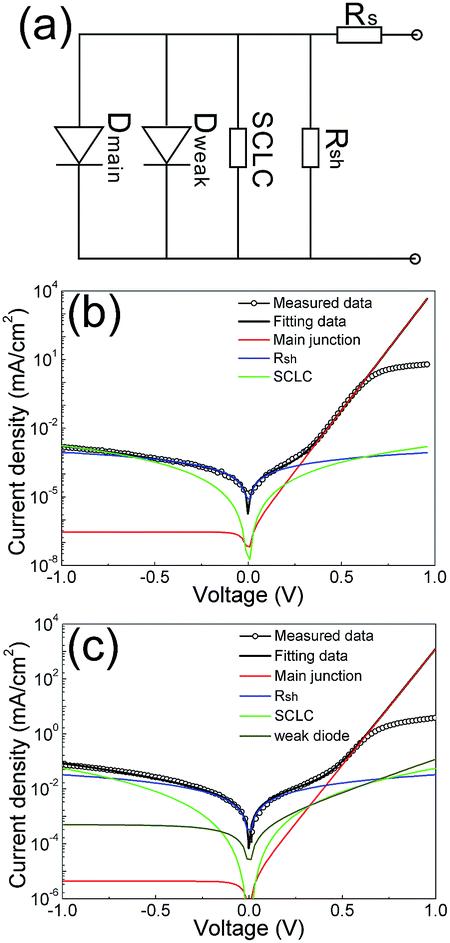 | ||
| Fig. 8 (a) Equivalent compact electric circuit model for a CdTe thin film solar cell; experimental dark current–voltage data and the fitting curves from the contributions of different shunting paths for (b) a solar cell with a through-thickness CdTe film and (c) a solar cell with a low-quality CdTe film. | ||
Fig. 8(b) and (c) show the experimental dark J–V data and the curve fittings, which accounted for the different contributions induced by the shunting paths discussed above. For the solar cell with a CdTe absorber layer prepared at the high PO2 of 0.3 kPa, see Fig. 8(b), the current shunting were mainly contributed by the SCLC and the ohmic shunting. At the voltage range of −1 to −0.5 V, the shunting contribution from the SCLC and the Rsh are in the same level, and both the currents are relatively small, with values of ∼10−6 A cm−2 at the voltage of −1.0 V. At the positive voltage range of 0.3–0.7 V, the dark current was dominated by the main junction. For the solar cell with a CdTe absorber layer prepared at the low PO2 of 0.1 kPa, at voltage higher than ∼0.5 V, comparable shunting currents induced by the ohmic shunting, the SCLC, and weak diode were observed, leading to a more or less symmetric J–V curve shape around the zero voltage, and this J–V curve shape away from that of an ideal solar cell.
The Rsh for the CdTe cell fabricated with high oxygen pressure had a value of 1.1 × 10⁶ Ω cm2, about one and half order higher than that of the cell fabricated with low oxygen pressure. The Rsh value of 1.1 × 10⁶ Ω cm2 is comparative to that of single crystal Si and Cu(In,Ga)Se2 solar cells.41 The diode ideality factors are 1.57 and 1.98 for the two cells fabricated with high and low oxygen pressures, respectively. The ideality factor of 1.57 indicates a very high quality CdS/CdTe heterojunction. The high-quality textured CdTe layer had a low density of grain boundaries, and the carrier recommendation at the grain boundary was reduced, leading to a much decreased ideality factor. The J–V data fittings showed that for a well fabricated CdTe cell device, the current shunting induced by a weak diode is not necessary to be considered in the electric circuit model.
4. Conclusions
We propose and demonstrate results in support of a vapor–liquid–solid crystalline growth mechanism for CdTe film growth by employing a close-spaced sublimation technique at the presence of high pressure oxygen. The low-melting liquid mixture on the surface of a growing CdTe grain assisted material adsorption and transport of Cd and Te2 from the vapor through the liquid to the liquid–solid interface, where they reacted and epitaxially crystallized to form CdTe on well faceted CdTe grains. CdTe solar cells fabricated with through-thickness CdTe grains showed much enhanced carrier collection efficiency and high short-circuit current of ∼25 mA cm−2. This was ascribed to the much reduced carrier recombination/scattering occurred at the grain boundaries. CdTe solar cells fabricated with through-thickness CdTe absorbers demonstrated an efficiency as high as 14–15.2%, which is much higher than that fabricated with non through-thickness grains.Acknowledgements
This work was financially supported by the National Natural Science Foundation of China (No. 51272247, 61474103) and Anhui Province Natural Science Foundation (No. 1408085MF119).Notes and references
- M. A. Green, K. Emery, Y. Hishikawa, W. Warta and E. D. Dunlop, Prog. Photovoltaics, 2012, 20, 12–20 Search PubMed.
- http://en.wikipedia.org/wiki/Solar_cell.
- Z. Bai, J. Yang and D. Wang, Appl. Phys. Lett., 2011, 99, 143502 CrossRef.
- R. Yang, D. Wang, L. Wan and D. Wang, RSC Adv., 2014, 4, 22162–22171 RSC.
- S. G. Kumar and K. S. R. K. Rao, Energy Environ. Sci., 2014, 7, 45–102 CAS.
- S. A. Ringel, A. W. Smith, M. H. MacDougal and A. Rohatgi, J. Appl. Phys., 1991, 70, 881–889 CrossRef CAS.
- J. P. Enriquez and X. Mathew, J. Mater. Sci.: Mater. Electron., 2005, 16, 617–621 CrossRef CAS.
- D. H. Rose, D. L. Rick, J. Matson, D. S. Albin, R. G. Dhere and P. Sheldon, 25th Photovoltaic Specialists Conference, 1996, pp. 777–780 Search PubMed.
- D. S. Albin, Y. Yan and M. M. Al-Jassim, Prog. Photovoltaics, 2002, 10, 309–322 CAS.
- V. Valdna, Sol. Energy Mater. Sol. Cells, 2005, 87, 369–373 CrossRef CAS.
- G. Gordillo, J. M. Flórez and L. C. Hernández, Sol. Energy Mater. Sol. Cells, 1995, 37, 273–281 CrossRef CAS.
- M. Emziane, K. Durose, D. P. Halliday, A. Bosio and N. Romeo, Appl. Phys. Lett., 2005, 87, 261901 CrossRef.
- V. D. Falcao, W. A. Pinheiro, C. L. Ferreira and L. R. O. Cruz, Mater. Res., 2006, 9, 29–32 CrossRef CAS.
- B. A. Korevaar, J. R. Cournoyer, O. Sulima, A. Yakimov and J. N. Johnson, Prog. Photovoltaics, 2014, 22, 1040–1049 CAS.
- A. L. Fahrenbruch and R. H. Bube, Fundamentals of Solar Cells: Photovoltaic Solar Energy Conversion, Academic Press, New York, USA 1983 Search PubMed.
- A. Morales-Acevedo, Sol. Energy Mater. Sol. Cells, 2006, 90, 2213–2220 CrossRef CAS.
- Z. Bai and D. Wang, Phys. Status Solidi A, 2012, 209, 1982–1987 CrossRef CAS.
- C. V. Thompson, Annu. Rev. Mater. Sci., 1990, 20, 245–268 CrossRef CAS.
- Z. Cao, Thin film growth: physics, materials science and applications, Woodhead Publishing, Philadelphia, USA 2011 Search PubMed.
- K. Nakamura, M. Gotoh, T. Fujihara, T. Toyama and H. Okamoto, Sol. Energy Mater. Sol. Cells, 2003, 75, 185–192 CrossRef CAS.
- B. Siepchen, A. Klein and W. Jaegermann, Phys. Status Solidi RRL, 2008, 2, 169–171 CrossRef CAS.
- D. Wang, Z. Hou and Z. Bai, J. Mater. Res., 2011, 26, 697–705 CrossRef CAS.
- W. Li, R. Yang and D. Wang, Sol. Energy Mater. Sol. Cells, 2014, 123, 249–254 CrossRef CAS.
- R. Schneider, C. Wolpert, H. Guilloteau, L. Balan, J. Lambert and C. Merlin, Nanotechnology, 2009, 20, 225101 CrossRef PubMed.
- S. Chun, S. Lee, Y. Jung, J. S. Bae, J. Kim and D. Kim, Curr. Appl. Phys., 2013, 13, 211–216 CrossRef.
- Z. Q. Wang and D. Stroud, Phys. Rev. B: Condens. Matter Mater. Phys., 1989, 40, 3129–3132 CrossRef CAS.
- K. Yokota, Y. Yoshimatsu, S. Katayama and T. Kariya, Jpn. J. Appl. Phys., 1979, 18, 1757–1766 CrossRef CAS.
- R. S. Wagner and W. C. Ellis, Trans. Metall. Soc. AIME, 1965, 233, 1053–1064 CAS.
- R. S. Wagner and W. C. Ellis, Appl. Phys. Lett., 1964, 4, 89–90 CrossRef CAS.
- J. Hiie, Thin Solid Films, 2003, 431–432, 90–93 CrossRef CAS.
- T. A. Mohamed, I. Shaltout and K. M. Al Yahyaei, Spectrochim. Acta, Part A, 2006, 64, 106–115 CrossRef PubMed.
- B. K. Rai, H. D. Bist, R. S. Katiyar, K. T. Chen and A. Burger, J. Appl. Phys., 1996, 80, 477–481 CrossRef CAS.
- F. Caballero-Briones, A. Zapata-Navarro, A. Martel, A. Iribarren, J. L. Peña, R. Castro-Rodríguez, P. Bartolo-Pérez, F. Rábago-Bernal and S. Jiménez-Sandoval, Superficies Vacio, 2006, 16, 38–42 Search PubMed.
- A. S. Pine and G. Dresselhaus, Phys. Rev. B: Solid State, 1972, 5, 4087–4093 CrossRef.
- J. Motohisa, J. Noborisaka, J. Takeda, M. Inari and T. Fukui, J. Cryst. Growth, 2004, 272, 180–185 CrossRef CAS.
- W. S. Shi, Y. F. Zheng, N. Wang, C. S. Lee and S. T. Lee, Appl. Phys. Lett., 2001, 78, 3304–3306 CrossRef CAS.
- X. Wu, Sol. Energy, 2004, 77, 803–814 CrossRef CAS.
- T. Toyama, T. Suzuki, M. Gotoh, K. Nakamura and H. Okamoto, Sol. Energy Mater. Sol. Cells, 2001, 67, 41–47 CrossRef CAS.
- K. Shen, Q. Li, D. Wang, R. Yang, Y. Deng, M. Jeng and D. Wang, Sol. Energy Mater. Sol. Cells, 2016, 144, 472–480 CrossRef CAS.
- S. Dongaonkar, J. D. Servaites, G. M. Ford, S. Loser, J. Moore, R. M. Gelfand, H. Mohseni, H. W. Hillhouse, R. Agrawal, M. A. Ratner, T. J. Marks, M. S. Lundstrom and M. A. Alam, J. Appl. Phys., 2010, 108, 124509 CrossRef.
- A. Virtuani, E. Lotter, M. Powalla, U. Rau and J. H. Werner, Thin Solid Films, 2004, 451–452, 160–165 CrossRef CAS.
| This journal is © The Royal Society of Chemistry 2016 |