DOI:
10.1039/C6RA05189H
(Paper)
RSC Adv., 2016,
6, 37079-37084
Silicon direct bonding via low-temperature wet chemical surface activation
Received
27th February 2016
, Accepted 1st April 2016
First published on 4th April 2016
Abstract
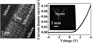
Commercial silicon substrates were bonded via low-temperature wet chemical surface activation in a standard laboratory without ultrahigh vacuum or a clean room. A smooth direct bond with no voids or microcracks was obtained, and the best bonding strength reached up to 4.15 MPa at 250 °C with the 25 MPa pressure-assisted process. The p–n junction prepared using this method exhibited excellent I–V characteristics. An updated model for the silicon direct bonding mechanism was proposed and proved. Raman scattering analysis indicated an increase in the Si–OH density on the silicon surface after the activation treatment. Cross-sectional HRTEM and EELS analysis crossing the interface indicated that the Si–O–Si linkage on the bonding interface that formed after low-temperature annealing was of a lower density than that of the native oxide. The thickness of the bonding interface decreased and the silicate linkage underwent further densification when high-temperature annealing was executed.
Introduction
Silicon is ubiquitous in the field of electronics. Since Lasky J. B.1 and Shimbo M.2 first reported on silicon direct bonding (SDB) technology in 1986, SDB has been widely used for the manufacture of silicon-on-insulator (SOI) devices, optoelectronic devices, microelectromechanical systems (MEMS) and three-dimensional (3D) level integrations. However, the conventional fusion SDB was usually performed at high temperature (∼1000 °C), which may broaden the doping profile of silicon and induce thermal or residual stress. In recent years, surface activated bonding (SAB)3 of silicon bonds has been successfully achieved by several advanced methods, such as fast atom beam (FAB),4 reactive ion etching (RIE),5 microwave (MW) radiation plasma,6,7 ultraviolet radiation plasma,8 and so on. However, these SAB processes always required rigorous conditions for sample preparation and a demanding operating environment, such as a low surface roughness (<0.5 nm) and ultrahigh vacuum (UHV) in a clean room. Furthermore, the bonding mechanism remains poorly understood.9–12
In this contribution, we developed a wet chemical surface activation method to directly bond the silicon pieces at low temperature. The p–n junction prepared using this method exhibited excellent I–V characteristics. With the aid of high resolution transmission electron microscopy (HRTEM) and electron energy loss spectroscopy (EELS) analysis, we demonstrated that excellent interfaces of the bonded silicon pairs could be obtained without rigorous conditions, and we proposed an updated model for silicon direct bonding.
Experimental section
Materials
Two types (both p-type and n-type) of (100)-oriented double-polished commercial silicon pieces (10 mm × 10 mm) provided by Shanghai Daheng Optics and Fine Mechanics Co., Ltd were used, one with the native oxide (2–4 nm) and one with a thermally grown oxide (250 nm). The thickness of the silicon pieces was approximately 500 ± 15 μm. The chemicals used in the experiments were all analytical reagents (AR) and were supplied by Sinopharm Chemical Reagent Co., Ltd including ammonia (25–28% NH4OH), hydrogen peroxide (30% H2O2), methanol (99.5% CH3OH), acetone (99.0% CH3COCH3), concentrated hydrochloric acid (36–38% HCl) and concentrated sulfuric acid (95–98% H2SO4). Deionized water (Milli-Q Reference) with a resistivity of 18.2 MΩ cm−1 was used.
Bonding procedure
The direct bonding of the silicon pieces is shown in the following. First, all samples were cleaned by a multistage ultrasonic-assisted process. The cleaning solution included acetone, methanol, a sulfuric acid (H2SO4)/hydrogen peroxide (H2O2) mixture (SPM) (H2SO4
:
H2O2 = 4
:
1), and standard RCA-1 (NH4OH
:
H2O2
:
H2O = 1
:
1
:
5) and RCA-2 (HCl
:
H2O2
:
H2O = 1
:
1
:
5). Second, the samples were then rinsed in an activation solution (NH4OH
:
H2O2
:
H2O = 6
:
1
:
3) at 80 °C for 30 min to complete the activation process. Third, the samples were carefully put into direct contact with each other under DI water, and the combined pieces were subsequently dried in a vacuum drying oven (DZF-6020) at 100 °C for 2 h to complete the pre-bonding process. Finally, pressure (5–25 MPa) was applied to the samples by a stainless steel jig. The jig was held in a vacuum drying oven and maintained at 250 °C for 2 to 10 h to complete the low-temperature annealing. Note that all these operations were performed in a standard laboratory without UHV or a clean room.
To confirm the comparably low density of the as-bonded interface, we investigated the interface behaviours of the bonded silicon pairs after high-temperature annealing. We applied 30 min of 1000 °C annealing to the as-bonded silicon samples with the native oxide (250 °C with 25 MPa pressure-assisted annealing for 10 h) in a muffle furnace (CARBOLITE® HTF1700).
Characterization
The surface roughness and surface chemistry of the samples were measured using atomic force microscopy (AFM, CSPM5500) and a Raman scattering spectrometer (Renishaw Invia Reflex), respectively. For bonding strength measurements, the bonded specimens were glued to stainless steel jigs clamped to the fixture of a pulling tester with a pulling speed of 0.05 mm min−1. For interface characterizations, cross-sectional samples of the direct bonds were examined by scanning electron microscopy (SEM), HRTEM, Z-contrast scanning TEM (STEM) and EELS. Cross-sectional TEM samples were prepared using a focused ion beam (FIB) double beam system (FEI Helios Nano Lab 600). TEM observations and EELS analyses were both performed using a Tecnai G2 F20 instrument equipped with a Gatan GIF Quantum 963 energy filter.
To minimize the radiation dose and the beam-induced carbon contamination around the bonding interface, the electron beam was rastered over a rectangular area when EEL spectra were collected. During the signal acquisition, the following conditions were applied: 0.5 eV per channel, a convergence angle of ∼18.26 mrad, a collection angle of ∼21 mrad at zero projection lens current, and an acquisition time of 0.1 s. We optimized the probe size and condenser lens aperture size to enhance the EEL spectra. According to the method described in ref. 13, we quantified all the EELS spectra using the Hartree–Slater cross section model and power-law background fitting.
For the I–V characteristics of the prepared p–n junction, conductive electrodes with a 2 mm diameter were prepared by applying silver paste at the center on both sides of the bonded specimen.
Results and discussion
Surface roughness and surface chemistry
The surface roughness of the silicon pieces (approximate 4 nm, peak–peak roughness) remained unchanged before and after the activation process (Fig. 1a and b). Before activation there were many small contaminations larger than 4 nm (white spots in Fig. 1a) on the silicon surface. These were stubborn pollutants which could not be cleaned by an acetone and methanol ultrasonic-assisted cleaning process, however, they can be cleaned off after activation. Raman spectra were collected from the activated and non-activated silicon surfaces with the native oxide (Fig. 1c). The intensities of the peaks at approximately 940 cm−1 and 980 cm−1, corresponding to Si–OH,14 increased after the activation treatment, whereas the intensity of the peak at approximately 300 cm−1, related to the Si–Si bond, slightly decreased.15 This result indicates an increase of the Si–OH density and the hydrophilicity on the silicon surface.
 |
| Fig. 1 AFM images of the silicon surface with the native oxide (a) before activation and (b) after the activation, and (c) Raman spectra collected from the non-activated and activated silicon surface with the native oxide. | |
Bonding strength
Direct bonding requires contaminant-free conditions. If any dust remains in the interface, the bonding will fail. With an appropriate bonding process (250 °C with 25 MPa pressure-assisted annealing for 10 h), we can achieve a high-quality direct bond. The bonding strength of the bonded pairs with the native oxide at low temperature was as high as 4.15 MPa, which is comparable to the wafer bonded by plasma in a clean room.16 We found that the bonding strength increased with the bonding temperature (Fig. 2a), bonding time (Fig. 2b) and pressure (Fig. 2c). The bonding temperature had the most significant effect on the bonding strength. We investigated four different bonding temperatures and we found that the bonding strength considerably increased as the bonding temperature increased from 100 to 250 °C. The effects of the bonding time and the applied pressure are minor, since the bonding strength slightly increased with the extended bonding time and reinforced pressure.
 |
| Fig. 2 The bonding strengths of samples with the native oxide prepared at different (a) annealing temperatures, (b) annealing times and (c) pressures. | |
The p–n junction fabrication
A p–n junction was prepared using this modified method by directly bonding p- and n-type silicon with the native oxide. Fig. 3a shows the I–V characteristics of the as-bonded p–n silicon conjunction, which exhibited excellent one-way electrical conduction. However, the two aligned unbonded silicon pieces showed no current density. The applied voltage was from −4 V to 4 V, and the maximum current density was 0.1 mA, which is comparable to that of a wafer bonded by plasma in a cleanroom,17 indicative of the atomic bonding. A particular C-mode scanning acoustic microscopy (C-SAM) image of the bond is presented in the inset of Fig. 3a. There is only a sporadic distribution of white spots in the bonding interface image, suggesting that the sample was bonded well. The white spots in the C-SAM image are unbonded areas, which might be caused by remaining dust and air bubbles.
 |
| Fig. 3 (a) The I–V characteristics of the p–n junction prepared through low-temperature wet chemical activation. (b) SEM image of the bonding interface of thermal oxide silicon prepared by surface activated direct bonding. The inset of (a) shows a particular C-SAM image of the silicon bond interface. | |
Interface characterizations
SEM can detect the bonding interface of the silicon pieces with a thermal oxide (250 nm) layer (Fig. 3b), but this is not applicable for the counterpart with a native oxide layer (2–4 nm thick). However, detailed interfacial behaviour could not be detected using SEM. Therefore, we performed TEM on cross-sectional samples of the as-bonded silicon pairs with the native oxide prepared using a focused ion beam (FIB).
Interfacial HRTEM showed that the bond interface of the low-temperature direct bonding silicon joint at 250 °C with 25 MPa assisted-pressure has no voids or cracks (Fig. 4a). EELS signals containing both Si-L2,3 and O-K edges were collected across the bonding interface (Fig. 4d and e) with a separation of approximately 1 nm between each spectrum as in our previous work.18 The Si-L2,3 edge shifts from 102 eV to 108 eV and then returns to 102 eV along the bonding interface because of the different energies of different Si bonds. There was a slight decrease in intensity at the middle of the interface. The O-K edge (540 eV) appears at the bonding interface and then disappears at the silicon base. The intensity of the O-K edge first increases, then decreases, and then increases again along the interface. Further details about the interface structure were obtained by quantifying the O/Si ratio around the interface. The O/Si ratio was determined based on the EELS analysis introduced in ref. 13. We found that the O/Si ratio of the low-temperature bonding exhibited a slight decrease at the middle of the interface (Fig. 4c), decreasing from 1.0 to 0.8. This is likely to be due to the generation of the SiOx transition layer and the low density at the bonding interface.13 These results confirmed the formation of the Si–O–Si linkage on the bonding interface after low-temperature annealing.
 |
| Fig. 4 (a) Interfacial HRTEM image of the as-bonded silicon pair with the native oxide; the line with a double arrow and the dashed line marked the oxide layer on silicon and interface, respectively. (b) Local STEM image of the EELS line-scan position. (c) Profile of the O/Si ratio obtained by EELS quantification. (d) Si-L2,3 and (e) O-K edges recorded along the scanning line. Dashed lines in (d) mark the positions of the Si-L2,3 edges. The red region in (e) indicated the positions of the O-K edges. Spectra obtained from left to right positions of the interface marked with numbers from negative to positive. | |
When high-temperature annealing is applied, interface evolution occurred and that confirmed the comparably low density of the as-bonded interface. We found that the bonding interface presents a thinner oxide layer (∼3 nm) from the image obtained by interfacial HRTEM as shown in Fig. 5a. EELS signals containing both Si-L2,3 and O-K edges were also collected across the bonding interface of the high-temperature annealing sample (Fig. 5d and e) with a separation of approximately 1 nm between each spectrum along the scanning line (Fig. 5b). The Si-L2,3 signal changes in the same way from 102 eV to 108 eV and then back to 102 eV again around the bonding interface according to the different energies of different Si bonds, but there is no intensity drop at the middle of the interface. From O-K edge signals, we also couldn’t find any intensity drop at the middle of bonding interface (Fig. 5e). Quantification of the O/Si ratio around the interface of the high-temperature annealing bonding exhibited no decrease at the middle of the interface (Fig. 5c), and the ratio remained stable at approximately 1.0 at the middle of the interface. These results confirmed that the low-density interface would undergo further densification when high temperature annealing was applied. However, the bonding strength of the direct bond obtained at low-temperature can satisfy the requirements for electronics applications.
 |
| Fig. 5 (a) Interfacial HRTEM image of the high-temperature annealing silicon pair with the native oxide; the line with a double arrow and the dashed line marked the oxide layer on silicon and interface, respectively. (b) Local STEM image of the EELS line-scan position. (c) Profile of the O/Si ratio obtained by EELS quantification. (d) Si-L2,3 and (e) O-K edges recorded along the scanning line. Dashed lines in (d) marked the positions of the Si-L2,3 edges. The red region in (e) indicated the positions of the O-K edges. Spectra obtained from left to right positions of the interface marked with numbers from negative to positive. | |
Bonding mechanism
Some models have been proposed for the mechanism of silicon wafer direct bonding,19–21 however, the chemical state of the active silicon surface and the interface behaviour around the bonded interface have not been well understood. We proposed a new bonding model for silicon direct bonding via wet chemical activated treatment in a standard laboratory, giving detailed information about the microstructure of the active silicon surface and the direct bonding interface. This model includes three stages: activation process, pre-bonding and annealing.
The activation process includes breakage of the silicate (Si–O–Si) linkage and formation of silanol groups (Si–OH). The crystalline silicon surface was always covered with an oxide layer. Silicon oxide (SiOx) is generally in an amorphous state. Its structure consists of [SiO4]4− tetrahedral units that are bridged by Si–O–Si linkages.22 Pristine silicon oxide surfaces contain a certain amount of Si–OH functional groups. During the activation process, Si–O–Si linkages on the silicon oxide surface are broken, and more activated groups (Si–OH) are created on the fresh surface as indicated in reaction (1). This process was supported by the Raman spectra (Fig. 1c). After surface activation, the increased intensity of Raman peaks related to Si–OH at approximately 940 cm−1 and 980 cm−1 confirmed the increased density of Si–OH on the surface of silicon oxide.
|
Si–O–Si + HOH → Si–OH + HO–Si
| (1) |
With the increase of the duration of activation, more Si–OH is attached to the silicon oxide surface. H2O molecules can also be adsorbed via hydrogen bonding. Finally, a single colloid-like, hydrolyzed layer would uniformly form on the surface as shown in Fig. 6a.23 This layer contains a high density of –OH and H2O with nanoscale thickness and lower viscosity than that of the pristine silicon oxide bulk.
 |
| Fig. 6 Schematics of the low-temperature silicon direct bonding mechanism: (a) interface of the silicon bonding pair after the pre-bonding process at 100 °C. (b) Schematic of the bonded glass pair after annealing using pressure-assisted annealing at 250 °C. The local enlarged image of (a) shows the inner surface state of the nanogap remaining in the interface. The dark area indicated the not-fully-dehydrated hydrolyzed layer. | |
During pre-bonding, face-to-face silanol groups on the contact surface will react with each other and transform into Si–O–Si linkages (reaction (2)), thus closing the interface with the concomitant removal of water.
|
Si–OH + HO–Si → Si–O–Si + HOH
| (2) |
The transformation of two adjacent silanol groups into one siloxane spontaneously occurs because it is an exothermal process.24 However, only a small degree of adhesion can be achieved after pre-bonding. Some nanogaps were still present in the interface, and the inner surface of these nanogaps continued to retain unbound silanol groups (Fig. 6a), because further transformation becomes endothermic due to the spatial restrictions from the adjacent siloxane bonds. To strengthen the silicon joint, additional energy is required to close all these nanogaps.24 Applied pressure can overcome the geometric constraints, but this requires a certain temperature, otherwise these nanogaps will not close. This also explains why the annealing temperature is the most influential factor (Fig. 2a).
When a pre-set pressure was applied during the 250 °C annealing, a dehydration–condensation process occurred. This process was similar to the inverse process of stress corrosion.25 According to the local deformation of the hydrolyzed layer, the remaining silanol groups reacted with the adjacent groups and the nanogaps were closed. Simultaneously, the produced water slowly diffused away through the interface or diffused into the silicon oxide bulk. When the dehydration–condensation process of the interface was completed, a smooth bonded joint was obtained (Fig. 6b). The network density of the newly formed interface might be lower than that of the silicon oxide on the silicon surface, which coincides with the O/Si ratio profile in Fig. 4c.
If high temperature annealing was applied, the newly formed interface might undergo further condensation until the whole oxide homogenized, and the bonding interface width decreased (Fig. 5a).
Conclusions
In summary, we directly bonded silicon substrates using wet chemical surface activation at a low temperature in a standard laboratory without UHV or a clean room. The bonding strength reached as high as 4.15 MPa at 250 °C. The p–n junction prepared using this method exhibited I–V characteristics of forward conduction performance, thus confirming the atomic bonding of the silicon. The silicon oxide and the uniform hydrolyzed layer formed on the silicon surface after the wet chemical surface activation play important roles in the bonding process. The linkage of the newly formed interface at low-temperature was softer than that of the pristine silicon oxide bulk, and it underwent further densification when high-temperature annealing was executed. However, the bonding strength obtained at a low-temperature can satisfy the requirements for electronics applications.
Acknowledgements
This research was supported by Grant 201509030004 from Guangzhou Science and Technology Plan Project. Prof. He Kejian and Dr Yan Ning at Central South University are greatly appreciated for their assistance of EELS analysis. Associate professor Lv Shilong at Shanghai Institute of Microsystem and Information Technology is acknowledged for his support in preparation of the TEM sample.
Notes and references
- J. B. Lasky, Appl. Phys. Lett., 1986, 48, 78 CrossRef CAS.
- M. Shimbo, K. Furukawa, K. Fukuda and K. Tanzawa, J. Appl. Phys., 1986, 60, 2987 CrossRef CAS.
- R. Kondou, C. Wang, A. Shigetou and T. Suga, Microelectron. Reliab., 2012, 52, 342 CrossRef CAS.
- Y. Kurashima, A. Maeda and H. Takagi, Microelectron. Eng., 2014, 118, 1 CrossRef CAS.
- C. Wang and T. Suga, Microelectron. Reliab., 2012, 52, 347 CrossRef CAS.
- H. Moriceau, F. Rieutord, F. Fournel, L. Di Cioccio, C. Moulet, L. Libralesso, P. Gueguen, R. Taibi and C. Deguet, Microelectron. Reliab., 2012, 52, 331 CrossRef CAS.
- C. Wang and T. Suga, J. Electrochem. Soc., 2011, 158, H525 CrossRef CAS.
- Y. Xu, C. Wang, Y. Dong, L. Li, K. Jang, K. Mawatari, T. Suga and T. Kitamori, Anal. Bioanal. Chem., 2012, 402, 1011 CrossRef CAS PubMed.
- M. M. Howlader, G. Kagami, S. H. Lee, J. G. Wang, M. Kim and A. Yamauchi, J. Microelectromech. Syst., 2010, 19, 840 CrossRef CAS.
- C. M. Tan, W. Yu and J. Wei, Appl. Phys. Lett., 2006, 88, 114102 CrossRef.
- C. Ventosa, F. Rieutord, L. Libralesso, C. Morales, F. Fournel and H. Moriceau, J. Appl. Phys., 2008, 104, 123524 CrossRef.
- T. Plach, K. Hingerl, S. Tollabimazraehno, G. Hesser, V. Dragoi and M. Wimplinger, J. Appl. Phys., 2013, 113, 094905 CrossRef.
- T. Zheleva, A. Lelis, G. Duscher, F. Liu, I. Levin and M. Das, Appl. Phys. Lett., 2008, 93, 022108 CrossRef.
- S. Agnello, D. Di Francesca, A. Alessi, G. Iovino, M. Cannas, S. Girard, A. Boukenter and Y. Ouerdane, J. Appl. Phys., 2013, 114, 104305 CrossRef.
- P. A. Temple and C. E. Hathaway, Phys. Rev. B: Condens. Matter Mater. Phys., 1973, 7, 3685 CrossRef CAS.
- M. M. R. Howlader, T. Suga, H. Itoh, T. H. Lee and M. J. Kim, J. Electrochem. Soc., 2009, 156, H846 CrossRef CAS.
- M. M. R. Howlader and F. Zhang, Thin Solid Films, 2010, 519, 804 CrossRef CAS.
- C. Mai, M. Li and S. Yang, RSC Adv., 2015, 5, 42721 RSC.
- Q. Tong and U. M. Gösele, Adv. Mater., 1999, 11, 1409 CrossRef CAS.
- C. Ventosa, C. Morales, L. Libralesso, F. Fournel, A. M. Papon, D. Lafond, H. Moriceau, J. D. Penot and F. Rieutord, Electrochem. Solid-State Lett., 2009, 12, H373 CrossRef CAS.
- Y. Backlund, K. Ljungberg and A. Soderbarg, J. Micromech. Microeng., 1992, 2, 158 CrossRef.
- P. F. McMillan, B. T. Poe, P. Gillet and B. Reynard, Geochim. Cosmochim. Acta, 1994, 58, 3653 CrossRef CAS.
- C. A. Murray and T. J. Greytak, J. Chem. Phys., 1979, 71, 3355 CrossRef CAS.
- O. Lichtenberger and J. Woltersdorf, Mater. Chem. Phys., 1996, 44, 222 CrossRef CAS.
- T. A. Michalske and S. W. Freiman, J. Am. Ceram. Soc., 1983, 66, 284 CrossRef CAS.
|
This journal is © The Royal Society of Chemistry 2016 |
Click here to see how this site uses Cookies. View our privacy policy here.