3D TiO2/ZnO composite nanospheres as an excellent electron transport anode for efficient dye-sensitized solar cells

Pengfei Chenga, Yinglin Wang*b, Luping Xu*a, Peng Sunb, Zisheng Suc, Fangming Jinc, Fengmin Liub, Yanfeng Sunb and Geyu Lu*b
aSchool of Aerospace Science and Technology, Xidian University, Xi'an 710126, P. R China. E-mail: lpxu@xidian.edu.cn; Fax: +86 29 81891034; Tel: +86 431 81891035
bState Key Laboratory on Integrated Optoelectronics, College of Electronic Science and Engineering, Jilin University, Changchun 130012, People's Republic of China. E-mail: lugy@jlu.edu.cn; Fax: +86 431 85167808; Tel: +86 431 85167808
cKey Laboratory of Luminescence and Application, Changchun Institute of Optics, Fine Mechanics and Physics, Chinese Academy Sciences, Changchun 130033, P. R China. E-mail: suzs@ciomp.ac.cn; Fax: +86 431 86176345; Tel: +86 431 86176345

Received 14th February 2016 , Accepted 11th May 2016

First published on 12th May 2016


Abstract

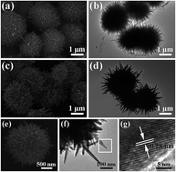
The present study aimed to develop a high electron lifetime (τr) and low transit time (τd) photoanode material for dye sensitized solar cells (DSSCs). An innovative material structure, a TiO2/ZnO composite oxide hierarchical nanosphere, was synthesized by a two-step facile hydrothermal method. This composite oxide comprised 3D urchin-like TiO2 nanospheres and 1D ZnO nanospindles (ULTZ). The ZnO nanospindles were assembled onto the surface of the 3D urchin-like TiO2 in the hydrothermal process second step. A series of ULTZs made with different growth times were characterized by X-ray diffraction (XRD), scanning electron microscopy (SEM) and transmission electron microscopy (TEM). The DSSCs based on the ULTZs exhibited much higher photoelectric properties and the energy conversion efficiency was 8.78%, which indicated a 30% increase in the conversion efficiency compared to those of the P25 electrode (6.79%); the great improvements of photoelectric properties and energy conversion efficiency for ULTZs based DSSCs were mainly attributed to the superior electronic transmission characteristics.


1. Introduction

Dye-sensitized solar cells (DSSCs) have been studied extensively since their discovery in 1991 due to their high energy-conversion efficiency and their low production cost as cheaper alternatives to silicon solar cells.1–5 DSSC is a photochemical cell composed of photoanode, dye, electrolyte and counter electrode.6–8 Apart from the search for more efficient and stable components, the morphology of photoanode materials and modification of photoanode structures have also attracted great attention.9–13 Currently, numerous efforts have been devoted to develop high performance of DSSCs. In general, high specific surface area, fast electron transport, and pronounced light-scattering effects are indispensable to a high performance photoanode.

Conventional DSSCs are fabricated using mesoporous TiO2 nanoparticle and hierarchical micron/submicron spheres photoanode,14,15 which have excellent light scattering and dye absorption abilities resulting in a high conversion efficiency. However, a major drawback of the conventional TiO2 nanoparticle or hierarchical sphere photoanode in DSSCs is the inefficient electron transport, which imposes an upper limit on the film thickness. In a film composed of anatase TiO2 nanoparticles, the electron diffusion coefficient is more than two orders of magnitude lower than that in single crystal TiO2.16,17 Therefore, the method to efficiently transfer electrons and reduce their recombination with redox species is believed to be the key step in achieving high efficiency DSSCs using TiO2 nanoparticles and micron or submicron hierarchical sphere films.

Films were fabricated from one-dimensional (1D) nanostructures can provide a direct pathway for electron transfer and has proven to be an effective way to facilitate electron transport.18–24 Using nanorods or nanotubes, the electron lifetime in photoanode films can be improved three-fold in single nanoparticle films.25 For instance, Law et al. found the electron diffusion coefficient of ZnO nanowires to be several hundred times higher than that of ZnO or TiO2 nanoparticle films.26 However, the combination photoanodes of TiO2 nanoparticles and ZnO nanowires for DSSC was investigated by Bai et al.27 This photoanode combination lacked the ability to scatter incident light. Even so, the overall power conversion efficiency reached as high as 8.44%.

As mentioned above, large surface area, high charge transfer efficiency and prominent light scattering ability are all essential properties to form an excellent performance photoanode.28–30 Liao et al.31 have presented tri-functional hierarchical pure TiO2 spheres for DSSCs, but a composite oxide combining these three beneficial functions was rarely reported. We know that a combination of TiO2 and ZnO nanostructures could improve the DSSC performance. This is mainly due to improved stability and increased recombination rate suppression by introducing the TiO2 to passivate the recombination sites compared with a pure ZnO photoanode. Enhanced electron transport ability can be increased by introducing ZnO to obtain faster electron transport and longer electron lifetime compared with a pure TiO2 photoanode. Herein, we report an innovative material structure for use as DSSCs photoanodes. A TiO2/ZnO composite oxide hierarchical nanosphere was synthesized through a two-step facile hydrothermal method. This composite oxide comprised 3D urchin-like TiO2 nanospheres and 1D ZnO nanospindles (ULTZ). The ZnO nanospindles were assembled on the surface of the 3D urchin-like TiO2. To reveal how this material (TiO2/ZnO composite) impacted their photoelectric properties, the as-synthesized ULTZ was used as a DSSC photoanodes.

In our previous study, the DSSCs were fabricated with trilaminar layer photoanodes and exhibited the highest photoelectric conversion efficiency (8.80%). However, the photoelectric conversion efficiency of general and conventional double layer photoanode DSSCs (ULTZ as top layer) achieved 8.78% in this study. Indeed, compared to the cells that were fabricated with a single layer (pure P25 TiO2) photoanode and trilaminar layer photoanode, the DSSCs based on the as-prepared ULTZ improved upon the photoelectric performance greatly. In this study, we use conventional double layer photoanode DSSCs ZnO and TiO2 as examples of how the composite ratio affects the DSSCs photoelectric properties.

2. Experimental details

2.1 Materials synthesis

Preparation of ZnO–TiO2 (ULTZ) composites: the 3D urchin-like TiO2 nanospheres and 1D ZnO nanospindles (ULTZ) were grown through a two step hydrothermal growth processes. In the first step 3D urchin-like TiO2 was synthesized according to a procedure based on our previously published report.32 The second step involved generating 1D ZnO nanospindles/nanorods. 100 mg urchin-like TiO2 spheres (the products of the first step), 2.5 mg Zn(NO3)2·6H2O and 5 mL of 0.05 mol L−1 hexamethylenetetramine (HMT, C6H12N4) solution were added to 30 mL deionized water, the solution was stirred gently for 10 min. Then, the homogeneous solution was transferred into a stainless Teflon-lined 50 mL autoclave and the autoclave was sealed and heated at 100 °C for 1–5 h. The system was then allowed to cool to ambient temperature and the white products were collected and washed with ethanol and deionized water several times and then dried in an oven at 60 °C.

2.2 Fabrication and measurements of DSSCs

To prepare the DSSC working electrodes, hydroxypropyl cellulose (Aldrich) was added to diethylene glycol with a ∼10 wt% concentration. The paste was added into the stock P25 TiO2 colloids wet product (containing ∼15% net TiO2) in a proportion of ∼40 wt% of P25 TiO2 weight. The mixture was vigorously stirred for about 2 h to obtain the slurry for the semi-transparent adsorption layer. The paste was also added into the obtained ULTZ product with a ∼40 wt% TiO2 ratio. After stirring, the slurry for the scattering layer was prepared. The bilayer film was constructed by the doctor-blade method through two-step calcination. Nanocrystals were spread onto fluorine-doped tin oxide (FTO) glass substrate (resistivity 14 Ω square−1, Nippon Sheet Glass, Japan) with adhesive tape to control the film thickness. After drying at 125 °C for 6 min, another layer of ULTZ was deposited on the semi-transparent layer and the electrodes coated with the TiO2 pastes were gradually heated under an airflow at 325 °C for 5 min, at 375 °C for 5 min, at 450 °C for 15 min, and finally, at 500 °C for 15 min.33 After cooling to 80 °C, the thick film with a double-layer structure was loaded with dye by immersing it in a 0.5 mM Ru-dye (cis-dithiocyanate-N,N′-bis-(4-carboxylate-4-tetrabutyl ammoniumcarboxylate-2,2′-bipyridine) ruthenium(II) (N719, Solaronix SA, Switzerland) for 24 h at room temperature. The resulting films using a double layer structure were then sandwiched together with platinized FTO counter electrodes and the electrolyte was then injected into the cell from the edges by a capillary. The electrolyte content was 0.05 M LiI, 0.05 M I2, 0.5 M 4-tert-butylpyridine (Aldrich) and 0.6 M 1-propyl-3-methylimidazolium iodide (PMII) in 3-methoxypropionitrile. The working electrode film area for the solar cell performance test was a representative 0.25 cm2.

2.3 DSSC performance measurement

The current–voltage (IV) characteristics were measured with a Keithley 2400 Source Meter under one sun AM 1.5 G (100 mW cm−2) illumination with a solar light simulator (Newport, Model: 94023A). A 450 W xenon arc lamp (Newport, Model: 6280NS) served as the light source and its incident light intensity was calibrated with a NREL-calibrated Si solar cell equipped with a optical filter to approximately AM 1.5 G one sun light intensity before each measurement. The incident photon to current efficiency (IPCE) spectra was measured as a function of wavelength from 350 to 800 nm with a 5 nm spectral resolution on the basis of a Spectral Product Zolix DSC300PA. Intensity-modulated photovoltage spectroscopy (IMVS) and intensity-modulated photocurrent spectroscopy (IMPS) measurements were carried out on an electron lifetime and dispersion test system (PSL-100) with a diode laser light source with variable intensities at 620 nm. The EIS experiments were performed using an electrochemical workstation (Solartron SI1287) at a −0.8 V bias potential.

2.4 Characterizations of ULTZ

The crystal structure of the as-prepared ULTZ was investigated by X-ray diffraction (XRD) (Rigaku TTRIII, with Cu Kα1 radiation). The morphology and microstructure were examined with a field-emission scanning electron microscope (FESEM, JEOL JSM-7500F, operating at a 15 kV acceleration voltage). Transmission electron microscopy (TEM) measurements were obtained on a JEOL JEM-2100 microscope operating at 200 kV. The specific surface area was measured using the Brunauer–Emmett–Teller (BET) equation based on the nitrogen adsorption isotherm obtained with a Micromeritics Gemini VII apparatus (surface area and porosity system).

3. Results and discussion

3.1 Structure and morphology

The detailed morphology and structural features of the product samples were observed by scanning electron microscopy (SEM) and transmission electron microscopy (TEM). Fig. 1a and b display the SEM and TEM images of the first step hydrothermal growth of pure TiO2 products; this is our previous study on urchin-like TiO2 spheres. The microspheres are composed by serried thorns, and the dense thorns form a lot of plicated ribbon on the surface of microspheres. As shown in Fig. 1c and d, the urchin-like TiO2 spheres are uniformly coated by ZnO nanospindles after the second hydrothermal growth process (products are named ULTZ). It could be observed that the ULTZ were still monodisperse and the diameter range was from 1.5 μm to 2.5 μm. More details can be observed in Fig. 1e and f, which demonstrate the accurate detailed size of the ULTZ and the ZnO nanospindles, respectively. It reveals obviously that the spindle-like ZnO cover in the urchin-like TiO2 surface very loose and uniform. ZnO nanospindles have a biggish draw ratio and the length range was from 0.5 μm to 1 μm. Panel g in Fig. 1 is the HRTEM images of the as-prepared samples, wherein the spindle structure is further exhibited. A highly crystallized structure and the inter-plane spacings of 0.28 nm, which imply that the ZnO spindle is growing along the {100} facets, is indicated.
image file: c6ra04022e-f1.tif
Fig. 1 (a and b) SEM and TEM images of the first step hydrothermal products (urchin-like TiO2 spheres), (c–f) SEM and TEM images of the second step hydrothermal products-ULTZ, (g) HRTEM images of the as-prepared ULTZ.

3.2 Growth process and mechanism

Time-dependent experiments were carried out to shed light on the process of the second hydrothermal growth. The precipitates collected at different time intervals were characterized by SEM, which is shown in Fig. 2.
image file: c6ra04022e-f2.tif
Fig. 2 (a–d) SEM images of the products under different reaction time (named S1, S2, S3, S4, respectively), (e) schematic diagram of nanostructure growth mechanism.

Fig. 2a shows the products of first step hydrothermal, urchin-like TiO2 spheres. After the complex precursor was introduced into the hydrothermal system and maintained at 100 °C for 1 h, it can be observed that the surface of the urchin-like TiO2 spheres appeared to be embossed with ZnO, which looked like nano-tentacles (Fig. 2b). As the hydrothermal process was prolonged to 3 h, the ZnO nano-tentacles continued germinating on the surface of the urchin-like TiO2 spheres and formed nanospindles (Fig. 2c). With further prolongation of reaction time (5 h), the urchin-like TiO2 spheres were covered by ZnO compact nanorods through the assembly of the nanospindles (Fig. 2d). On the basis of the abovementioned results, a growth mechanism of the products was tentatively proposed (see Fig. 2e) to indicate the morphology evolution in the hydrothermal synthesis.

The X-ray diffraction (XRD) pattern of the samples prepared by the two step hydrothermal method is shown in Fig. 3a.


image file: c6ra04022e-f3.tif
Fig. 3 (a) XRD patterns and (b) nitrogen sorption isotherms of the as-prepared ULTZ samples. The inset illustrates the simulation diagram of PTZ3.

The well-defined and sharp Bragg peaks with high intensity indicated good sample crystallinity. As can be observed from the XRD pattern, all the diffraction peaks for the first step hydrothermal products match well with those of standard XRD patterns of anatase TiO2 (JCPDS no. 21-1272, Fig. 3a-S1). The XRD patterns of S2, S3, S4 revealed that the second step products include hexagonal wurtzite-type ZnO (JCPDS no. 79-206) and the peaks of ZnO are higher and higher with the increase of complex amount of ZnO. Moreover, no other impurity peaks were detected.

The specific surface areas of the three calcined ULTZ samples were characterized using the nitrogen gas sorption technique and typical isotherms are shown in Fig. 3b. For the sample S1, the adsorption–desorption isotherms are typical type IV with a sharp capillary condensation step and the specific surface area was 392 m2 g−1. This result was reported in previous study.32 With the second hydrothermal reaction step started and further hydrothermal reaction time prolongations, type IV isotherms with a sharp capillary condensation step still at high relative pressures, and the S2, S3 and S4 specific surface area were calculated to be 348.8, 187.3 and 122.2 m2 g−1 by the Brunauer–Emmett–Teller (BET) method. Fig. 3b inset shows the pore size distributions of these three samples. These specific surface areas and pore size distributions are still beneficial for DSSC dye absorption.

3.3 DSSCs photovoltaic performance

For comparison, four types of films with similar 15 μm thicknesses were formed onto the FTO glass with the doctor blade method. Film-1 was the single P25 layer photoanode film. Moreover, film-2, film-3 and film-4 were double-layer photoanodes, the top layers are different for each of them, and different TiO2/ZnO composite ratio hierarchical nanospheres were used for the top layers (S1, S2, and S3, 7.5 μm P25 + 7.5 μm S1, S2, S3, respectively). These four photoanodes were named P25, PTZ1, PTZ2 and PTZ3. The schematic of double layer photoanode is shown in Fig. 4 (inset).
image file: c6ra04022e-f4.tif
Fig. 4 JV curves of the DSSCs based on different photoanodes measured under one sun illumination (AM 1.5G, 100 mW cm−2). image file: c6ra04022e-u1.tif P25, image file: c6ra04022e-u2.tif PTZ1, image file: c6ra04022e-u3.tif PTZ2 and image file: c6ra04022e-u4.tif PTZ3.

After dye loading, the photocurrent density voltage (JV) curves of DSSCs based on the four films (P25: film-1, PTZ1: film-2, PTZ2: film-3 and PTZ3: film-4) were measured and the results are shown in Fig. 4. The corresponding photovoltaic parameters are summarized in Table 1. As shown in Fig. 4 and Table 1, the short-circuit current density (Jsc) of photoanode P25 was around 14.63 mA cm−2, open-circuit voltage (Voc = 0.749 V) and fill factor (FF = 0.62), the cell based on photoanode P25 showed a 6.79% efficiency (η). However, all the key parameters of DSSCs based on TiO2/ZnO composite photoanodes sample PTZ1 improved (Jsc = 15.32 cm−2; Voc = 0.760 V; FF = 0.65), which resulted in a 7.57% enhanced overall conversion efficiency (η). The PTZ2 performance was further improved with an 8.78% η. The higher Voc of the TiO2/ZnO composite photoanodes cells can be explained as a consequence of reduced recombination due to the excellent electron transport properties of the inner nanospindles network, which results in an electron density increase in TiO2 and thus the Fermi level shifts.34 According to reports, the electron lifetime in a TiO2 nanotube film is three times longer than that in a TiO2 nanoparticle film. The electrical conductivity of ZnO nanospindles/nanorods was more superior to conventional photoanode semiconductor materials (TiO2 nanoparticles), therefore, the electron lifetime improvement in the is attributed to a reduced recombination between photoanode semiconductor materials and the electrolyte.35

Table 1 Photovoltaic data of four different TiO2 films, measured under AM 1.5G one sun illumination (100 mW cm−2) and simulative resistance value (Rs, R1 and R2) from EIS spectra calculated by equivalent circuit, as shown in Fig. 7. Jsc: short-circuit photocurrent density. Voc: open-circuit photovoltage; η: total power conversion efficiency; FF: fill factora
Sample Jsc (mA cm−2) Voc (V) FF (%) η (%) Rs (Ω) R1 (Ω) R2 (Ω) Dye adsorbed (×10−7 mol cm−2)
a From IV measurements, EIS spectra and UV-Vis adsorption.
P25 14.63 0.749 0.62 6.79 14.1 6.1 64.8 0.96
PTZ1 15.32 0.760 0.65 7.57 13.8 5.7 73.2 1.78
PTZ2 15.91 0.766 0.72 8.78 13.5 5.4 91.1 1.49
PTZ3 13.24 0.775 0.72 7.39 13.7 5.5 97.5 1.15


As discussed above, ZnO nanospindles in the double layer films could provide direct pathways for electrons transfer. Moreover, the light scattering effect of the TiO2/ZnO composite hierarchical nanospheres favor enhanced light-harvesting efficiency by increasing the optical length serving as light-scattering centers (Fig. S1, ESI) and thereby enhances Jsc for the cell with the double layer films.12–15 The faster electron diffusion rate36,37 in the TiO2/ZnO composite film can be considered as the reason for the higher FF, as compared with the photoanode using bare TiO2 film.

It is noteworthy that the DSSC made of PTZ3 composite film showed a higher Voc but decreased Jsc and η. This conceivable could be caused by two reasons: one is the much lower dye loading in this PTZ3 film due to the decreased dye absorbable surface area (Table 1). Another possible reason is the reduction of the electron injection efficiency to the semiconductor electrode, for the shift of the conduction band of the electrode in the presence of more and more dense ZnO nanospindles/nanorods.38 Thus, it is very important to adjust and control the appropriate amount of ZnO nanospindles/nanorods in the films, which can facilitate electron transport and light harvesting, and eventually to improve the overall DSSC conversion efficiency.

The schematic of the electron transfer mechanism in the present DSSC is given in Scheme 1. In bare TiO2 nanoparticles based DSSCs (Scheme 1a), there may the possibility for either recombination of the injected electron at the conduction band of the TiO2 semiconductor and oxidized dye or recombination between the injected electron and tri-iodide in the redox electrolyte. However, the difference in ZnO and TiO2 energy levels reduced the recombination process (Scheme 1b). The ZnO nanospindles/nanorods facilitated rapid transport of photo generated electrons to the TiO2 conduction band. The composite film helps for easy electron transfer towards the conducting glass plate. Therefore, the overall DSSC conversion efficiency of TiO2/ZnO composite films was higher than a bare TiO2 film.


image file: c6ra04022e-s1.tif
Scheme 1 Schematic of the electron transfer mechanism in (a) TiO2 and (b) TiO2/ZnO electrodes.

Fig. 5 shows incident photon to current efficiency (IPCE) spectra for the four types of DSSCs. It can be observed that for all DSSCs the IPCE maximum appeared at 525 nm (the peak of the N719 adsorption). Among them, cell P25 had the lowest IPCE value of the DSSCs, which was explicably mainly TiO2 nanocrystals having the low specific surface area and poor light scattering property. As a reference, cells PTZ1 and PTZ3 had better IPCE values, on the basis of their diffuse reflectance spectra and specific surface area results. Similar to the IV curve trend, the IPCE values of PTZ1 was a little higher than PTZ3. It can be noted that the cell PTZ2 revealed the highest IPCE values over the whole spectral region, which can be ascribed to the appropriate TiO2/ZnO composite ratio that facilitated electron transport in the film. Moreover, rather strong light scattering and light harvesting abilities also contributed to the high IPCE values of PTZ2.


image file: c6ra04022e-f5.tif
Fig. 5 Incident photon to current conversion efficiency (IPCE) curves of the TiO2 electrodes prepared from four TiO2 samples. image file: c6ra04022e-u5.tif P25, image file: c6ra04022e-u6.tif PTZ1, image file: c6ra04022e-u7.tif PTZ2 and image file: c6ra04022e-u8.tif PTZ3.

Intensity modulation photovoltage spectroscopy (IMVS) and intensity modulation photocurrent spectroscopy (IMPS) measurements were further conducted to examine the electron lifetimes (τr) and transit times (τd) for the three DSSCs, respectively, where τr represents the recombination time of electrons in the electrolyte, while τd represents the transit time of the photogenerated electron within the photoanode films, which can be calculated by IMPS and IMVS plots using the expressions τd = 1/2πfd and τr = 1/2πfr, in which fd and fr stand for the characteristic minimum frequency of the IMPS and IMVS imaginary components, respectively.39 As shown in Fig. 6, the DSSCs with TiO2/ZnO composite photoanodes have higher τr and lower τd than the bare TiO2 based DSSCs (cell-1, P25), indicating a faster transport rate and a slower recombination rate for the TiO2/ZnO composite photoanodes. We know that in DSSCs, the grain boundary effect plays a key role and the introduction of ZnO nanospindles/nanorods would prolong the charge-transport pathway. Therefore, we can conclude that the ZnO nanospindles/nanorods in TiO2/ZnO composite photoanodes have a lower energy barrier for electron transfer through the interface than a bare TiO2 photoanode.


image file: c6ra04022e-f6.tif
Fig. 6 Light intensity dependence of the electron transit times and lifetimes in photoanodes of the four DSSCs obtained from intensity modulated measurements. image file: c6ra04022e-u9.tif P25, image file: c6ra04022e-u10.tif PTZ1, image file: c6ra04022e-u11.tif PTZ2 and image file: c6ra04022e-u12.tif PTZ3.

The electrochemical impedance spectroscopy (EIS) analysis of these four DSSCs were measured in the dark under a forward −0.8 V bias.40,41 As shown in Fig. 7, two semicircles were observed in the Nyquist plots. The smaller and larger semicircles in the Nyquist plots are attributed to the charge transfer at the counter electrode/electrolyte interface and the TiO2–ZnO/dye/electrolyte interface, respectively. The sheet resistance (Rs) of substrate, charge transfer resistance of the counter electrode (R1) and recombination resistance (R2) were analyzed by Z-view software using an equivalent circuit containing a constant phase element (CPE) and resistances (R)42 (Fig. 7, inset). As shown in Fig. 7 and depicted in Table 1, the cells based on these four photoanode structure devices revealed similar Rs and R1 of 13.8 ± 0.3 and 5.7 ± 0.4 Ω, respectively, due to the use of the same counter electrode (Pt/FTO glass) and electrolyte. However, with the increase of the ZnO content, the recombination resistance (R2) also gradually increased; the R2 values for the four devices were 64.8, 73.2, 91.1 and 97.5 Ω. This is consistent with the trend the four cells lifetimes, indicating that the TiO2/ZnO composite photoanodes had a slower electron recombination process.


image file: c6ra04022e-f7.tif
Fig. 7 Nyquist plots from electrochemical impedance spectra of the four films measured in the dark at −0.8 V bias. The inset illustrates the equivalent circuit simulated to fit the impedance spectrum.

4. Conclusions

In summary, different composite ratios TiO2/ZnO hybrid nanospheres were synthesized by a two-step hydrothermal method. The novel ULTZs were used in a conventional double layer photoanode (top layer). Due to superior electronic transmission characteristics of ULTZs, the DSSCs contained ULTZs revealed great improvements of photoelectric properties and energy conversion efficiency. Among them, PTZ1 obtained the highest power conversion efficiency (8.78%), which indicated a 30% increase in the conversion efficiency compared to those of single layer (pure P25 TiO2, 6.79%). This study indicated that the TiO2/ZnO composite materials were beneficial for enhanced electron transport ability of the DSSCs.

Acknowledgements

This work was supported by the National Nature Science Foundation of China (61172138, 61401340, 61304242, 61327804, 61520106003, 61377058 and 61374218), National High-Tech Research and Development Program of China (863 Program, No. 2014AA06A505), Science and Technology Development Program of Jilin Province (No. 20150520091JH), China Postdoctoral Science Foundation (No. 2015M572524) and the Fundamental Research Funds for the Central Universities (No. JB151304, XJS14070), Natural Science Basic Research Foundation of Shaanxi Province (No. 2016JQ6025).

Notes and references

  1. B. O'Regan and M. Grätzel, Nature, 1991, 353, 737 CrossRef.
  2. T. W. Hamann, R. A. Jensen, A. B. F. Martinson, H. V. Ryswyk and J. T. Hupp, Energy Environ. Sci., 2008, 1, 66 CAS.
  3. F. T. Kong, S. Y. Dai and K. J. Wang, Adv. OptoElectron., 2007, 13, 75384 Search PubMed.
  4. T. Prakash, Electron. Mater. Lett., 2012, 8, 231 CrossRef CAS.
  5. P. Huh and S. C. Kim, Electron. Mater. Lett., 2012, 8, 131 CrossRef CAS.
  6. P. Docampo, S. Guldin, M. Stek, P. Tiwana, M. C. Orilall, S. Huttner, H. Sai, U. Wiesner, U. Steiner and H. J. Snaith, Adv. Funct. Mater., 2010, 20, 1787 CrossRef CAS.
  7. D. B. Kuang, C. Klein, S. Ito, J. E. Moser, R. Humphry-Baker, N. Evans, F. Duriaux, C. Grätzel, S. M. Zakeeruddin and M. Grätzel, Adv. Mater., 2007, 19, 1133 CrossRef CAS.
  8. G. K. Mor, K. Shankar, M. Paulose, O. K. Varghese and C. A. Grimes, Nano Lett., 2006, 6, 215 CrossRef CAS PubMed.
  9. F. W. Zhuge, J. J. Qiu, X. M. Li, X. D. Gao, X. Y. Gan and W. D. Yu, Adv. Mater, 2011, 23, 1330 CrossRef CAS PubMed.
  10. J. Z. Chen, Y. C. Yen, W. Y. Ko, C. Y. Cheng and K. J. Lin, Adv. Mater., 2011, 23, 3970 CrossRef CAS PubMed.
  11. J. F. Qian, P. Liu, Y. Xiao, Y. Jiang, Y. L. Cao, X. P. Ai and H. X. Yang, Adv. Mater., 2009, 21, 3663 CrossRef CAS.
  12. D. P. Wu, F. Zhu, J. M. Li, H. Dong, Q. Li, K. Jiang and D. S. Xu, J. Mater. Chem., 2012, 22, 11665 RSC.
  13. P. F. Cheng, Y. X. Cai, S. S. Du, P. Sun, G. Y. Lu, J. Zheng and F. M. Liu, RSC Adv., 2013, 3, 23389 RSC.
  14. M. Grätzel, Nature, 2001, 414, 338 CrossRef PubMed.
  15. P. F. Cheng, P. Sun, S. S. Du, Y. X. Cai, X. W. Li, Z. Y. Wang, F. M. Liu, J. Zheng and G. Y. Lu, RSC Adv., 2014, 4, 23396 RSC.
  16. L. Forro, O. Chauvet, D. Emin, L. Zuppiroli, H. Berger and F. Levy, J. Appl. Phys., 1994, 75, 633 CrossRef CAS.
  17. Y. Bai, H. Yu, Z. Li, R. Amal, G. Q. Lu and L. Z. Wang, Adv. Mater., 2012, 24, 5850 CrossRef CAS PubMed.
  18. M. Adachi, Y. Murat, J. Takao, J. T. Jiu, M. Sakamoto and F. M. Wang, J. Am. Chem. Soc., 2004, 126, 14943 CrossRef CAS PubMed.
  19. M. Law, J. Goldberger and P. D. Yang, Annu. Rev. Mater. Res., 2004, 34, 83 CrossRef CAS.
  20. K. H. Yu and J. H. Chen, Nanoscale Res. Lett., 2009, 4, 1 CrossRef CAS.
  21. D. K. P. Wong, C. H. Ku, Y. R. Chen, G. R. Chen and J. J. Wu, Phys. Chem. Chem. Phys., 2009, 10, 2698 CAS.
  22. K. S. Leschkies, R. Divakar, J. Basu, E. Enache-Pommer, J. E. Boercker, C. B. Carter, U. R. Kortshagen, D. J. Norris and E. S. Aydil, Nano Lett., 2007, 7, 1793 CrossRef CAS PubMed.
  23. M. Seol, H. Kim, Y. Tak and K. Yong, Chem. Commun., 2010, 46, 5521 RSC.
  24. M. Law, L. E. Greene, J. C. Johnson, R. Saykally and P. Yang, Nat. Mater., 2005, 4, 455 CrossRef CAS PubMed.
  25. Y. Ohsaki, N. Masaki, T. Kitamura, Y. Wada, T. Okamoto, T. Sekino, K. Niihara and S. Yanagida, Phys. Chem. Chem. Phys., 2005, 7, 4157 RSC.
  26. M. Law, L. E. Greene, J. C. Johnson, R. Saykally and P. Yang, Nat. Mater., 2005, 4, 455 CrossRef CAS PubMed.
  27. Y. Bai, H. Yu, Z. Li, R. Amal, G. Q. Lu and L. Z. Wang, Adv. Mater., 2012, 24, 5850 CrossRef CAS PubMed.
  28. Y. H. Luo, D. M. Li and Q. B. Meng, Adv. Mater., 2009, 21, 4647 CrossRef CAS.
  29. K. Y. Yan, Y. C. Qiu, W. Chen, M. Zhang and S. H. Yang, Energy Environ. Sci., 2011, 4, 2168 CAS.
  30. Z. Sun, J. H. Kim, Y. Zhao, D. Attard and S. X. Dou, Chem. Commun., 2013, 49, 966 RSC.
  31. J. Y. Liao, B. X. Lei, D. B. Kuang and C. Y. Su, Energy Environ. Sci., 2011, 4, 4079 CAS.
  32. P. F. Cheng, S. S. Du, Y. X. Cai, F. M. Liu, P. Sun, J. Zheng and G. Y. Lu, J. Phys. Chem. C, 2013, 117, 24150 CAS.
  33. S. Ito, T. N. Murakami, P. Comte, P. Liska, C. Grätzel, M. K. Nazeeruddin and M. Grätzel, Thin Solid Films, 2008, 516, 4613 CrossRef CAS.
  34. B. Tan and Y. Y. Wu, J. Phys. Chem. B, 2006, 110, 15932 CrossRef CAS PubMed.
  35. Y. Ohsaki, N. Masaki, T. Kitamura, Y. Wada, T. Okamoto, T. Sekino, K. Niihara and S. Yanagida, Phys. Chem. Chem. Phys., 2005, 7, 4157 RSC.
  36. S. Pang, T. F. Xie, Y. Zhang, X. Wei, M. Yang, D. J. Wang and Z. L. Du, J. Phys. Chem. C, 2007, 111, 18417 CAS.
  37. A. J. Du, Y. H. Ng, N. J. Bell, Z. H. Zhu, R. Amal and S. C. Smith, J. Phys. Chem. Lett., 2011, 2, 894 CrossRef CAS PubMed.
  38. S. Pang, T. F. Xie, Y. Zhang, X. Wei, M. Yang, D. J. Wang and Z. L. Du, J. Phys. Chem. C, 2007, 111, 18417 CAS.
  39. X. Y. Yu, J. Y. Liao, K. Q. Qiu, D. B. Kuang and C. Y. Su, ACS Nano, 2011, 5, 9494 CrossRef CAS PubMed.
  40. J. Bisquert, J. Phys. Chem. B, 2003, 107, 13541 CrossRef CAS.
  41. T. Hoshikawa, M. Yamada, R. Kikuchi and K. Eguchi, J. Electroanal. Chem., 2005, 577, 339 CrossRef CAS.
  42. J. Bisquert, F. Fabregat-Santiago, I. Mora-Seró, G. Garcia-Belmonte and S. Giménez, J. Phys. Chem. C, 2009, 113, 17278 CAS.

Footnote

Electronic supplementary information (ESI) available. See DOI: 10.1039/c6ra04022e

This journal is © The Royal Society of Chemistry 2016
Click here to see how this site uses Cookies. View our privacy policy here.