Fabrication of a micro-nano structure on steel surface and surface wetting

Song Luo, Qiongbin Zheng, Xiaohua Jie* and Liuyan Zhang
School of Materials and Energy, Guangdong University of Technology, Guangzhou 510006, China. E-mail: cnxyyz3@gdut.edu.cn

Received 10th February 2016 , Accepted 26th April 2016

First published on 27th April 2016


Abstract

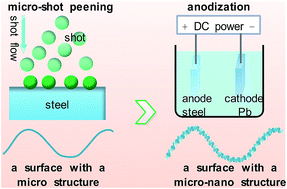
Micro-shot peening (MSP) was combined with subsequent anodization to produce a micro-nano structure on a carbon steel surface. It is to be noted that carbon steel is an engineering material rather than a non-engineering material. Non-engineering materials are commonly used substrates in studies relating to preparation of superhydrophobic surfaces. The results show that MSP produces a peened surface with a micro-scale structure. Subsequent anodization forms an anodized film with a nano-scale structure based on the peened surface. Hence, a steel surface with a micro-nano structure is produced by the combined method. Compared with the steel surface with a single micro-scale structure, the steel surface with a micro-nano structure exhibits a higher hydrophilicity. The steel surface with a micro-nano structure becomes superhydrophobic after modifying with fluoroalkylsilane.


1. Introduction

Micro-nano structures play a vital role in research areas such as superhydrophobic surfaces, self-cleaning coatings, anti-condensation coatings, anti-stick coatings and anti-fouling coatings.1–10 Barthlott and co-workers first reported the lotus effect and revealed the micro-nano hierarchical structure existing on plant leaves.11–15 Their findings have stimulated research interest in this area. In order to mimic the superhydrophobic plant leaf surface, researchers developed the nanocasting and ultraviolet nanoimprint lithography techniques.16–19 A real plant leaf serves as a template to prepare a superhydrophobic surface in these studies.

According to the Wenzel and Cassie–Baxter models,20,21 roughness is believed to affect wettability. Furthermore, superhydrophobic surfaces in nature are usually covered with micro-, nano- or micro-nano-scale asperities.22 Hence, roughness is very important for superhydrophobic surfaces. Surface energy is also important for superhydrophobic surfaces. There are two general ways to prepare a superhydrophobic surface:23 the first one is to create a rough surface and then modify it with a chemical agent to reduce surface energy; the second one is to directly fabricate asperities on a hydrophobic surface.

The preparation of a superhydrophobic surface involves many aspects. These include the following: the substrate; the method for fabricating a rough surface; the geometric pattern of the obtained rough surface; the chemical agent used for modifying the obtained rough surface. Many methods have been developed to fabricate and modify a rough surface; however, the chosen substrates are mostly non-engineering materials (e.g. silicon wafer, glass slide, polymer and textile fabric).24–28 In fact, engineering materials, especially metals like steel and aluminum alloy, might be required to have superhydrophobic surfaces. The first general way described above is suitable for fabricating a superhydrophobic surface on metal. Electro-deposition, chemical vapor deposition, physical vapor deposition and etching have been used to prepare rough surfaces on metals.29–35

In this work, we present a method in which micro-shot peening (MSP) is combined with subsequent anodization to fabricate a rough surface with multi-scale structure on carbon steel. This combined method is divided into two steps: MSP and anodization. MSP is proposed for producing a peened surface with a micro-structure. As a commonly used technique in the mechanical industry,36 shot peening will gain a new use. Anodization is proposed for fabricating a nano-structure on the peened surface. Anodization is usually used to coat Al, Mg or Ti with a dense or porous anodized film. The dense anodized film aims to strengthen the surface or protect the metal from corrosion.37 The porous anodized film is usually used in nano-technology,38 and also applied for superhydrophobic surfaces because of its nano-structure.39 However, anodizing Fe is not as easy as anodizing Al, Mg and Ti. Some researchers are engaged in the anodization of pure iron and stainless steel,40–42 but there are few reports on anodization of carbon steel.43 We implement anodization on shot-peened carbon steel to form an anodized film with a nano-scale structure. The anodized film is coupled onto the peened surface to form a surface with a micro-nano structure.

2. Experimental

2.1. Materials

The substrate is a carbon steel piece (20 mm × 20 mm × 5 mm). Micro-shots are stainless steel particles. Table 1 shows the chemical compositions of the carbon steel substrate and the stainless steel micro-shots. Silicon carbide abrasive papers with 120 to 1200 grit were used to grind steel pieces. A 1 μm diamond suspension was used to polish ground samples. Ammonium fluoride (NH4F, analytical reagent) and ethylene glycol (C2H6O2, analytical reagent) were purchased from Aladdin Industrial Corporation (Shanghai, China) for anodizing steel. Hexane (C6H14, analytical reagent) and 1H,1H,2H,2H-perfluorodecyltrichlorosilane (C10H4Cl3F17Si, analytical reagent) were from said company for modifying the surface of the steel.
Table 1 Chemical compositions of the carbon steel substrate and stainless steel micro-shots
Material Element, weight%
C Cr Ni Mn P S Si Fe
1045 carbon steel 0.42–0.50 0.6–0.9 0.04 max 0.05 max Balance
430 stainless steel 0.12 max 16–18 0.50 max 1 max 0.04 max 0.03 max 1 max Balance


2.2. Processing

2.2.1. Micro-shot peening. MSP is a shot-peening process in which the shots are micrometer in size. Steel pieces were ground using SiC abrasive paper, and then polished with a 1 μm diamond suspension. All polished samples were ultrasonically cleaned in acetone and thoroughly rinsed using DI water. MSP was carried out with an air-operated shot-peening device. The peening pressures were 0.1 MPa, 0.2 MPa and 0.3 MPa. The distance from the nozzle to the sample was 10 cm. The peening time was 2 min for each sample. All peened samples were washed using DI water and dried in air for the next process.
2.2.2. Anodization. Anodization was conducted in ethylene glycol electrolyte containing 0.1 M NH4F and 0.5 M H2O for 3 min, and the temperature of the electrolyte was 20 °C. A DC power supply was used to provide electricity and the anodization current density was 0.8 A dm−2.
2.2.3. Reducing surface energy. Chemical treatment was carried out in a C6H14 solution containing 0.1 vol% C10H4Cl3F17Si to reduce the surface energy. Samples were immersed in the solution at ambient temperature for 30 min.

2.3. Characterization

Chemical elemental analysis of the micro-shots was performed using an energy dispersive spectrometer (EDS) attached to a scanning electron microscope (SEM, S-3400, Hitachi, Japan). The shape and size of the micro-shots were analyzed using SEM. Macrograph analyses of the polished, unpolished and micro-shot peened sample (denoted as MSP-sample) were carried out using a stereo microscope (XTT, ZOUSUN, China). Surface roughness was measured using a profilometer (SJ-210, Mitutoyo, Japan). The profilometer can measure directly the surface profile of a sample, and then calculates the surface roughness from the surface profile. The average surface roughness was measured at five different positions on each sample. Surface topographies of MSP-samples and (MSP + A)-samples were characterized using SEM. The 3-D surface topography was investigated using an atomic force microscope (AFM, Solver p47-Pro, Russia) in semi-contact mode. Chemical composition of the anodized film was examined using EDS. The phase of the anodized film was identified using an X-ray diffractometer (XRD, D/MAX Ultima, Rigaku, Japan). Contact angles were measured with a contact-angle system (OCA, Data physics, Germany) using 5 μL water droplets at ambient temperature.

3. Results and discussion

Terms and abbreviations:

Micro-shot peening: a shot-peening process in which the shots are micrometer in size.

MSP: micro-shot peening.

A: anodization.

MSP + A: micro-shot peening plus anodization, the combined method.

MSP-sample: the sample subjected to MSP.

(MSP + A)-sample: the sample subjected to (MSP + A).

3.1. Peened surface with a micro-scale structure

Fig. 1a shows the result of the EDS analysis confirming the chemical composition of commercially available micro-shots. Fig. 1b shows the SEM image of micro-shots proving the sphere-shaped micro-shots with diameters of 30–80 μm.
image file: c6ra03734h-f1.tif
Fig. 1 (a) EDS spectrum of micro-shots; (b) SEM image of micro-shots.

Fig. 2 illustrates the preparation of the peened surface with a micro-scale structure. One micrometer-scale shot leaves one micrometer-scale indentation after it collides with the steel. A surface with a micro-scale texture could be created via multiple collisions.


image file: c6ra03734h-f2.tif
Fig. 2 Illustration of the preparation of a micro-scale structure on a steel surface.

There are a number of standard parameters of surface roughness. We choose Ra and Rz as parameters to describe the surface roughness. It should be noted that the roughness factor in Wenzel theory is different from surface roughness (i.e. Ra, Rz, etc.).44 We use Ra and Rz just to show the surfaces with a concave–convex texture. Fig. 3 shows surface roughnesses (Ra and Rz) for all samples. Each steel piece was cut from a steel bar. There are cutting marks on the surface of the steel piece (as shown in Fig. 4a). As a result, the measurement of the surface roughness of the unpolished sample is affected by the test orientation (moving direction of the profilometer probe). When the test orientation is parallel to cutting marks, Ra and Rz are 0.421 and 2.827 μm. When the test orientation is perpendicular to cutting marks, Ra and Rz are 2.352 and 14.620 μm. Such a rough surface will hinder the creation of a micro-scale structure on the steel surface. Hence, we have to grind and polish the original rough surface, and then perform MSP. The polished sample has a very small surface roughness. The MSP-samples have larger surface roughness than the polished samples. The surface roughness increases with increasing peening pressure. During the measurement of the surface roughness of MSP-samples, the test orientations are random. Measurement data of MSP-samples show that the surface roughness of the MSP-sample is independent of the test orientation. Compared with the surface of the polished sample, the surface of the MSP-sample is rough. Compared with the surface of the unpolished sample, the surface of the MSP-sample is smooth and homogeneous. Ra is the arithmetic average of the absolute values of the profile height deviations from the mean line. Thus, Ra can represent the ups and downs of a surface. Rz is the average distance between the highest peak and the lowest valley. Thus, Rz can represent the depth of indentations. For the MSP-sample, Ra and Rz are between those of the polished sample and the unpolished sample. Hence, the MSP-sample has a surface with a controlled roughness. In other words, MSP produces a surface with a controlled roughness.


image file: c6ra03734h-f3.tif
Fig. 3 Surface roughnesses (Ra and Rz) for all samples: (a) Ra; (b) Rz. Samples are numbered from (1) to (6): (1) the unpolished sample: the test orientation is parallel to cutting marks; (2) the unpolished sample: the test orientation is perpendicular to cutting marks; (3) the polished sample; (4) the MSP-sample, a peening pressure of 0.1 MPa; (5) the MSP-sample, a peening pressure of 0.2 MPa; (6) the MSP-sample, a peening pressure of 0.3 MPa.

image file: c6ra03734h-f4.tif
Fig. 4 Macrographs of: (a) the unpolished sample; (b) the polished sample; (c) the MSP-sample, a peening pressure of 0.1 MPa; (d) the MSP-sample, a peening pressure of 0.2 MPa; (e) the MSP-sample, a peening pressure of 0.3 MPa.

Fig. 4 shows macrographs of three kinds of surfaces. The surface of the unpolished sample is very rough and has cutting marks on it (Fig. 4a). The surface of the polished sample is smooth and there are a few scratches arising from grinding with sandpaper (Fig. 4b). Surfaces of MSP-samples have concave–convex textures (Fig. 4c–e). The SEM image of the concave–convex texture is shown in Fig. 5. Those ups and downs result from collisions during shot peening. The size of indentations can be identified as up to 30 μm. It demonstrates that MSP produces micro-scale indentations on the steel surface. Fig. 6 shows surface profiles. The polished sample has a smooth surface profile. The unpolished sample has a very rough surface profile. The MSP-sample has a controlled rough surface in comparison with the polished and unpolished samples.


image file: c6ra03734h-f5.tif
Fig. 5 SEM image of the concave–convex surface texture of the MSP-sample (peening pressure, 0.2 MPa).

image file: c6ra03734h-f6.tif
Fig. 6 Surface profiles of the unpolished sample, polished sample and MSP-sample (peening pressure, 0.2 MPa).

MSP produces a peened surface with a controlled roughness. This rough surface has a micro-scale concave–convex texture. It can be said that MSP produces a peened surface with a micro-scale structure.

3.2. Anodized film with a nano-scale structure

Fig. 7a shows the appearances of the MSP-sample and the (MSP + A)-sample. The MSP-sample has a peened surface with a concave–convex texture (Fig. 7a-1). The (MSP + A)-sample is coated with a colored anodized film (Fig. 7a-2). Fig. 7b shows surface roughnesses for two kinds of samples. The (MSP + A)-sample has a slightly lower roughness compared with the MSP-sample. This means that the surface roughness is slightly decreased after anodization. It is believed that dissolution of metal and formation of metal oxide film come about simultaneously during anodization.45 When the growth rate of oxide film is greater than the dissolution rate of metal, the oxide film grows constantly and the film thickness increases. We suggest that the slight decrease in surface roughness is due to the dissolution of metal. The MSP-sample and the (MSP + A)-sample have similar surface profiles (Fig. 7c).
image file: c6ra03734h-f7.tif
Fig. 7 (a-1) Macrograph of the MSP-sample; (a-2) macrograph of the (MSP + A)-sample; (b) surface roughnesses (Ra) of the MSP-sample and (MSP + A)-sample; (c) surface profiles of the MSP-sample and (MSP + A)-sample.

SEM images of surface topography are shown in Fig. 8. We made a comparison of surface topographies between the MSP-sample and the (MSP + A)-sample. At low magnification, a concave–convex surface topography can be seen for both the MSP-sample and the (MSP + A)-sample (Fig. 8a and c). At high magnification, no characteristic topography can be seen on the surface of the MSP-sample (Fig. 8b). However, a geometric pattern with nano-scale dimension can be seen on the surface of the (MSP + A)-sample (Fig. 8d and e). The (MSP + A)-sample underwent MSP and subsequent anodization, while the MSP-sample underwent only MSP. As discussed in Section 3.1, MSP produces a peened surface with a micro-scale concave–convex texture. Thus, a concave–convex surface topography can be found in both samples at low magnification. The geometric pattern found on the surface of the (MSP + A)-sample is attributed to anodization. In other words, anodization contributes an anodized film with a nano-scale pattern. This anodized film is formed on the concave–convex surface (i.e. the peened surface). The nano-scale pattern is coupled onto the micro-scale concave–convex texture. A micro-nano hierarchical structure is formed.


image file: c6ra03734h-f8.tif
Fig. 8 Surface topographies: (a) low-magnification SEM image of the MSP-sample; (b) high-magnification SEM image of the MSP-sample; (c) low-magnification SEM image of the (MSP + A)-sample; (d) and (e) high-magnification SEM images of the (MSP + A)-sample.

The 3-D surface topography (Fig. 9) captured using AFM in semi-contact mode further demonstrates that such a micro-nano hierarchical structure exists on the surface of the (MSP + A)-sample.


image file: c6ra03734h-f9.tif
Fig. 9 AFM image of the surface of the (MSP + A)-sample.

An EDS spectrum (Fig. 10a) for a region marked in a corresponding SEM image (Fig. 10b) indicates that the anodized film contains mainly Fe, O and C. Elemental maps (Fig. 10c) confirm a homogeneous distribution of oxygen. The presence of O and its homogeneous distribution demonstrate that an iron oxide film has been formed on the steel via anodization in the ethylene glycol electrolyte. Carbon is detected in the anodized film as the substrate is carbon steel.


image file: c6ra03734h-f10.tif
Fig. 10 (a) EDS spectrum of the anodized film formed on the (MSP + A)-sample. (b) Corresponding SEM image. For scanning a larger area, a low-magnification image was captured. (c) Elemental mapping of Fe, O and C.

Fig. 11 shows XRD patterns of the anodized film before and after thermal annealing. The thermal annealing was carried out in an argon atmosphere at 300 °C for 1 hour. Before the thermal annealing, only signals from steel substrate are present in the pattern (i.e. only three peaks of iron are observed, as shown in Fig. 11a). After the thermal annealing, oxide peaks appear in the pattern (Fig. 11b). This result suggests that the anodized film is amorphous or poorly crystalline. The thermal annealing induces an amorphous-to-crystalline transition. Thus, oxide peaks appear in the pattern after the thermal annealing.


image file: c6ra03734h-f11.tif
Fig. 11 XRD patterns of the anodized film (a) before and (b) after thermal annealing. Thermal annealing was carried out in an argon atmosphere at 300 °C for 1 hour.

3.3. Wettability

Fig. 12 shows results of contact angle measurements. Before reducing surface energy, all samples have a hydrophilic surface as their contact angles are less than 90°. The unpolished sample has a slightly smaller contact angle than the polished sample. The MSP-sample has a smaller contact angle than both the unpolished sample and the polished sample. The (MSP + A)-sample has the smallest contact angle compared with the other samples. It is believed that contact angle decreases with increasing roughness for a hydrophilic surface.46 The surface of the unpolished sample is more rough than that of the polished sample. Thus, the unpolished sample has a smaller contact angle than the polished sample. The MSP-sample has a surface roughness that is between that of the polished sample and the unpolished sample. However, the MSP-sample has a smaller contact angle than the unpolished sample. The reason for this is because the surface roughness of the unpolished sample is dependent on the direction of cutting marks. Unlike the unpolished sample, the MSP-sample has a surface with a micro-scale concave–convex texture and its surface roughness is independent of the test orientation. The surface of the (MSP + A)-sample is also hydrophilic and its contact angle is the smallest. As mentioned in Section 3.2., the surface of the (MSP + A)-sample exhibits a micro-nano structure. Such a surface consists of a lower peening layer and an upper anodized film. It has been reported that anodized films have high surface energy and show hydrophilicity.47–49 A surface with a hierarchical structure and a high surface energy shows higher hydrophilicity.50 Thus, the surface of the (MSP + A)-sample shows higher hydrophilicity.
image file: c6ra03734h-f12.tif
Fig. 12 Contact angles and optical images of water droplets before and after reducing the surface energy. I, the unpolished sample; II, the polished sample; III, the MSP-sample; IV, the (MSP + A)-sample.

After reducing the surface energy, contact angles for all samples are greater than 90°. The unpolished sample has a greater contact angle than the polished sample because of the larger surface roughness. With increasing roughness, contact angle increases for a hydrophobic surface.43 Due to the surface texture, the MSP-sample exhibits greater contact angle compared with the unpolished sample. The (MSP + A)-sample has a hierarchical surface topography. A surface with low energy means a reduced absorption. Hence, the contact angle of the (MSP + A)-sample after reducing the surface energy increases significantly, exhibiting superhydrophobicity.

4. Conclusions

In this study, a two-step method was successfully used to fabricate a surface with a micro-nano hierarchical structure on carbon steel. Micro-shot peening produces a peened surface with a micro-scale structure. An anodized film with a nano-scale structure is formed on the peened surface by subsequent anodization. The nano-scale structure is coupled onto the micro-scale structure. A micro-nano hierarchical structure is thus formed. The anodized film is an amorphous iron oxide layer. It starts to transform into crystals when a thermal annealing is applied. Before reducing the surface energy, all samples have a hydrophilic surface. The (MSP + A)-sample has the smallest contact angle in comparison with the other samples due to its hierarchical surface topography. After reducing the surface energy, contact angles for all samples are greater than 90°. The unpolished sample, the polished sample and the MSP-sample have a hydrophobic surface. The surface of the (MSP + A)-sample has a contact angle greater than 150° exhibiting superhydrophobicity. This is due to the hierarchical surface topography. In summary, the two-step combined method was used to fabricate a surface with a hierarchical structure. This surface is hydrophilic. After reducing the surface energy, this surface is superhydrophobic. The combined method together with chemical treatment fabricates a superhydrophobic surface on carbon steel.

Acknowledgements

This work was supported by Science and Technology Planning Project of Guangdong Province, China (grant no. 2013B010403027), China Postdoctoral Science Foundation (grant no. 2014M562149) and Natural Science Foundation of Guangdong Province, China (grant no. 2015A030310162).

References

  1. S. Anand, A. T. Paxson, R. Dhiman, J. D. Smith and K. K. Varanasi, ACS Nano, 2012, 6, 10122–10129 CrossRef CAS PubMed.
  2. L. Bocquet and E. Lauga, Nat. Mater., 2011, 10, 334–337 CrossRef CAS PubMed.
  3. X. Deng, L. Mammen, H. J. Butt and D. Vollmer, Science, 2012, 335, 67–70 CrossRef CAS PubMed.
  4. P. Kim, M. J. Kreder, J. Alvarenga and J. Aizenberg, Nano Lett., 2013, 13, 1793–1799 CrossRef CAS PubMed.
  5. Y. Lu, S. Sathasivam, J. Song, C. R. Crick, C. J. Carmalt and I. P. Parkin, Science, 2015, 347, 1132–1135 CrossRef CAS PubMed.
  6. J. Lv, Y. Song, L. Jiang and J. Wang, ACS Nano, 2014, 8, 3152–3169 CrossRef CAS PubMed.
  7. A. Tuteja, W. Choi, M. Ma, J. M. Mabry, S. A. Mazzella, G. C. Rutledge, G. H. McKinley and R. E. Cohen, Science, 2007, 318, 1618–1622 CrossRef CAS PubMed.
  8. N. Vogel, R. A. Belisle, B. Hatton, T. S. Wong and J. Aizenberg, Nat. Commun., 2013, 4 DOI:10.1038/ncomms3176.
  9. T. S. Wong, S. H. Kang, S. K. Tang, E. J. Smythe, B. D. Hatton, A. Grinthal and J. Aizenberg, Nature, 2011, 477, 443–447 CrossRef CAS PubMed.
  10. X. Zhang, L. Wang and E. Levänen, RSC Adv., 2013, 3, 12003–12020 RSC.
  11. W. Barthlott and C. Neinhuis, Planta, 1997, 202, 1–8 CrossRef CAS.
  12. W. Barthlott, C. Neinhuis, D. Cutler, F. Ditsch, I. Meusel, I. Theisen and H. Wilhelmi, Bot. J. Linn. Soc., 1998, 126, 237–260 CrossRef.
  13. R. Fürstner, W. Barthlott, C. Neinhuis and P. Walzel, Langmuir, 2005, 21, 956–961 CrossRef PubMed.
  14. K. Koch, B. Bhushan and W. Barthlott, Prog. Mater. Sci., 2009, 54, 137–178 CrossRef CAS.
  15. C. Neinhuis and W. Barthlott, Ann. Bot., 1997, 79, 667–677 CrossRef.
  16. K. C. Chang, H. I. Lu, C. W. Peng, M. C. Lai, S. C. Hsu, M. H. Hsu, Y. K. Tsai, C. H. Chang, W. I. Hung and Y. Wei, ACS Appl. Mater. Interfaces, 2013, 5, 1460–1467 CAS.
  17. M. Sun, C. Luo, L. Xu, H. Ji, Q. Ouyang, D. Yu and Y. Chen, Langmuir, 2005, 21, 8978–8981 CrossRef CAS PubMed.
  18. P. Ke, X. N. Jiao, X. H. Ge, W. M. Xiao and B. Yu, RSC Adv., 2014, 4, 39704 RSC.
  19. S. M. Lee and T. H. Kwon, Nanotechnology, 2006, 17, 3189 CrossRef CAS.
  20. A. Cassie and S. Baxter, Trans. Faraday Soc., 1944, 40, 546–551 RSC.
  21. R. N. Wenzel, Ind. Eng. Chem., 1936, 28, 988–994 CrossRef CAS.
  22. X. M. Li, D. Reinhoudt and M. Crego-Calama, Chem. Soc. Rev., 2007, 36, 1350–1368 RSC.
  23. C. H. Xue, S. T. Jia, J. Zhang and J. Z. Ma, Sci. Technol. Adv. Mater., 2010, 11, 033002 CrossRef.
  24. B. N. Sahoo and B. Kandasubramanian, RSC Adv., 2014, 4, 22053–22093 RSC.
  25. S. Nagappan and C. S. Ha, J. Mater. Chem. A, 2015, 3, 3224–3251 CAS.
  26. W. Qiu, D. Xu, B. Liu, L. Shen and Q. Guo, RSC Adv., 2015, 5, 71329–71335 RSC.
  27. Z. Chu and S. Seeger, Chem. Soc. Rev., 2014, 43, 2784–2798 RSC.
  28. B. Cortese, D. Caschera, F. Federici, G. M. Ingo and G. Gigli, J. Mater. Chem. A, 2014, 2, 6781–6789 CAS.
  29. J. L. Zhang, C. D. Gu, Y. Y. Tong, X. L. Wang and J. P. Tu, J. Electrochem. Soc., 2015, 162, D313–D319 CrossRef CAS.
  30. C. D. Gu and J. P. Tu, Langmuir, 2011, 27, 10132–10140 CrossRef CAS PubMed.
  31. Y. Liu, X. Yin, J. Zhang, S. Yu, Z. Han and L. Ren, Electrochim. Acta, 2014, 125, 395–403 CrossRef CAS.
  32. W. Wu, M. Chen, S. Liang, X. Wang, J. Chen and F. Zhou, J. Colloid Interface Sci., 2008, 326, 478–482 CrossRef CAS PubMed.
  33. L. Li, V. Breedveld and D. W. Hess, ACS Appl. Mater. Interfaces, 2012, 4, 4549–4556 CAS.
  34. F. De Nicola, P. Castrucci, M. Scarselli, F. Nanni, I. Cacciotti and M. De Crescenzi, Nanotechnology, 2015, 26, 145701 CrossRef PubMed.
  35. T. C. Rangel, A. F. Michels, F. Horowitz and D. E. Weibel, Langmuir, 2015, 31, 3465–3472 CrossRef CAS PubMed.
  36. M. Torres and H. Voorwald, Int. J. Fatigue, 2002, 24, 877–886 CrossRef CAS.
  37. Y. G. Ko, E. S. Lee and D. H. Shin, J. Alloys Compd., 2014, 586, S357–S361 CrossRef CAS.
  38. T. Kikuchi, T. Yamamoto, S. Natsui and R. O. Suzuki, Electrochim. Acta, 2014, 123, 14–22 CrossRef CAS.
  39. Y. Oikawa, T. Minami, H. Mayama, K. Tsujii, K. Fushimi, Y. Aoki, P. Skeldon, G. Thompson and H. Habazaki, Acta Mater., 2009, 57, 3941–3946 CrossRef CAS.
  40. H. E. Prakasam, O. K. Varghese, M. Paulose, G. K. Mor and C. A. Grimes, Nanotechnology, 2006, 17, 4285 CrossRef CAS.
  41. S. Minagar, C. C. Berndt, J. Wang, E. Ivanova and C. Wen, Acta Biomater., 2012, 8, 2875–2888 CrossRef CAS PubMed.
  42. W. Zhan, H. Ni, R. Chen, X. Song, K. Huo and J. Fu, J. Mater. Res., 2012, 27, 2417–2424 CrossRef CAS.
  43. T. Burleigh, T. Dotson, K. Dotson, S. Gabay, T. Sloan and S. Ferrell, J. Electrochem. Soc., 2007, 154, C579–C586 CrossRef CAS.
  44. R. N. Wenzel, J. Phys. Chem. A, 1949, 53, 1466–1467 CrossRef CAS.
  45. J. F. Vanhumbeeck and J. Proost, Corros. Rev., 2009, 27, 117–204 CAS.
  46. T. Chau, W. Bruckard, P. Koh and A. Nguyen, Adv. Colloid Interface Sci., 2009, 150, 106–115 CrossRef CAS PubMed.
  47. T. Sawase, R. Jimbo, A. Wennerberg, N. Suketa, Y. Tanaka and M. Atsuta, Clin. Oral Implants Res., 2007, 18, 680–685 CrossRef PubMed.
  48. X. Yang, B. Jiang, Y. Huang, Y. Tian, H. Chen, J. Chen and B. Yang, J. Biomed. Mater. Res., Part B, 2009, 90, 608–613 CrossRef PubMed.
  49. G. W. Critchlow, K. A. Yendall, D. Bahrani, A. Quinn and F. Andrews, Int. J. Adhes. Adhes., 2006, 26, 419–453 CrossRef CAS.
  50. F. Rupp, L. Scheideler, N. Olshanska, M. De Wild, M. Wieland and J. Geis Gerstorfer, J. Biomed. Mater. Res., Part A, 2006, 76, 323–334 CrossRef CAS PubMed.

Footnote

Electronic supplementary information (ESI) available. See DOI: 10.1039/c6ra03734h

This journal is © The Royal Society of Chemistry 2016
Click here to see how this site uses Cookies. View our privacy policy here.