DOI:
10.1039/C6RA03479A
(Paper)
RSC Adv., 2016,
6, 40895-40899
Influences of nitrogen partial pressure on the optical properties of copper nitride films
Received
6th February 2016
, Accepted 10th April 2016
First published on 12th April 2016
Abstract
Copper nitride (Cu3N) films are made under different nitrogen pressures via radio frequency reactions and magnetron sputtering techniques. Scanning electron microscopy, X-ray diffraction, UV-visible spectrophotometry, and fluorescence spectrophotometry are conducted to test and analyze the structures and optical properties of the films. The films produced under distinct nitrogen pressures possess compact surfaces and even similar particle sizes. In addition, the Cu3N (111) crystal faces are mainly formed at low nitrogen pressures, whereas the Cu3N (100) crystal faces are mainly generated at high nitrogen pressures. The photo-induced luminous band of the Cu3N films is concentrated in the blue-violet area. Moreover, the optical band gap (Eg) of the films varies within the range of 1.23–1.91 eV and increases along with R. This variation is caused by the change of vacancy centers inside the film crystal and the concentration of elementary copper atoms that causes a distinct defect energy level.
Copper, which is a cheap and environmentally friendly element, is an abundant natural resource. Cuprous compounds are also ideal luminous materials. In recent years, photo-induced laminating research has achieved a series of successes.1,2 Cu3N crystal, which has become a research focus for semiconductor materials, has also gained considerable attention from various researchers for its distinct structure and performance.3–7 This crystal can replace disposable optical storage Te-based inorganic phase change materials because of its simplicity and lack of toxicity.8–10 Given its low decomposition temperature, Cu3N can be used as a buffer layer for integrated circuit, a barrier layer of low magnetic resistance for a tunnel junction, and a template for self-assembled materials.11 It can also be used as a new battery material and catalyst additive material because of its unique chemical activity.12–14 In addition, Cu3N is a competitor15,16 for field emission materials and has wide application prospects for its good electron emission properties.
Cu3N possesses an anti-methyltrioxorhenium crystal structure. In the Cu3N crystal, the s energy band of the Cu atom can overlap with the p energy band of the N atom, thereby forming a filled band. Thus, this crystal is an insulator. The Cu atom does not occupy a compact position in the crystal lattice (111) of the Cu3N crystal. However, it leaves many interspaces in the crystal structure and therefore makes it easy for other atoms to fill in the center vacancy of the Cu3N crystal. Cu3N vacancy doping causes a change in the crystal structure and leads Cu3N to transform into a semiconductor or even a conductor.17–19
Numerous research reports on the optical properties of Cu3N films are available. The optical band gap (Eg) of Cu3N films is calculated theoretically as ∼0.9 eV,20–22 but experimental results show that the value is within the range of 1.1–1.9 eV and changes according to different production conditions.23,24 The variation in the Eg of the Cu3N films is attributed to the preparation conditions.25–27 Sahoo reported that the Eg of the Cu3N films increases with increasing deposition pressure, and the indirect and direct band gaps are in the range of 1.17–1.68 and 1.72–2.38 eV, respectively.28 Pierson achieved the same results, but the Eg ranges from 0.25 eV to 0.83 eV.29 The stoichiometry of the Cu3N films is determined by the substrate temperature, thereby affecting the optical band gap of the films.30 Doping can also change the optical properties of the Cu3N films. These films show evident metal characteristics after Ti doping, and the optical band gap of the films increases with increasing Ti doping.18 The electroluminescence of the Cu3N nanocrystal has also been investigated. Cu3N nanocrystals can be used as a nanoscale light source.31 However, no literature reports exist on the electroluminescence performance of Cu3N films.
With its distinct structure, the chemical properties of Cu3N are exceptional, but the relationship among the causes of performance change, change of crystal structure, and production process is still unknown. Thus, further study is necessary. In this study, magnetron sputtering techniques are used to produce Cu3N films. The crystal structure of the Cu3N films, optical properties, and the micro-mechanism of Eg change under different nitrogen partial pressures are also investigated.
1 Experimental section
1.1 Sample preparation
We designed the RF reaction magnetron sputtering equipment system. The system was manufactured by the Shenyang Institute of Metal Research, Chinese Academy of Sciences. Copper (99.99%) was used as a target and a nitrogen (99.999%) and argon (99.999%) mixture was employed as the working gas. (100) P silicon slice and quartz plates were used as substrates. The substrates were soaked in acetone and alcoholic solution, individually, cleaned using ultrasonic waves for 20 min, washed with deionized water, and dried in a drying oven before placing them into the vacuum room. In every deposition, the background pressure in the vacuum room was lower than 1.0 × 10⁻³ Pa. Pre-sputtering in an Ar (20 SCCM) environment was conducted for 10 min before every sputtering. The surface and base of the target were cleaned and nitrogen was pumped into the deposited Cu3N film samples. In sputtering, the total flow of nitrogen and argon was fixed at 40 SCCM; the sputtering pressure and frequency power (Pf) were 1.0 Pa and 300 W, respectively. In the experiment, R(N2/[N2 + Ar]) was used as the research parameter, where R can be 0.1, 0.2, 0.4, and 0.8. In deposition, the substrate temperature was fixed at 150 °C and the duration time (T) was 15 or 20 min.
1.2 Sample characterization
The surface of Cu3N films and the structure of the film crystals were characterized using a JSF-2100 field emission scanning electron microscope and a D/max 250 full-automatic X-ray diffractometer, respectively. The photoluminescence spectrum of the films with an indoor temperature was acquired with a Cary eclipse fluorescence spectrophotometer and the exciting light was a He–Cd laser with a wavelength of 190 nm. A TU-1800 UV-visible (UV-vis) spectrophotometer was used to obtain the transmission spectrum of the films.
2 Results and analysis
2.1 Film surface
The colors of the films made are closely related to the content amounts of both Cu3N and Cu. The target used was pure copper and the Cu3N content increased with increasing R. Therefore, the film samples changed their color from yellow of Cu to brownish black of Cu3N.
Fig. 1a shows the Cu3N films deposited on the surface of monocrystalline silicon, which is compact and tight; the deposition power and nitrogen partial pressure (R) were 300 W and 0.4, respectively. Fig. 1b shows the corresponding sectional view; the inner structure of the film samples is also compact and the film thickness is around 500 nm. Combining the deposition time and thickness of other samples, the average growth speed of Cu3N films is about 33 nm min−1 and decreases with increasing R. Fig. 2 shows the EDS spectrum of the Cu3N films. The figure also illustrates detailed data of the apparent concentration of various elements and atomic mass percentages.
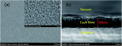 |
| | Fig. 1 Scanning electron microscopy spectrum of Cu3N films (preparation conditions: Pf = 200 W, R = 0.4, T = 15 min): (a) surface image and (b) sectional view. | |
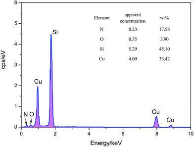 |
| | Fig. 2 EDS spectrum of Cu3N films (R = 0.2). | |
As observed from the EDS spectrum of Cu3N films, the atomic mass percentage of Cu3N films produced has distinct R (Table 1). Table 1 shows that the percentage of nitrogen atom mass first increases clearly with increasing R, whereas the percentage of copper atom mass decreases. Second, Cu3N films contain highly concentrated O. Analysis shows that O mainly originated from two aspects: first, the oxygen content left at the bottom of vacuum room; and second, the water and oxygen contained in air, which is absorbed on the film surface before testing. In addition, the large Si content in the films is caused by the monocrystalline silicone piece as a deposition substrate.
Table 1 EDS spectrum data of element (E) wt% of the Cu3N thin films deposited at different R
| E |
R = 0.1 |
R = 0.2 |
R = 0.4 |
R = 0.8 |
| N |
14.94 |
16.30 |
17.58 |
27.91 |
| O |
1.65 |
2.96 |
3.90 |
1.91 |
| Si |
41.20 |
39.95 |
45.10 |
37.74 |
| Cu |
42.21 |
40.79 |
33.42 |
32.44 |
2.2 Analysis of the film microstructure
Fig. 3 shows the X-ray diffraction (XRD) spectra of film samples with different R values (deposition power is 300 W). With an increase of R, the diffraction peaks of Cu3N films (100) and (110) at around 23° and 33°, respectively, become increasingly stronger and the change of the (100) crystal face along with the partial pressure is more evident than that of the (110) crystal face. However, the diffraction peak of the Cu3N films (111) around 41° gradually becomes weaker, which means that the films have preferential growth orientations with different R values. The Cu3N film grows on (111) crystal face with low R, whereas those on (100) and (110) crystal face with high R. Thus, R can affect the law of preferred Cu3N film crystal growth orientation.32 The reason may be as follows: with low R, the absorbing nitrogen atom is inserted into the crystal lattice of copper atoms, thereby forming a Cu–N chemical bond and films. The films also exhibit the same growth law as that of Cu (111) and grow into the Cu3N (111) face. With high R, sufficient N atoms are present and these atoms can be combined with Cu on the target or substrate surface to form Cu–N. Subsequently, the films develop the Cu3N (100) and (110) surfaces based on the principle that the lowest crystal free energy has preferential growth.
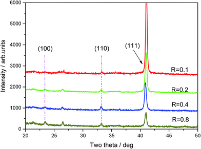 |
| | Fig. 3 X-ray diffraction spectra of Cu3N films deposited at different R. | |
Furthermore, with Bragg's law (1) and the cubic system interplanar distance law (2), the lattice constant of the Cu3N films can be acquired.
| |
λ = 2dhkl![[thin space (1/6-em)]](https://www.rsc.org/images/entities/char_2009.gif) sinθ sinθ
| (1) |
| |
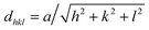 | (2) |
where
λ refers to the X-ray wavelength;
θ refers to the diffraction angle;
h,
k, and
l refer to the crystal face constants; and
dhkl refers to the interplanar distance of the (
hkl) crystal plane family. The lattice constant of the Cu
3N films produced in distinct conditions can also be acquired (
Table 2).
Table 2 Lattice constants (a) of Cu3N films deposited at different R and the lattice constant reported by others references
The average lattice constant of the Cu3N films acquired from the experiment is around 3.851 Å; the minimum and maximum values are 3.831 and 3.872 Å, respectively. The lattice constant increases along with the decrease of R. This value is intermediate between those reported by other researchers (Table 2), which may be caused by the distinct production processes of the films.
2.3 Optical transmission properties of the films
Fig. 4a shows the UV-vis transmission spectrum of Cu3N films produced with different R values. The Cu3N films have strong absorption properties in blue and purple light regions. The films also exhibit good transmission rates in the infrared region, which satisfies the character that the photoluminescence spectrum has an excellent luminous zone in the blue and purple light regions. According to the film transmission spectrum curve and based on the film optical constant law (3) that is calculated from the transmission spectroscopy, the absorption coefficients of the films in the weak, medium, and strong absorption regions can be calculated as follows:where d refers to the film thickness and T refers to light transmittance. Using the Tauc eqn (4), the Eg of the films can be calculated as follows:24| | |
(αhν)1/2 = A(hν − Eg)
| (4) |
where α, hν, and A refer to the absorption coefficient, photon energy, and a constant, respectively. Using this equation, the Eg range of the Cu3N films made with specific values of R is within 1.23–1.91 eV, as shown in Fig. 4b. The Eg of the Cu3N films rapidly increases with the increase in R and then the growth rapidly decreases. With the continuous increase of R, Eg also has a large increase. When R is 0.8 (lattice constant is 3.872 nm), the Eg of the films increases rapidly to 1.91 eV. This value is close to the reported literature value.29 When the film lattice constant is larger than 3.868 nm, it is a conductor; however, when it is smaller than 3.868 nm, it is an insulator.
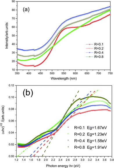 |
| | Fig. 4 UV-visible spectra of Cu3N films deposited by different R (a) and its Eg (b). | |
2.4 Luminescence characteristics of light emitted from the films
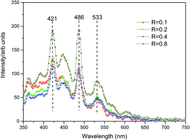
Fig. 5 shows the photoluminescence spectrum of Cu3N films produced with different R values and indoor temperatures; their photoluminescence spectrum is mainly concentrated in the blue and purple light areas. For each film sample, three peaks of PL are observed at 421, 486, and 533 nm. According to the changes of R, the intensity of the distinct photoluminescence peak also varies. However, the homogeneous phases at peaks of 421 and 486 nm are relatively large. The comparison results of purple and blue light emissions of Cu3N are attributed to the following: (1) defect energy level of vacancies in the center of the films and electron transition between compound defects; (2) electron transition of Cu, as an interstitial atom, from defect energy level to valence band; and (3) electron transition between interface defect and valence band around the Cu3N grain boundary. The Eg of the films is co-affected by these factors. Furthermore, the intrinsic light band gap of the Cu3N films is within the range of 2.33–2.95 eV, which is easily obtained through the peak of PL. This value is obviously higher than the Eg range of 1.23–1.91 eV acquired from the Tauc equation. This finding means that the interface defects near the Cu3N crystal boundary is far away from the bottom of conduction band.
 |
| | Fig. 5 Photoluminescence spectra of Cu3N films deposited by different R. | |
3 Analysis and discussion
In our opinion, the aforementioned changes of the Eg of Cu3N films are mainly attributed to low R; the excessively sputtered elementary copper atoms react with nitrogen at the surface and bottom of the target and subsequently deposit on the substrate. The formation of Cu3N films is mainly through absorbing nitrogen atoms that insert into the copper lattice, thereby forming a Cu–N bond. Simultaneously, some copper atoms deposited on the film surface have not formed a bond with nitrogen. Therefore, the central vacancy of the Cu3N lattice still contains many copper atoms and the Cu atom filling provides weak localized electrons. For electrons combined on the Cu3N lattice with a covalent bond, these weak localized electrons are non-localized and their existence can change the electron density distribution inside the films. Thus, the films did the characteristics of a semiconductor or even a conductor that has a low Eg. When the R is large, the highly concentrated nitrogen atmosphere provides sufficient N atoms to react with Cu atoms and form Cu–N bonds. Consequently, no Cu atoms fill in the gaps and the Eg of the films is large. Therefore, the films are almost insulators.
4 Conclusion
The Cu3N films are made with distinct R and RF frequencies via RF reaction and magnetron sputtering techniques. The appearances of the Cu3N films, lattice structures, and optical characteristics are characterized using scanning electron microscopy, XRD analysis, and UV-vis spectroscopy. The film surface is compact and the particle sizes are average. With the increase of R, the growth rate of the Cu3N (111) lattice is slightly decreased, whereas the Cu3N (100) and (110) lattices grow at a relatively higher speed. The Eg of the film samples is within the range of 1.23–1.91 eV. With the increase of R, the Eg first increases rapidly and then the growth speed decreases. Finally, the growth rate increases with increasing R. This change is mainly caused by the central vacancy of films and non-bonded Cu atoms causing change of defects, which further affects the electron density change inside the film lattice. We conclude that the Cu3N films prepared by this method have varying optical band gaps and possess excellent photoluminescence properties. The films can be employed as an optical protective layer and nanometer-size light sources.
Conflict of interests
The authors declare no conflicts of interests with regard to the publication of this study.
Acknowledgements
The authors are grateful to the National Natural Science Foundation of China (No. 11364011), Guangxi Natural Science Foundation (No. 2015GXNSFAA139004), and Innovation Project of Guangxi Graduate Education (No. YCSZ2015164) for their financial support.
References
- P. C. Ford, E. Cariati and J. Bourassa, Chem. Rev., 1999, 99, 3625–3647 CrossRef CAS PubMed.
- Q. S. Zhang, T. Komino, S. P. Huang, S. Matsunami, K. Goushi and C. Adachi, Adv. Funct. Mater., 2012, 22, 2327–2336 CrossRef CAS.
- X. A. Li, Q. F. Bai, J. P. Yang, Y. T. Li, L. X. Wang, H. Y. Wang, S. L. Ren, S. L. Liu and W. Huang, Vacuum, 2013, 89, 78–81 CrossRef CAS.
- P. X. Xi, Z. H. Xu, D. Q. Gao, F. J. Chen, D. S. Xue, C. L. Tao and Z. N. Chen, RSC Adv., 2014, 4, 14206–14209 RSC.
- X. D. Xu, N. Y. Yuan, J. H. Qiu and J. N. Ding, Mater. Res. Bull., 2015, 65, 68–72 CrossRef CAS.
- J. Park, K. Jin, B. Han, M. J. Kim, J. Jung, J. J. Kim and W. Lee, Thin Solid Films, 2014, 556, 434–439 CrossRef CAS.
- X. Y. Fan, Z. J. Li, A. Meng, C. Li, Z. G. Wu and P. X. Yan, J. Mater. Sci. Technol., 2015, 31, 822–827 Search PubMed.
- T. Maruyama and T. Morishita, Appl. Phys. Lett., 1996, 69, 890–891 CrossRef CAS.
- Z. G. Ji, Y. H. Zhang and Y. Yuan, Mater. Lett., 2006, 60, 3758–3760 CrossRef CAS.
- Y. H. Zhao, J. Y. Zhao, T. Yang, J. Zhang, J. P. Yang and X. A. Li, Ceram. Int., 2016, 42, 4486–4490 CrossRef CAS.
- T. Wang, X. J. Pan, X. M. Wang, H. G. Duan, R. S. Li, H. Li and E. Q. Xie, Appl. Surf. Sci., 2008, 254, 6817–6819 CrossRef CAS.
- A. S. Powell, Z. Stoeva, R. I. Smith, D. H. Greogry and J. J. Titman, Phys. Chem. Chem. Phys., 2011, 13, 10641–10647 RSC.
- B. S. Lee, M. Yi, S. Y. Chu and J. Y. Lee, Chem. Commun., 2010, 46, 3935–3937 RSC.
- R. Deshmukh, G. B. Zeng, E. Tervoort, M. Staniuk, D. Wood and M. Niederberger, Chem. Mater., 2015, 27, 8282–8288 CrossRef CAS.
- A. L. Ji, C. R. Li, Y. Du, L. B. Ma, R. Song, R. Huang and Z. X. Cao, Nanotechnology, 2005, 16, 2092–2095 CrossRef CAS PubMed.
- T. Wang, R. S. Li, X. J. Pan, P. Z. Zhang, M. Zhou, X. Song and E. Q. Xie, Chin. Phys. Lett., 2009, 26, 066801–066803 CrossRef.
- J. G. Zhao, S. J. You, L. X. Yang and C. Q. Jin, Solid State Commun., 2010, 150, 1521–1524 CrossRef CAS.
- X. Y. Fan, Z. G. Wu, G. A. Zhang, C. Li, B. S. Geng, H. J. Li and P. X. Yan, J. Alloys Compd., 2007, 440, 254–258 CrossRef CAS.
- G. Sahoo and M. K. Jain, AIP Adv., 2015, 5, 107223 CrossRef.
- Y. Wen, J. G. Zhao and C. Q. Jin, Phys. Rev. B: Condens. Matter Mater. Phys., 2005, 72, 214116–214124 CrossRef.
- M. G. Moreno-Armenta and A. Martínez-Ruiz, Solid State Sci., 2004, 6, 9–14 CrossRef CAS.
- U. Hahn and W. Weber, Phys. Rev. B: Condens. Matter Mater. Phys., 1996, 53, 12684–12693 CrossRef CAS.
- D. M. Borsa and D. O. Boerm, Surf. Sci., 2004, 548, 95–105 CrossRef CAS.
- F. Fendrych, L. Soukup, L. Jastrabik, M. Sicha, Z. Hubicka, D. Chvotova, A. Tarasenko, V. Studnicka and T. Wagner, Diamond Relat. Mater., 1999, 8, 1715–1719 CrossRef CAS.
- J. R. Xiao, Y. W. Li and A. H. Jiang, J. Mater. Sci. Technol., 2011, 27, 403–407 CAS.
- Z. G. Wu, W. W. Zhang, L. F. Bai, J. Wang and P. X. Yan, Acta Phys. Sin., 2005, 54, 1687–1692 CAS.
- G. M. Moreno-Armenta, G. Soto and N. Takeuchi, J. Alloys Compd., 2011, 17, 1471–1476 CrossRef.
- G. Sahoo, S. R. Meher and M. K. Jain, Mater. Sci. Eng., B, 2015, 191, 7–14 CrossRef CAS.
- J. F. Pierson, Vacuum, 2002, 66, 59 CrossRef CAS.
- S. Ghosh, F. Singh, D. Choudhary, D. K. Avasthi, V. Ganesan, P. Shah and A. Gupta, Surf. Coat. Technol., 2001, 142–144, 1034–1039 CrossRef CAS.
- A. Strozecka, J. C. Li, R. Schuermann, G. Schulze, M. Corso, F. Schulz, C. Lotze, S. Sadewasser, K. J. Franke and J. I. Pascual, Phys. Rev. B: Condens. Matter Mater. Phys., 2014, 90, 195420–195427 CrossRef.
- L. X. Yang, J. G. Zhao, Y. Yu, F. Y. Li, R. C. Yu and C. Q. Jin, Chin. Phys. Lett., 2006, 23, 426–427 CrossRef CAS.
- A. Miura, T. Takei and N. Kumada, J. Aust. Ceram. Soc., 2014, 2, 326–328 CrossRef.
- G. Paniconia, Z. Stoevaa, H. Dobersteinb, R. I. Smithc, B. L. Gallagherd and D. H. Gregory, Solid State Sci., 2007, 9, 907–913 CrossRef.
- T. Maruyama and T. Morishita, J. Appl. Phys., 1995, 78, 4104–4107 CrossRef CAS.
|
| This journal is © The Royal Society of Chemistry 2016 |
Click here to see how this site uses Cookies. View our privacy policy here. 
 ,
Aihua Jiang*,
Yaping Zeng and
Jiafeng Ma
,
Aihua Jiang*,
Yaping Zeng and
Jiafeng Ma


