
 Open Access Article
 This Open Access Article is licensed under a
 Creative Commons Attribution 3.0 Unported Licence
Effect of the aromatic precursor flow rate on the morphology and properties of carbon nanostructures in plasma enhanced chemical vapor deposition
K.
Lehmann
ab,
O.
Yurchenko
*ab and
G.
Urban
ab
aFreiburg Materials Research Centre (FMF), University of Freiburg, Freiburg, Germany
bDepartment of Microsystems Engineering (IMTEK), Laboratory for Sensors, University of Freiburg, Freiburg, Germany. E-mail: olena.yurchenko@fmf.uni-freiburg.de; Tel: +49 7612034781
First published on 4th April 2016
Abstract
Understanding the effects of the synthesis parameters on the morphology and electrochemical properties of nanocarbon layers is a key step in the development of application-tailored nanostructures. In this paper we used an aromatic carbon as a new kind of precursor for the synthesis of carbon based nanostructures by plasma enhanced chemical vapor deposition (PECVD). Complex precursor molecules enable a new degree of influence over the atomic structure of PECVD synthesized carbons. Here, we report on the synthesis and characterization of the nanostructures resulting from varied flow rates of p-xylene used as carbon precursor. By changing the flow rate of the precursor, three different morphologies with graphitic character were synthesized. The resulting structures were carbon nanofibers (CNF), freestanding carbon nanowalls (fCNW) and interconnected carbon nanowalls (iCNW), formed at flow rates of 3 ml h−1, between 1 and 3 ml h−1 and less than 1 ml h−1, respectively. Structural characterization by transmission electron microscopy and Raman spectroscopy indicate a lower defect density for the CNF in comparison to the CNW nanostructures. The electrochemical characterization of the oxygen reduction reaction onset potential and effective surface area feature a significantly higher onset at around −171 mV and an electrochemically active surface area of 0.76 μm−1 for the iCNW compared to −196 mV, 0.61 μm−1 and 0.22 μm−1 for the fCNW and CNF, respectively. The similarities in defect density and differences in activity observed for the iCNW and fCNF suggest that the kind of the defects determines the electrochemical properties. Thus, the iCNW was identified as the most appropriate morphology for further investigations.
1. Introduction
Carbon materials have long been established as electrode materials in diverse electrochemical applications, such as batteries, fuel cells, supercapacitors, for several reasons.1–3 Graphite, the most famous carbon material with sp2 hybridization, is low-priced and offers good electrical conductivity and high chemical stability which make it a great electrode material. Regrettable, it lacks porosity limiting its potential to reach high energy densities.4 Activated carbon is a form of amorphous carbon. It is low-priced as well and possesses a huge surface area making it a perfect material for supercapacitors.5,6 However, the enhancement of surface area in activated carbon is accompanied with increasing of porosity which leads to poorer electrical conductivity of the layers restricting its widespread utilization in diverse electrochemical devices or presuppose the adding of conductive additives.7–9 Graphene, an aromatic monolayer of carbon atoms, features in return both high electrical conductivity and high surface area making it to a material with promising electrochemical properties. However, graphene has a high tendency to restack and agglomerate due to strong π–π interactions between the sheets. This causes a distinct decrease of active surface area as well as porosity and electrochemical performance.10The plasma enhanced chemical vapor deposition (PECVD) method represents a promising approach for stepwise growth of vertically aligned carbon nanostructures of different shapes. Different plasma sources have been used to synthesize vertical nanostructures in literature. Most commonly, direct current (DC), microwave (MW) and radio frequency (RF) induced plasma were used. In DC PECVD, the plasma is generated between two electrodes when a sufficient potential is applied. The substrate is usually placed on the cathode. Limitations arise when the substrate is not electronically conductive. In contrast, MW and RF plasma work without electrodes. Between them, MW plasma has the advantage of working at higher pressures, up to several thousand pascal, and has a high deposition rate. On the other side, RF PECVD is a low temperature deposition method and of advantage when coating temperature sensitive substrates.11–13
The vertical alignment of the nanostructures in all three cases results from the electric field of the plasma.14,15 The application of plasma in PECVD method, compared with CVD, greatly decreases process temperature and allows to improve alignment and direction of the nanomaterial growth.16 The spectrum of nanostructures fabricated by PECVD includes diamond-like carbon, carbon nanotubes, carbon nanofibers, carbon nanowalls and other structures.17–19 Simple aliphatic compounds like CH4, C2H2, CF4, C2F6 are usually used as the carbon source.20–22 The PECVD growth process enables the realization of well-defined porous electrode architectures with tunable and controllable morphology, in which the irreversible aggregation of nanostructures, typical for solution-based synthesis procedures, apart from template assisted methods, is prevented.10 The structural diversity of nanoscaled structures available by PECVD should result in the variation of physical as well as chemical properties typical for non-aligned carbon structures.1,23–25 This is especially promising for applications that need a high surface to volume ratio, while maintaining a high signal and power transfer efficiency. Examples are electrochemical energy conversion devices, like fuel cells, batteries or capacitors, and sensors.26–28
Therefore, understanding the effect of synthesis parameters on the nanoscale/mesoscale structure, as well as the electrochemical properties of nanostructured carbons, are indispensable preconditions to achieve electrode performance maximization, thus contributing to successful implementation in energy devices and sensors.
In this paper we report on the synthesis and characterization of three diverse carbon nanostructures (CN). The CN were grown using inductively coupled plasma enhanced chemical vapor deposition (IC-PECVD) without a catalyst and with aromatic p-xylene as a carbon precursor. By considering the plasma chemistry of p-xylene, the growth mechanism and the effect of the flow rate on the nanostructure morphology were discussed. Facile adjustment of the precursor flow rate resulted in alternating nanostructures. Carbon nanofibers (CNF), freestanding carbon nanowalls (fCNW) and interconnected carbon nanowalls (iCNW) were synthesized, iCNW showed the highest oxygen reduction reaction onset and effective surface area. The influence of monomer flow rate on the structure, morphology and electrochemical properties was studied by means of Raman spectroscopy, scanning and transmission electron microscopes as well as cyclic voltammetry, respectively, in order to understand the correlation between nano-/mesostructure and electrochemical properties.
2. Material and methods
Synthesis
Carbon nanostructures (CN) were synthesized in PECVD process using an inductively coupled plasma (ICP)-source according to reference (Hussein and Shoukat et al.)29,30 and applying p-xylene as carbon precursor. The IC-PECVD process is based on report from Xu et al.18 A schematic of a modified version is visible in Fig. 1.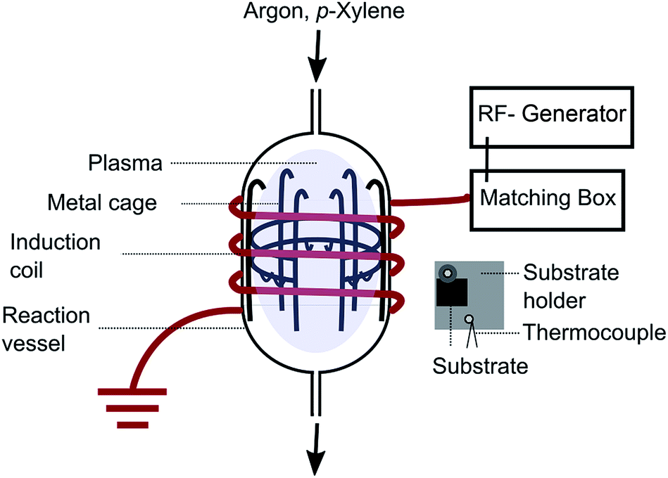 | ||
| Fig. 1 Schematic of the IC-PECVD plant. | ||
The reactor used for the synthesis is made of a quartz reaction vessel with 85 mm in height and with an internal diameter of 70 mm. An open steel cage, to hold the substrate holder, is situated inside the reaction vessel. The substrate, fixed on a substrate holder, is mounted parallel to the gas flow direction. The plasma is driven by a 13.56 MHz RF generator (PFG 300 from Hüttinger Elektronik) adjusted to a power supply of 150 W for 20 minutes for all depositions. 150 W was used to ensure a controllable growth speed, because growth speed was observed to increase exponentially with increased power input, while 20 min growth time produced a well recognizable film and guaranteed high reproducibility. The substrate temperature at these settings was 450 °C. The energy is transferred to a cylindrical coil made of 4 mm copper wire wrapped around the quartz vessel in six turns and grounded on the end. The functionality is explained in ref. 25.
The vacuum in the reactor was created by a rotary pump (Alcatel T2060C). The pressure monitoring was done by means of two compact pirani gauges (Pfeiffer PCR260). Process pressure was varied between 4.6 and 7.5 Pa, depending on the precursor supply rate. Argon gas (99.999%) was introduced at 10 sccm by an electronic mass flow controller (Brooks 5850E). The carbon precursor was an aromatic hydrocarbon p-xylene (Sigma-Aldrich, puriss. p.a., ≥99.0%) which was deaerated for 30 minutes by bubbling with argon. Precursor supply was ensured and adjusted by a syringe pump (Harvard PHD 2000) and a needle valve (Pfeiffer EVR 116). The substrate was chosen to be precleaned silicon wafer pieces coated with titanium nitride. They were mounted on metal plates, which were fixed to a cylindrical metal grid in the reactor. The metal plate surface temperature was determined by a k-type thermocouple.
The structural and electrochemical characterization of carbon nanostructures
Scanning electron microscopy (SEM) (Quanta 250 FEG), transmission electron microscopy (TEM) (Zeiss LEO 912), Raman spectroscopy (Olympus BX40) and X-ray Photoelectron Spectroscopy (XPS) (Physical Electronics 5600 ci) were used to study morphology, nanoscale structure and composition of the samples. The Raman spectroscopy plots were evaluated by a Lorentzian fit of the D-, G- and D′-peak.The electrochemical properties were investigated with the help of cyclic voltammetry (CV) (Autolab PGSTAT30) in a three electrode setup. The reference electrode was an Ag/AgCl electrode in 3 M KCl solution, a platinum counter electrode and the sample with a diameter of 2.5 mm as working electrode were used. For each sample and investigation, three measurements on different places of the sample were performed.
For the investigation of the ability to catalyze oxygen reduction reaction (ORR), the CV measurements were performed in 0.1 M KOH solution saturated with nitrogen or air at a scan rate of 10 mV s−1. The effective surface area (Aeff) was determined by CV measurements in solution of 50 mM KCl and 5 mM potassium ferricyanide K3[Fe(CN)6] at six scan rates (ν) ranging from 5 to 200 mV s−1. In this context, the examination of Aeff has proved to be useful to gain in-depth understanding of specific characteristics of graphene-based materials.31 The anodic peak current obtained from the CVs was plotted over ν1/2. Finally, Aeff was determined with the help of the resulting slope and the Randles–Sevcik eqn (1.1).
| Ipa = (2.69 × 10⁵)n3/2Aeff(Dν)1/2C0 | (1.1) |
3. Results and discussion
Nanostructures growth & structural characterization
The variation of the liquid precursor flow rate in the range of 0.5 to 5 ml h−1 leads to the formation of three different morphologies, carbon nanofibers (CNF), freestanding carbon nanowalls (fCNW) and interconnected carbon nanowalls (iCNW). The growth process does not need a catalyst which was confirmed by parallel synthesis on glassy carbon, glass and titanium nitride coated silicon wafer. For the examination of the flow rate effect on the morphology and the structure height, three samples in each flow range were synthesized. The deposition time and power was 20 min and 150 W for all samples, respectively.SEM images of the corresponding morphologies are shown in Fig. 2. To produce CNF, depicted in Fig. 2a, a flow rate between 3 and 5 ml h−1 was necessary, the resulting height of the fibers varies between 2.2 and 6 μm. Fig. 2b shows fCNW growing at a flow rate of 1–2 ml h−1 to a height of 1.4 to 2.2 μm. Below 1 ml h−1 the resulting morphology was iCNW structure, shown in Fig. 2c. iCNW reach a height between 1.1 and 1.6 μm. The height differences are probably caused by accuracy constraints of the feed supply rate. It should be noted that the distinction between fCNW and iCNW is fluent. The transition from fCNW to iCNW happens when the vertical sheets connect with each other resulting in a consistent mesh like structure. This means, that from 2 ml h−1 downwards no fundamental structure change happens, except a decreasing of the wall size and simultaneous increasing of the wall number at lower feed flow rates.
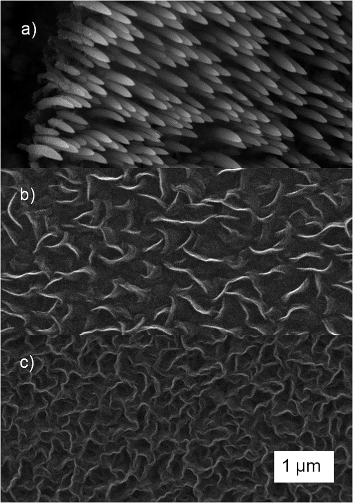 | ||
| Fig. 2 SEM pictures of tilted view of CNF (a) and top view of fCNW (b) and iCNW (c). | ||
In Fig. 3 the resulting height of the structure is plotted over the flow rate of the precursor. Below 3 ml h−1, the dominating CNF nanostructure changes to CNW. While the flow rate changes from 0.5 to 3 ml h−1, only an increase in height of around 0.5 μm or 33% can be observed. According to Ostrikov et al. 2013,13 the kind of nanostructure forming depends on supply and consumption of the precursor, whereby the consumption of the precursor depends on the surface temperature, which in turn is influenced by the power supply. Because the power supply is constant for every synthesis performed, no changes should occur for a power limited process. The growth of CNW, which happens at flow rates below 3 ml h−1, does not alter a lot with the changing flow rate indicating power supply limitation. Above 3 ml h−1, fiber growth occurs and the height triples with the flow rate increasing from 3 to 5 ml h−1. It follows that the fiber growth is limited by the precursor supply.
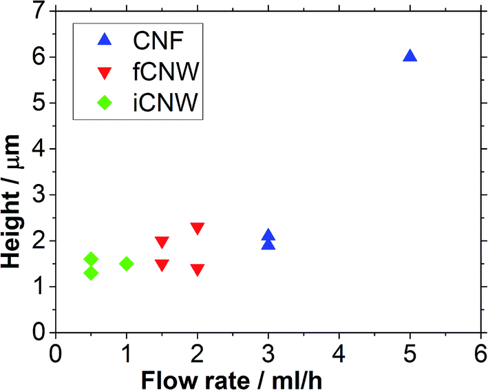 | ||
| Fig. 3 Height of each sample plotted over the flow rate during synthesis. | ||
The nanostructure of the obtained carbon structures was examined by Raman spectroscopy through investigation of the D- and G-peaks (Fig. 4).
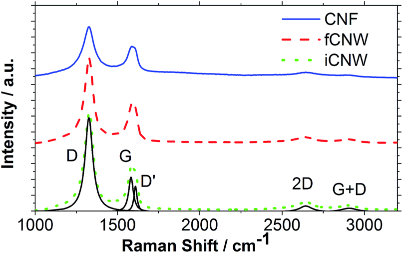 | ||
| Fig. 4 Raman spectrum of a CNF, fCNW and iCNW sample with all visible peaks marked and shown by a Lorentzian fit of the iCNW sample. | ||
The D-peak, D′-peak and the G + D-peak, located at 1325 cm−1, 1609 cm−1 and 2907 cm−1, respectively, are caused by the disorder in the material structure.33 The G-peak located at 1588 cm−1 features the graphitic character of the material, which is responsible for the ability of the material to conduct electricity. The D′-peak, which overlaps with the G-peak, has to be subtracted from the G-peak. The size, shape and position of the 2D peak depend on the layers thickness of the material. However, above 5 layers the peak becomes undistinguishable from bulk graphite.34 CNW are reported to be 2–3 layers thick at the tip but the base, which dominates the Raman response, consists of more than 5 layer.19,35 The SEM and TEM examinations in Fig. 2 and 6 confirm this, as the visible dimensions are several tens of nm wide at least. For this reason, no further examinations of the 2D were performed. Defects, indicated by the D-peak, represent edges as well as vacancies in the graphitic carbon layer and are responsible for adsorption as well as electron transfer processes.36 Therefore, defects are very important for electrochemical activity of the material. The results exhibit that all three morphologies are based on sp2 bonded graphitic carbon. By calculating the ID/IG ratio the relative amount of disorder in sp2 carbons can be deduced.34 The calculation results show that iCNW and fCNW with ID/IG ratio of 2.6 possess a similar amount of defects, while CNF, the samples with the highest growth rate, tend to have a ID/IG ratio of less than 1.5 exhibiting a smaller amount of defects. The small width of the D-peaks of 60 to 90 cm−1 (Table 1) is typical for non-amorphous carbons.37–39
| ν D, cm−1 | W D, cm−1 | ν G, cm−1 | W G, cm−1 | ν D′, cm−1 | W D, cm−1 | I D/IG | |
|---|---|---|---|---|---|---|---|
| CNF | 1324 | 90.67 | 1589 | 72.52 | 1.49 | ||
| fCNW | 1326 | 63.37 | 1583 | 51.27 | 1610 | 23.07 | 2.57 |
| iCNW | 1325 | 64.06 | 1582 | 50.38 | 1609 | 23.14 | 2.58 |
To make sure that the carbon nanostructures do not contain a second element, the iCNW samples were investigated by XPS. The XPS plot in Fig. 5 shows a strong C1s peak at 284.6 ± 0.2 eV and a weak O1s peak at 532.6 eV. The dominance of the C1s peak confirms that the nanostructures consist mainly of carbon. The position of C1s peak is typical for sp2 hybridized carbon. The weak O1s peak could come from the physical adsorption of oxygen or water from air.40–42
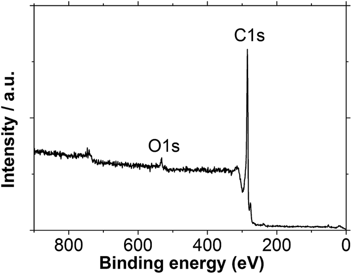 | ||
| Fig. 5 XPS spectrum of iCNW structure as example. | ||
A closer look at the sample structure with TEM (Fig. 6) confirms the Raman results, that CNW structures have a higher defect density than CNF structure. The CNF structure (Fig. 6a–c) shows no edges and a smooth surface, while fCNW and iCNW (Fig. 6d and e, respectively) are vertically grown walls of graphene, which results in a high amount of thin graphene layers with edges. Additionally, the sheets of iCNW structure are twisted and bend in different directions indicating an increased number of atomic defects in the graphene layer.43
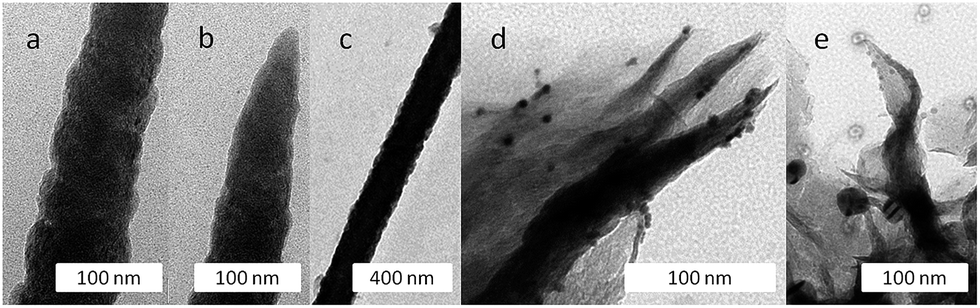 | ||
| Fig. 6 TEM images of CNF (a–c), fCNW (d) and iCNW (e). | ||
The dark, spherical particles observed in Fig. 6d and e are impurities from previous characterizations, they are not found in uncharacterized samples. The light, spherical particles observed in Fig. 6e are carbon nuclei which we believe to grow on the walls resulting in an irregular surface.
In general, CNF structures encompass a wide range of nanostructures which have a fiber like morphology in common. They are classified in three types, parallel, fishbone or bamboo like nanostructure. The parallel type, usually called multi walled carbon nanotubes (MWCNT), lacks graphitic edge sites on its lateral surface. Bamboo type has exposed graphitic edge sites at the transition between the links resulting in a bamboo like fiber, while fishbone type CNF's lateral surface consists of edge sites entirely offering a huge active surface for adsorption and electron transfer. It was, however, in literature reported, that fishbone type CNF need a catalyst at the fiber tip to grow, which is not present in this research.44–47 Close examination of TEM images (Fig. 6a and b) indicates that fibers are likely building from stacked spherical structures implicating a bamboo type nanostructure.
In Fig. 7, schematics of a parallel type CNF (a), a bamboo type CNF with accessible edge sites between the links (b) and the cross-section of a CNW (c) are shown. These schematics were adapted from ref. 48. The small graphene sheets attached to a CNF recognized in Fig. 5c indicates that the sphere growth resulting in CNF and the sheet growth resulting in CNW happen simultaneously at different growth rates and under different constraints.
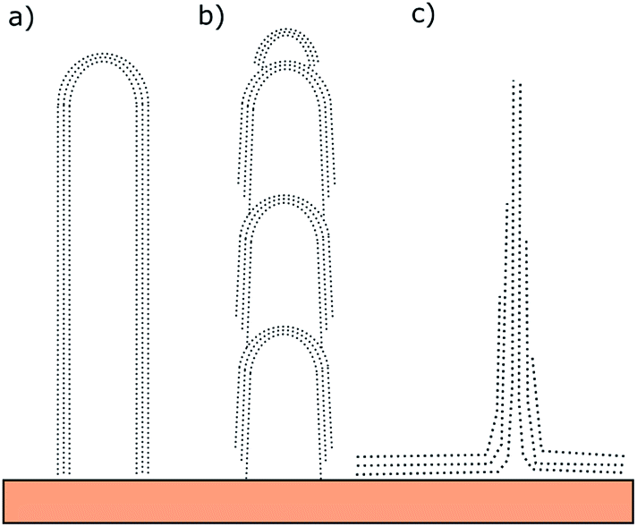 | ||
| Fig. 7 Cross view schematic of parallel type CNF (a), bamboo type CNF (b) and CNW (c). | ||
Plasma chemistry: comparison with conventionally used precursors
In following, we consider chemical reactions which are expected to take place in presence of p-xylene precursor and lead to the varying nanostructure formations. Especially, the formation of CNFs growing at applied conditions without catalyst is of interest, since the growth of carbon nanotube and nanofiber, irrespective of type, by both CVD and PECVD methods, usually require catalyst.49–51The two consecutive steps are necessary for growth of aligned nanostructures in PECVD, the formation of nucleation sites and vertical growth under the influence of an electric field. Thereby, the carbon source, beside the substrate, is supposed to play a dominating role in nanocarbon synthesis. This results from the strong influence of the generation process of building units by bond stability in the respective precursor and its carbon content.52–54 By PECVD of conventionally employed hydrocarbons, e.g. C2H2 or CH4, and fluorocarbons, e.g. CF4, CHF3, or C2F6, mainly the different types of reactive carbon dimers (C2) are believed to be the initial building units in carbon nanostructure growth.53,55 C2 is generated by dehydration or bond dissociation of precursors through interactions with Ar, Ar ions, metastables or by electron collision and possible radical recombination. Starting from C2, the higher mass carbon clusters CnHx+ are formed which initiate the formation of critical nuclei and the growth process.52,53,55,56
The employing of p-xylene as aromatic unit bearing precursor should results in the modification of the nucleation and growth process. The C–H bond at a methyl group (CH3) with the bond dissociation energy lower than 89 kcal mol−1† is the weakest bond in p-xylene.57 The C–H bond in benzene ring has dissociation energy of about 113 kcal mol−1, while the average dissociation energy of a bond between carbon atoms in the benzene ring is estimated to be in the range of 132–138 kcal mol−1.57,58 Thus, the stability of aromatic ring is considerably higher than that of the methyl group. We suggest that the process starts with the production of the reactive p-xylyl radicals (Scheme 1), since the initial formation of these radicals was observed by pyrolysis of p-xylene.59,60 Moreover, the p-xylyl radicals are able to undergo the condensation reaction through elimination of H2 molecules under formation of polycyclic aromatic (2,6-dimethylanthracene), which can further participate in nucleation and growth process.60 This reaction path should require plasma of comparatively low energy. For comparison, the dissociation energy of C–H bond in acetylene (HC![[triple bond, length as m-dash]](https://www.rsc.org/images/entities/char_e002.gif) C–H) is about 133 kcal mol−1 and that of the first C–H bond in methane (H3C–H) of 105 kcal mol−1, which is significantly higher than that of H2C–H in p-xylene.57
C–H) is about 133 kcal mol−1 and that of the first C–H bond in methane (H3C–H) of 105 kcal mol−1, which is significantly higher than that of H2C–H in p-xylene.57
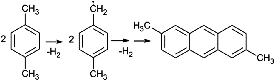 | ||
| Scheme 1 The first possible reaction path in p-xylene PECVD process: formation of reactive p-xylyl radicals and their condensation to polycyclic aromatic 2,6-dimethylanthracene. | ||
According to calculations and mass spectra analysis performed by Koseki et al.,61 the generation of C8H10+ and low-mass ions (Scheme 2), for example by electron collision, is also expected as the second reaction path. This path requires however plasma of higher energy, because of the quite high ionization potential of p-xylene (about 9 eV).
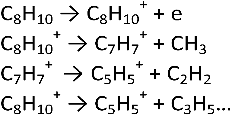 | ||
| Scheme 2 The second possible reaction path in p-xylene PECVD process: p-xylene ionization and formation of low-mass ions and species.61 | ||
The probability of the condensation reaction (Scheme 1) should increase with the rise of p-xylyl radical's concentration. In contrast, the probability of C8H10+ formation and its decomposition to low-mass ions should not change or decrease with a rising precursor flow rate. Thus, we expect that, at higher precursor flow rates, the first reaction path is more favorable than the second one. We believe that the different kinetics of these possible reaction sequences is the reason for the control of nanostructure formation by precursor flow rate.
Also Ostrikov et al. emphasized,13 that the kind of nanostructure forming depends on supply (formation of reactive building units) and consumption of the precursor (growth process), whereby the consumption of the precursor depends on the surface temperature, which in turn is influenced by the power supply. Because the power supply is constant for every synthesis performed, no changes should occur for a power limited process. The growth of CNW, which happens at flow rates below 3 ml h−1, does not alter a lot with the changing flow rate indicating power supply limitation. Above 3 ml h−1, fiber growth occurs and the height triples with the flow rate increasing from 3 to 5 ml h−1. It follows that the fiber growth is limited by the precursor supply.
We assume that the formation of CNF, which possess lower number of defects, is rather resulted from the first reaction path, while CNW nanostructures with higher defect density and high amount of carbon nuclei are generated mainly from low-mass ions follow second reaction path. The low-mass non aromatic ions should create additional lattice defects.
Electrochemical characterization
To determine the influence of the morphology of nanocarbon films on electrochemical characteristics, the activity towards oxygen reduction reaction (ORR), the effective surface area and the capability to heterogeneous electron transfer were investigated. For that purpose, the onset potential Eonset of ORR62 as well as the extent and reversibility of the redox reaction of ferricyanide were examined. Additionally, from the cyclic voltammogram (CV) of ORR, the capacitive part of the current in CV was derived, and used as an indication for different degrees of sample wetting.Fig. 8a shows CVs performed in air (blue) and nitrogen (black) saturated solution for the Eonset determination of ORR. The ORR Eonset of this sample is determined as the crossing of the two tangents at −202 mV. A tilting of the curves can be observed to different extent in all measurements. This might result from solution seeped through the CNW outside the measurement area, creating regions with a very high ions transfer resistance. The second reason is possible conductivity limitations of the substrate. The capacitive part of the CV current (CPC) was derived from the difference between the forward and the backward sweep of the CV at −100 mV, as is highlighted in Fig. 8a.
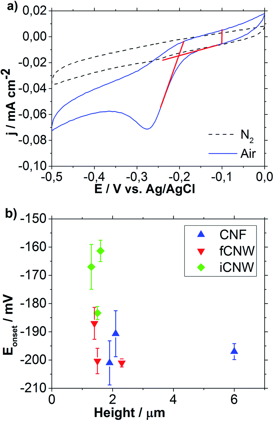 | ||
| Fig. 8 Cyclic voltammogram recorded in nitrogen and air saturated 0.1 M KOH solution (a); summary of ORR Eonset plotted over the sample height (b). | ||
The results of Eonset determination plotted over the sample height are shown in Fig. 8b. No correlation between the height of the respective nanostructure and the ORR Eonset can be observed, although a clear shift towards positive Eonset in case of iCNW is visible. Both fCNW and iCNW should have an abundance of edge plane sites resulting from the vertical growing graphene sheets, which have a strong ability for the adsorption of O2 and are widely understood to have a higher catalytic and electrochemical activity as graphitic basal planes.63,64 The iCNW structures additionally have bend and twisted sheets, which indicate atomic structure defects in the sheets.43 The higher density of atomic structure defects might cause a change in the Fermi level and thereby a lowering of the work function of iCNW.65,66 The work function lowering is associated with an increase in activity towards ORR.67,68 The CNF and fCNW structures feature a similar ORR Eonset found on average slightly above −200 mV which is apparently more positive than the onset of glassy carbon electrode observed at −220 mV. Because of the fact that the electrochemical properties of glassy carbon are similar to those of basal plane graphite, the higher reactivity of CNF and fCNW towards ORR should originate from a large number of edge planes obtained in these materials.63 While the edge plane seems obvious for fCNW, their existence in case of CNF strongly suggests the bamboo type structure for CNF, considering the findings of TEM analysis.
The CPC was used as an indicator for the degree of sample wetting. In Fig. 9a the influence of the structure height on the CPC is shown. Fig. 9b is used to examine the relationship between the Eonset and the surface area of nanostructure being in contact with the electrolyte.
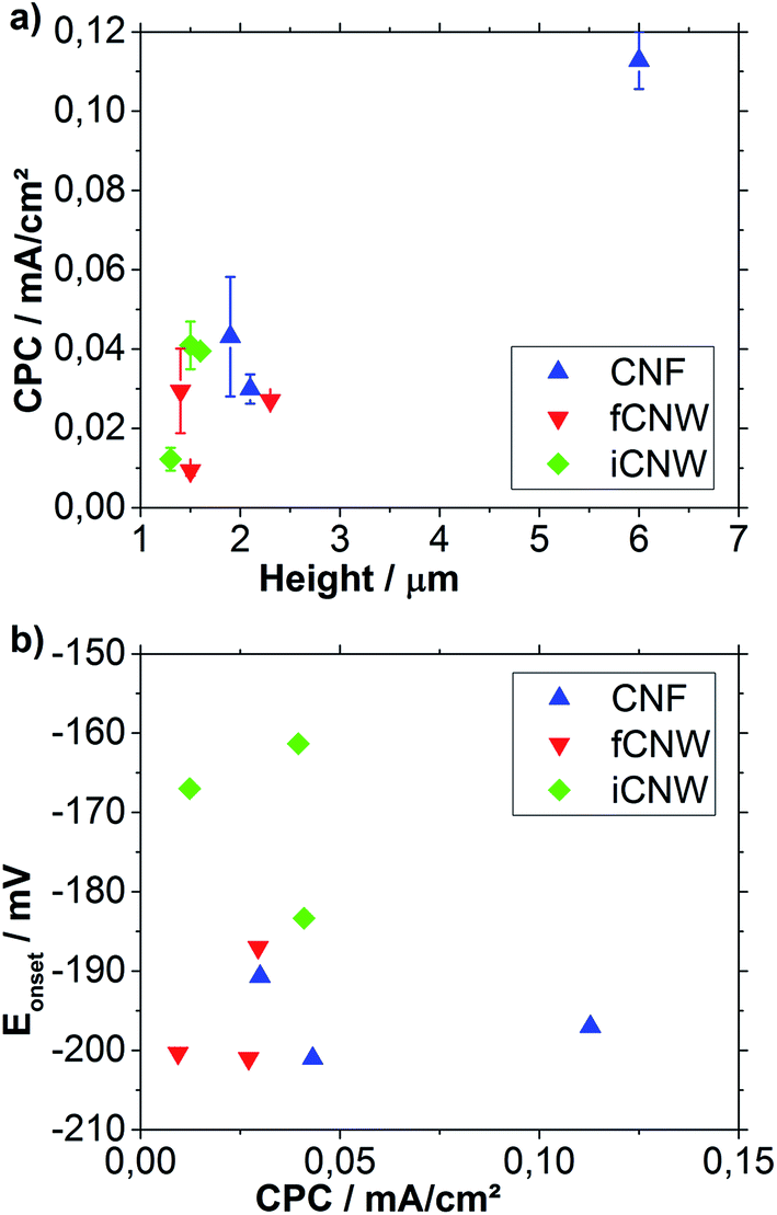 | ||
| Fig. 9 CPC plotted over the sample height (a), Eonset plotted over the CPC (b). | ||
Besides observation of high value distribution in Fig. 9a, an increase of the CPC with the height of the nanostructures can be noticed for large height differences. Apart from that, iCNW structures seem to have a slightly larger CPC than fCNW probably resulted from smaller pores and thereby higher surface area. CNF have a larger capacitive current CPC indicating a larger surface area resulting from the different morphology and bigger height of nanostructures. A big problem emerging with mesoporosity of carbon structures is the increasing of hydrophobicity, which leads to incomplete wetting of the structure and thereby to deviation in CPC measured.69 For assessment of relationships between catalytic activity towards ORR and the wetting of carbon surfaces expressed by CPC, the ORR Eonset was plotted over the CPC (Fig. 9b). While there is no correlation between ORR Eonset and capacitive current CPC observable for CNF and fCNW, iCNW seems to have a better Eonset with the higher CPC. Because the height of those iCNW samples is very similar, a higher CPC can implicate a higher degree of wetting. The structure of iCNW, shown in Fig. 6e, features a high number of graphene edges inside the material. These edges are assumed to be the active spots for ORR.70 A higher degree of wetting should result in more active spots in solution, which also generates a higher CPC and an increased positive shift of Eonset, in case of a process with kinetic limitations. For fCNW the influence of the wetting is negligible, the exposed graphene edges are mostly located at the top of the material. The result is that the active spots of fCNW are in the solution even at a low degree of wetting. No relationship between CPC and Eonset can be observed for CNF as well as fCNW indicating that, unlike for iCNW, the amount of active spots is not the limiting factor. Different reaction limiting factors for iCNW compared to fCNW and CNF suggest a fundamental difference in the kind of active spots available.
To evaluate the performance of the three morphologies as an electrode material, the corresponding nanostructures were applied as electrode in CV measurements of redox reaction of potassium ferricyanide K3[Fe(CN)6]. Thereby the separation between the peak potentials ΔEp in CV and the active surface area (Aeff) of electrode were determined. Determining Aeff provides a direct parameter for the amount of electrochemical active spots on a sample. Whilst the peak potential difference between the anodic and the cathodic peak ΔEp give information about reaction reversibility which is 59 mV for a perfectly reversible one electron reaction71 as well as electron transfer activity. The edge plane pyrolytic graphene with a high number of edge plane sites, which are responsible for fast heterogeneous charge transfer, usually exhibit a small value of ΔEp.46 All investigated nanostructures exhibited values below 70 mV for scan rates under 10 mV s−1 evidencing that all materials feature sufficient amount of defects for fast transfer kinetic. The results also show an increase of ΔEp with increasing scan rate to around 150 mV for 200 mV s−1. The increase of ΔEp has been explained as a result of contamination by oxygen and water adsorption at the active spots, which affects the electrode kinetics.72,73
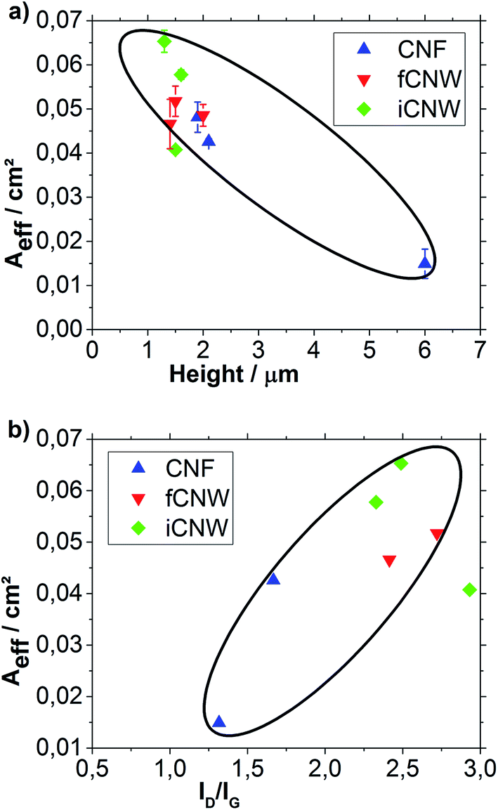
The results of the Aeff measurements are shown in Fig. 10a. The assessment focus is set on the samples inside the marked area, because the one iCNW sample standing out differs significantly in ORR Eonset, CPC, Aeff and ID/IG from other samples, which indicate its deterioration caused by some unknown process, like synthesis contamination or pore blockage.
 | ||
| Fig. 10 A eff plotted over the sample height (a) and the ID/IG ratio (b). | ||
In contrast to the CPC, Aeff decreases with rising sample height. This trend denotes the reduction of active spots in samples with larger growth rate. Consequently, a higher growth rate produces a large surface, which yields the high CPC, but fewer active spots, which is reflected in a small Aeff. For CNF growth this means that the amount of links forming the fiber decreases, while the links get larger making the CNF more similar to parallel type rather than bamboo type. Considering the growth mechanism, this evolution could be explained by a decreasing nucleation rate on the fiber tips resulting in continued link growth. Decreasing nucleation rate might arise from lower plasma temperature caused by the higher particle density. Analysis of the samples with similar height reveals that CNW have on average a higher Aeff than CNF. Moreover, iCNW appear to have a larger Aeff than fCNW originating from a higher number in graphitic edges.
When examining an influence of ID/IG ratio on Aeff (Fig. 10b) clear relationships between a higher ID/IG ratio and a higher Aeff can be seen confirming the key role of defects as active spots in electron transfer.
The last step is examination of the relationship between the ORR Eonset and Aeff (Fig. 11). For better comparability, the investigated samples in marked area exclude the likely corrupted iCNW sample and the especially large CNF sample. The different morphologies inside the marked area show a clear correlation between a higher catalytic activity towards oxygen reduction and an increased Aeff for iCNW which are the most reactive nanostructures followed by fCNW and then CNF. The resemblance between fCNW and CNF in Aeff and Eonset values suggests that not the wall growth mechanism is responsible for the increased reactivity towards ORR and higher number of active spots for electron transfer. The strong differentiation of iCNW from fCNW in ORR Eonset and Aeff supports this view. The higher reactivity of iCNW, especially with respect to ORR, despite of the similar ID/IG values supposes that not only the amount of defects is an important parameter for electrochemical reactions, but that the kind of defects is at least as important for the electrochemical activity of nanocarbon materials. In case of iCNW, the increased amount of atomic defects in the graphitic layer, apparent in their twisted structure, can also cause an increased reactivity caused by a lowering of the work function.
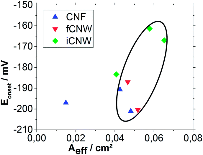 | ||
| Fig. 11 E onset plotted over the calculated Aeff. | ||
4. Conclusions
Three different types of nanostructured carbon films, CNF, fCNW and iCNW, were synthesized by PECVD method through variation of monomer flow rate and comprehensively studied by structural and electrochemical characterization. The results of SEM and TEM analysis indicate two different growth mechanisms for CNF and CNW nanostructures (fCNW and iCNW) also producing different amounts of defects which were identified by examination of ID/IG value from Raman spectra. It was observed that the decreasing of monomer flow rates lead to the increasing amount of defects identified by SEM and TEM as graphitic edge sites. However, the differences in electrochemical activity between CNF and fCNW were small, with the ORR Eonset at −196 mV and Aeff between 0.46 μm−1 (CNF) and 0.61 μm−1 (fCNW). Moreover, a generally higher electrochemical activity was observed for iCNW, Eonset = −171 mV and Aeff = 0.76 μm−1, despite the comparable values of ID/IG with fCNW. In contrast to fCNW, iCNW nanostructures exhibit twisted walls which can originate from atomic defects in graphene sheets. These findings led us to conclude that the kind of defects is a determining factor for electrochemical activity. Finally, iCNW with interconnected walls were determined as the nanostructures with the best electrochemical activity. The formation of defects and realizing of different structures were discussed with respect to plasma chemistry of p-xylene precursor.The results of this work demonstrate the potential control over the structure and properties of carbon CN, by adjustment of the precursor flow rate.
Acknowledgements
We gratefully acknowledge the German Research Association (DFG) for supporting this work within the Research Training Group (GRK 1322) “Micro Energy Harvesting”, Dr R. Thomann for TEM measurements and Dr L. Ledernez as well as Dr F. Olcaytug for technical support.References
- E. Antolini, Appl. Catal., B, 2009, 88(1–2), 1 CAS.
- X. Ji, K. T. Lee and L. F. Nazar, Nat. Mater., 2009, 8(6), 500 CrossRef CAS PubMed.
- Supercapacitors for peak-power demand in fuel-cell-driven cars, ed. R. Kötz, S. Müller, M. Bärtschi, B. Schnyder, P. Dietrich, F. N. Büchi, A. Tsukada, G. G. Scherer, P. Rodatz and O. Garcia, 2001 Search PubMed.
- J. P. Howe, J. Am. Ceram. Soc., 1952, 35(11), 275 CrossRef CAS.
- E. Frackowiak, Phys. Chem. Chem. Phys., 2007, 9(15), 1774 RSC.
- A. G. Pandolfo and A. F. Hollenkamp, J. Power Sources, 2006, 157(1), 11 CrossRef CAS.
- E. Frackowiak and F. Béguin, Carbon, 2001, 39(6), 937 CrossRef CAS.
- J. Gamby, P. L. Taberna, P. Simon, J. F. Fauvarque and M. Chesneau, J. Power Sources, 2001, 101(1), 109 CrossRef CAS.
- G. Wang, Z. Shao and Z. Yu, Nanotechnology, 2007, 18(20), 205705 CrossRef.
- M.-Q. Zhao, Q. Zhang, J.-Q. Huang, G.-L. Tian, J.-Q. Nie, H.-J. Peng and F. Wei, Nat. Commun., 2014, 5, 1 CrossRef.
- A. Bisht, S. Chockalingam, O. S. Panwar, A. K. Srivastava and A. K. Kesarwani, Fullerenes, Nanotubes, Carbon Nanostruct., 2014, 23(5), 455 CrossRef.
- Z. Bo, Y. Yang, J. Chen, K. Yu, J. Yan and K. Cen, Nanoscale, 2013, 5(12), 5180 RSC.
- K. Ostrikov, E. C. Neyts and M. Meyyappan, Adv. Phys., 2013, 62(2), 113 CrossRef CAS.
- K. Ostrikov and A. B Murphy, J. Phys. D: Appl. Phys., 2007, 40(8), 2223 CrossRef CAS.
- I. Levchenko, K. Ostrikov, A. E. Rider, E. Tam, S. V. Vladimirov and S. Xu, Phys. Plasmas, 2007, 14(6), 63502 CrossRef.
- C. Daraio and S. Jin, in Nanotechnology for Biology and Medicine, ed. G. A. Silva and V. Parpura, Springer, New York, 2012, p. 27 Search PubMed.
- Y. H. Wu, T. Yu and Z. X. Shen, J. Appl. Phys., 2010, 108(7), 71301 CrossRef.
- B. Xu, T. Li, X. Liu, X. Lin and J. Li, Thin Solid Films, 2007, 515(17), 6726 CrossRef CAS.
- K. Davami, M. Shaygan, N. Kheirabi, J. Zhao, D. A. Kovalenko, M. H. Rümmeli, J. Opitz, G. Cuniberti, J.-S. Lee and M. Meyyappan, Carbon, 2014, 72, 372 CrossRef CAS.
- J. Chen, Z. Bo and G. Lu, Vertically-oriented graphene: PECVD synthesis and applications, 2015 Search PubMed.
- H. J. Cho, H. Kondo, K. Ishikawa, M. Sekine, M. Hiramatsu and M. Hori, Carbon, 2014, 68, 380 CrossRef CAS.
- S. Kondo, S. Kawai, W. Takeuchi, K. Yamakawa, S. Den, H. Kano, M. Hiramatsu and M. Hori, J. Appl. Phys., 2009, 106(9), 94302 CrossRef.
- J.-P. Tessonnier, D. Rosenthal, T. W. Hansen, C. Hess, M. E. Schuster, R. Blume, F. Girgsdies, N. Pfänder, O. Timpe and D. S. Su, Carbon, 2009, 47(7), 1779 CrossRef CAS.
- A. A. Balandin, Nat. Mater., 2011, 10(8), 569 CrossRef CAS PubMed.
- A. Mostofizadeh, Y. Li, B. Song and Y. Huang, J. Nanomater., 2011, 2011(3), 1 CrossRef.
- B. Y. Park, R. Zaouk, C. Wang and M. J. Madou, J. Electrochem. Soc., 2007, 154(2), P1 CrossRef CAS.
- B. Fang, J. H. Kim, M. Kim and J.-S. Yu, Chem. Mater., 2009, 21(5), 789 CrossRef CAS.
- M. Al-Halhouli, J. Kieninger, O. Yurchenko and G. Urban, Appl. Catal., A, 2016, 517, 12 CrossRef CAS.
- L. Hussein, Decorated carbon nanostructured electrodes for biofuel cell and biosensor application, Schluchsee, Vierjahreszeiten, 2011 Search PubMed.
- R. Shoukat, S. Jindal, D. Xavier, L. Hussein, L. Ledernez, Y. Thomann, R. Thomann, F. Olcaytug and G. Urban, Influence aromatic hydrocarbon source on the morphology of carbon nanostructures grown with IC-PECVD, in preparation.
- D. Qazzazie, M. Beckert, R. Mülhaupt, O. Yurchenko and G. Urban, Electrochim. Acta, 2015, 186, 579 CrossRef CAS.
- M. P. Siswana, K. I. Ozoemena and T. Nyokong, Electrochim. Acta, 2006, 52(1), 114 CrossRef CAS.
- R. Saito, M. Hofmann, G. Dresselhaus, A. Jorio and M. S. Dresselhaus, Adv. Phys., 2011, 60(3), 413 CrossRef CAS.
- A. C. Ferrari, J. C. Meyer, V. Scardaci, C. Casiraghi, M. Lazzeri, F. Mauri, S. Piscanec, D. Jiang, K. S. Novoselov, S. Roth and A. K. Geim, Phys. Rev. Lett., 2006, 97(18), 187401 CrossRef CAS PubMed.
- M. Zhu, J. Wang, B. C. Holloway, R. A. Outlaw, X. Zhao, K. Hou, V. Shutthanandan and D. M. Manos, Carbon, 2007, 45(11), 2229 CrossRef CAS.
- D. W. Boukhvalov and M. I. Katsnelson, Nano Lett., 2008, 8(12), 4373 CrossRef CAS PubMed.
- A. Ferrari and J. Robertson, Phys. Rev. B: Condens. Matter Mater. Phys., 2000, 61(20), 14095 CrossRef CAS.
- A. Cuesta, P. Dhamelincourt, J. Laureyns, A. Martínez-Alonso and J. M. D. Tascón, Carbon, 1994, 32(8), 1523 CrossRef CAS.
- S. Kurita, A. Yoshimura, H. Kawamoto, T. Uchida, K. Kojima, M. Tachibana, P. Molina-Morales and H. Nakai, J. Appl. Phys., 2005, 97(10), 104320 CrossRef.
- Z. Wang, M. Shoji, K. Baba, T. Ito and H. Ogata, Carbon, 2014, 67, 326 CrossRef CAS.
- S. J. Kerber, J. J. Bruckner, K. Wozniak, S. Seal, S. Hardcastle and T. L. Barr, J. Vac. Sci. Technol., A, 1996, 14(3), 1314 CAS.
- D. Wei, L. Peng, M. Li, H. Mao, T. Niu, C. Han, W. Chen and W. Andrew Thye Shen, ACS Nano, 2015, 9(1), 164 CrossRef CAS PubMed.
- A. Hashimoto, K. Suenaga, A. Gloter, K. Urita and S. Iijima, Nature, 2004, 430(7002), 870 CrossRef CAS PubMed.
- K. P. De Jong and J. W. Geus, Catal. Rev.: Sci. Eng., 2007, 42(4), 481 Search PubMed.
- C. J. Lee and J. Park, Appl. Phys. Lett., 2000, 77(21), 3397 CrossRef CAS.
- C. E. Banks and R. G. Compton, Analyst, 2006, 131(1), 15 RSC.
- M. Endo, Chem. Tech., 1988, 18(9), 568 CAS.
- J. Zhao, M. Shaygan, J. Eckert, M. Meyyappan and M. H. Rümmeli, Nano Lett., 2014, 14(6), 3064 CrossRef CAS PubMed.
- K. B. K. Teo, C. Singh, M. Chhowalla and W. I. Milne, Encyclopedia of nanoscience and nanotechnology, 2003, 10(1) Search PubMed.
- C. F. Henrique Oliveira, A. R. Vaz, S. Moshkalev and R. V. Gelamo, Mater. Res., 2015, 18(4), 860 CrossRef.
- J. Vanpaemel, M. H. van der Veen, D. J. Cott, M. Sugiura, I. Asselberghs, S. de Gendt and P. M. Vereecken, J. Phys. Chem. C, 2015, 119(32), 18293 CAS.
- J. Chen, Z. Bo and G. Lu, in Vertically-Oriented Graphene, Springer, 2015, p. 67 Search PubMed.
- K. Teii, S. Shimada, M. Nakashima and A. T. H. Chuang, J. Appl. Phys., 2009, 106(8), 4303 CrossRef.
- M. Y. Zhu, R. A. Outlaw, M. Bagge-Hansen, H. J. Chen and D. M. Manos, Carbon, 2011, 49(7), 2526 CrossRef CAS.
- A. N. Obraztsov, A. A. Zolotukhin, A. O. Ustinov, A. P. Volkov, Y. Svirko and K. Jefimovs, Diamond Relat. Mater., 2003, 12(3), 917 CrossRef CAS.
- S. Vizireanu, S. D. STOICA, C. Luculescu, L. C. Nistor, B. Mitu and G. Dinescu, Plasma Sources Sci. Technol., 2010, 19(3), 34016 CrossRef.
- S. J. Blanksby and G. B. Ellison, Acc. Chem. Res., 2003, 36(4), 255 CrossRef CAS PubMed.
- S. C. Moldoveanu, Pyrolysis of organic molecules: applications to health and environmental issues, Elsevier, 2009 Search PubMed.
- P. Hemberger, A. J. Trevitt, T. Gerber, E. Ross and G. da Silva, J. Phys. Chem. A, 2014, 118(20), 3593 CrossRef CAS PubMed.
- J. R. Schaefgen, J. Polym. Sci., 1955, 15(79), 203 CrossRef CAS.
- S. Koseki, M. Arai, Y. Fujimura and T. Nakajima, Chem. Phys., 1986, 108(1), 33 CrossRef CAS.
- K. Lehmann, O. Yurchenko and G. Urban, Carbon Nanowalls for oxygen reduction reaction in Bio Fuel Cells, IOP Publishing, 2014, 557, 012008 Search PubMed.
- W. Yuan, Y. Zhou, Y. Li, C. Li, H. Peng, J. Zhang, Z. Liu, L. Dai and G. Shi, Sci. Rep., 2013, 3, 2248 Search PubMed.
- T. J. Davies, M. E. Hyde and R. G. Compton, Angew. Chem., 2005, 117(32), 5251 CrossRef.
- H. J. Choi, J. Ihm, S. G. Louie and M. L. Cohen, Phys. Rev. Lett., 2000, 84(13), 2917 CrossRef CAS PubMed.
- V. H. Crespi, M. L. Cohen and A. Rubio, Phys. Rev. Lett., 1997, 79(11), 2093 CrossRef CAS.
- Y. Jiao, Y. Zheng, M. Jaroniec and S. Z. Qiao, J. Am. Chem. Soc., 2014, 136(11), 4394 CrossRef CAS PubMed.
- J. Y. Cheon, J. H. Kim, J. H. Kim, K. C. Goddeti, J. Y. Park and S. H. Joo, J. Am. Chem. Soc., 2014, 136(25), 8875 CrossRef CAS PubMed.
- S. Deheryan, J. Cott Daire, W. Mertens Paul, M. Heyns and M. Vereecken Philippe, Electrochim. Acta, 2014, 132, 574 CrossRef CAS.
- J. Benson, Q. Xu, P. Wang, Y. Shen, L. Sun, T. Wang, M. Li and P. Papakonstantinou, ACS Appl. Mater. Interfaces, 2014, 6(22), 19726 CAS.
- R. R. Gagne, C. A. Koval and G. C. Lisensky, Inorg. Chem., 1980, 19(9), 2854 CrossRef CAS.
- M. Velický, D. F. Bradley, A. J. Cooper, E. W. Hill, I. A. Kinloch, A. Mishchenko, K. S. Novoselov, H. V. Patten, P. S. Toth, A. T. Valota, S. D. Worrall and R. A. W. Dryfe, ACS Nano, 2014, 8(10), 10089 CrossRef PubMed.
- A. J. Bard and L. R. Faulkner, Electrochemical methods: Fundamentals and applications, Wiley, New York, 2001 Search PubMed.
Footnote |
| † 89 kcal mol−1 corresponds to dissociation energy of C–H bond in toluene's methyl group. |
| This journal is © The Royal Society of Chemistry 2016 |