
Growth and highly efficient third harmonic generation of ammonium dihydrogen phosphate crystals†
Xi Feng‡
abd,
Lili Zhu‡c,
Fuquan Lid,
Fang Wangd,
Wei Hand,
Zhengping Wangab,
Qihua Zhu*d and
Xun Sun*ab
aState Key Laboratory of Crystal Materials, Shandong University, Jinan 250100, China. E-mail: sunxun@sdu.edu.cn; Fax: +86 53188365200; Tel: +86 53188365200
bKey Laboratory of Functional Crystal Materials and Device (Shandong University), Ministry of Education, Jinan 250100, China
cSchool of Materials Science & Engineering, Shandong Jiaotong University, Jinan 250300, China
dResearch Center of Laser Fusion, China Academy of Engineering Physics, Mianyang, 621900, China. E-mail: qihzhu@163.com
First published on 22nd March 2016
Abstract
The growth of ammonium dihydrogen phosphate (ADP) crystals and their optical properties were studied. ADP crystals were first obtained using a potassium dihydrogen phosphate (KDP) seed crystal. Then single ADP crystal was obtained by using ADP plate seed and tetragonal pyramid seed, respectively. The optical properties including transmittance, refractive index, nonlinear optical coefficient and laser-induced damage threshold were also reported and suggested that ADP crystals are a promising alternative to KDP crystals in inertial confinement fusion. The third harmonic generation efficiency was investigated systematically, and all of the samples achieved efficiencies higher than 50%.
Introduction
The application of potassium dihydrogen phosphate (KDP) and deuterated potassium dihydrogen phosphate (DKDP) crystals dates back to the 1960s.1,2 Owing to the large nonlinear optical coefficient, high laser-induced damage threshold (LIDT), high transmittance and large-sized growth, KDP/DKDP crystals are widely used in inertial confinement fusion (ICF) as the only nonlinear optical material for second harmonic generation (SHG), third harmonic generation (THG) and electro-optic switching.3–6In fact, ammonium dihydrogen phosphate (ADP) crystals were used in SHG no later than KDP/DKDP crystals.7 The low transmittance in the near-infrared region affected by the N–H absorption band limits the application of ADP crystals.8 Nevertheless, ADP crystals show promising prospects as the demand for fourth harmonic generation (FHG) rises.9 On one hand, the conversion efficiency of FHG in ADP is higher than that in KDP.10,11 On the other hand, ADP crystals are more suitable for rapid growth.12 In addition, the large nonlinear optical coefficient and high LIDT make ADP crystals a potential option as the nonlinear optical material in ICF.13
Based on the above discussion, we report our works on ADP crystals in this paper to evaluate the potential applications of ADP crystals. We report the growth of ADP crystals via a temperature-reduction method, test the optical properties of ADP crystals and perform THG tests under various conditions. The ADP crystals were first obtained from KDP seed crystals. Due to the differences between these two isomorphs, it is difficult to obtain a large single crystal. Once the ADP seed was available, single ADP crystals were grown from the seed. We then measured the optical properties of these ADP crystals, including transmittance, refractive index, nonlinear optical coefficient and LIDT. The THG process was then performed, and the results highlighted the potential of ADP crystals as frequency converters, especially in high-energy conditions such as ICF.
Growth process of ADP crystals
The early studies on the growth of ADP crystals and its isomorphs provide us with a robust theoretical basis.14–17 The growth methods for KDP crystals can also be applied to ADP crystals. However, there are still certain differences between the two kinds of crystals because of their different solubilities and structures. Hence, the growth procedure for ADP crystals was studied systematically. The materials used with different impurities are shown in Table 1.| Raw material | Fe | Cu | Na | Cr | Mg | Pb | Co |
|---|---|---|---|---|---|---|---|
| A | 230 | 2 | 14 | 69.5 | 2.5 | 0.01 | 0.032 |
| B | 43.3 | 1.5 | 2.2 | 3.1 | 0.9 | 0.002 | 0.002 |
The first time we grew ADP crystals, we used a KDP crystal as a seed crystal due to the lack of ADP seed crystals. The cell parameters of the ADP crystal are quite different from those of the KDP crystal (as shown in §Appendix 1†), which leads to crystal cracking during the growth process because of the large stress arising from lattice mismatch.
When a Z-cut KDP crystal was used as the seed crystal for ADP crystal growth, a mass of ADP crystal grains grew alone on the surface of the KDP seed crystal in the early growth stage; most of the grains formed an integral prism area and pyramid area (as shown in Fig. 1(a)). These crystal grains integrated with each other and the number of grains decreased during the growth process; however, the grains kept growing individually, failing in both holding their pyramid areas together and growing into one single crystal. When the X-cut KDP crystal was used as the seed crystal, the crystal grew along the [100] direction. The ADP and KDP crystal has little difference in lattice constant along this direction. So the growth of transparent single crystal was implemented. But the growth rate was too slow to obtain large-sized single crystal (as shown in Fig. 1(b)). In addition, the growth along the Z direction on the X-cut KDP seed crystal was similar to that on the Z-cut KDP seed crystal – many of the crystal grains' pyramid areas were integrated but could not form uniform cap wafers or grow as a single crystal.
 | ||
| Fig. 1 Photograph of ADP crystals grown on (a) a Z-cut KDP seed crystal, (b) an X-cut KDP seed crystal, (c) an ADP seed crystal and (d) a tetragonal pyramid as seed crystal. | ||
Along the [100] direction, [H2PO4−] anionic groups are interconnected in a network through hydrogen bonds. These connections are similar in both ADP and KDP crystals, as can be observed through the cell parameters. Thus, it is easier to realize ADP crystal growth on X-cut KDP crystal seeds. Along the [001] direction, K+ ions interconnect with [H2PO4−] anionic groups through ionic bonds, while [NH4+] ions interconnect with [H2PO4−] anionic groups through covalent bonds. K+ ions and [NH4+] ions are different in ionic radius, which affects the spatial structure and lattice parameters along this direction. In addition, the difference in bonds and positive charge densities of the cations makes the attractiveness of [H2PO4−] anionic groups and bond lengths different. Thus, the different cations in these isomorphs have different effects on growth in the [001] direction (as shown in §§§Appendix 3†); therefore, the mixed growth of ADP and KDP crystals cannot be achieved.
We then grew ADP crystals on the obtained ADP seed crystals. The grown crystal is shown in Fig. 1(c). The growth parameters are shown in §§Appendix 2.† It was difficult for the plate to recover its cap wafer. Once the supersaturation increased, the crystal extended in a cylindrical fashion, hindering the growth of crystal. The recovery process became difficult when a larger seed crystal was used. For a seed crystal with a size of 100 mm × 100 mm × 100 mm, the cap could hardly be recovered, indicating that single-crystal growth could not be obtained. Even if it was recovered, the cap was always prolonged or packaged with solution.
Thus, we used the ADP pyramid as the seed instead of the Z-cut plate. Using this method, we achieve the growth of relatively large-sized ADP crystals, and the growth cycle was also shortened. Fig. 1(d) shows the crystal grown by a pyramid seed with a size of 11.0 cm × 11.0 cm × 8.6 cm. The crystal was grown with material B, which had a higher purity than material A, as shown in Table 1. The crystals had no visible macroscopic defects. Compared to the crystals grown on Z-cut crystal plates, the proportion of single crystals grown on the ADP pyramid was increased, which increased the utilization of the crystals, while the growth on KDP seeds was impracticable.
Experimental setup
Transmittance and refractive indices
We investigated the transmittance of ADP crystals grown from materials A and B. The refractive indices of ADP were measured as well.The samples for transmittance tests were taken from the prism area and were Z-cut with sizes of 10 mm × 10 mm × 10 mm, as illustrated in Fig. 2. Sample orientation was determined by an X-ray method, and the transparent surface was polished. The optical transmittance spectra were measured by a spectrometer (Model U-3500, Hitachi) in the range of 200–2000 nm.
 | ||
| Fig. 2 Sample position in the crystal for transmittance test. | ||
The refractive index of ADP crystal was reported in our earlier works.18 The refractivity of a crystal can be calculated through the revised version of the dual-dipole Sellmeier equation19 as
 | (1) |
The second term of the equation represents the infrared contribution and the third term is contributed to absorption. The parameters were fitted by measured data (as shown in Table 2). Utilizing these parameters, we calculated the refractive indices of SHG waves and THG waves, from which the phase-matching angles were obtained (as shown in Table 3). The Type I noncritical phase-matching wavelength for ADP was calculated to be 524 nm. All the above data provide us with basic information for THG.
| A | B | C | D | E | |
|---|---|---|---|---|---|
| no | 2.29933 | 0.61290 | 18.52848 | 0.01143 | 0.01245 |
| ne | 2.16050 | 0.12999 | 11.53923 | 0.00991 | 0.01197 |
| SHG-I | SHG-II | THG-I | THG-II | ||||
|---|---|---|---|---|---|---|---|
| 1053 nm | 1064 nm | 1053 nm | 1064 nm | 1053 nm | 1064 nm | 1053 nm | 1064 nm |
| 41.31° | 41.34° | 60.77° | 60.71° | 48.30° | 47.87° | 60.79° | 60.05° |
Nonlinear optical coefficient
We measured the nonlinear coefficient of ADP crystal using the method of Maker fringes.20 When a crystal with two parallel surfaces rotates around an axis perpendicular to the laser beam, the SHG intensity presents a periodic change with incident angle, which brings out the Maker fringes. The nonlinear optical coefficient can be expressed as a relative nonlinear coefficient of KDP crystal as
 | (2) |
 | (3) |
 | (4) |
 | (5) |
It is clear that we only need the maximum value of Maker fringe envelopes to obtain the nonlinear coefficient of the crystal. The experimental configuration for the Maker fringe tests is illustrated in Fig. 3. The samples were prepared with sizes of 10 mm × 8 mm × 2 mm, as shown in Fig. 4. The transmission surface was the (110) plane. The employed Nd:YAG laser had a wavelength of 1064 nm and a pulse width of 10 ns.
 | ||
| Fig. 3 Schematic of the Maker fringe device. | ||
 | ||
| Fig. 4 Schematic of the samples. | ||
Laser-induced damage threshold
The experimental setup is shown in Fig. 5.21 The wavelength of the Nd:YAG laser was 1064 nm, and lasers with wavelengths of 532 and 355 nm were obtained by frequency doubling and tripling, subject to Gaussian distributions in both time and space. The crystals were placed at the focus of a long focal lens. The size of the light spot was assumed to be approximately unchanged based on the lens' large depth of focus. A 632.8 nm He–Ne laser was used as the imaging background light, and three CCDs were used to observe the crystal sample from the front, back and side faces. The damage threshold was measured using the usual procedure of irradiating each spot only once (1-on-1 (ref. 22)). | ||
| Fig. 5 Experimental setup for the measurement of LIDT of crystals. | ||
Six Type II THG crystal wafers (as shown in Fig. 6) were tested using a laser with a wavelength of 355 nm, a pulse width of 7 ns, and a spot area of 0.38 mm2. Taking the 3 ns pulse width of the ICF into account, we used the following equation to normalize the obtained data,
 | (6) |
 | ||
| Fig. 6 Sample position in the ADP crystal for LIDT tests. | ||
For comparison with the DKDP crystal, 2–1 and 2–2 ADP samples were cut with the same 59° angle for Type II THG of DKDP; the sample thickness was 9 mm.
Third-harmonic generation
As calculated in the previous section, the THG angle for 1053 nm according to eqn (1) is 60.8°. We took five samples from a contiguous area; the samples were approximately 8 mm in thickness and cut along the THG direction. The samples' positions are shown in Fig. 7.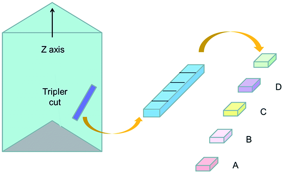 | ||
| Fig. 7 Schematic diagram of sample orientation relative to the crystal blocks. | ||
The experimental setup is illustrated in Fig. 8. The laser source was an Nd:YLF laser (1) with a wavelength of 1053 nm and a maximum output energy of 60 mJ. Part of the fundamental energy was transmitted to laser energy meter I (3) by the partial reflector (2) to monitor the stability of fundamental waves and normalize the results. The laser was transmitted to the ADP sample (5) after being frequency-doubled by a KDP doubler (4). The output laser was separated by a prism (7), and the 3ω laser was transmitted to laser energy meter II (8) to monitor the 3ω energy. A 532 nm diode-pumped laser (DPL) was used as the indicating laser. By tuning the optical stage (6) and recording the laser reflected on the scale paper (10), the angles of samples can be recorded.
 | ||
| Fig. 8 Experimental setup for measuring the 3ω conversion efficiency of ADP crystals. | ||
The laser energy meters were calibrated to ensure the accuracy of the data. The energy ratio of the doubled and fundamental laser was set to 2![[thin space (1/6-em)]](https://www.rsc.org/images/entities/char_2009.gif) :1 by tuning the KDP doubler.
:1 by tuning the KDP doubler.
Results and discussion
Transmittance
Fig. 9 shows the transmittance curves of ADP crystals. The transmittance of ADP grown with material B was higher than that of ADP grown with material A in the near-ultraviolet and near-infrared regions, while the transmittance of ADP grown with material A was higher than that of ADP grown with material B in the visible region. The variation in the visible region around 800 nm was attributed to the changing light source for the corresponding wave band. The samples were grown under the same conditions with materials of different purity. According to Table 1, material B had a higher purity than A. Consequently, we can conclude that the transmittance at most wavelengths can be increased by decreasing ionic impurities, particularly Fe3+ cations, in the starting material. Note that the ADP crystal possesses high transmittance in the ultraviolet range, which indicates its significant potential for application in FHG. | ||
| Fig. 9 Transmittance spectra of ADP crystals grown using different raw materials. | ||
Nonlinear optical coefficient
By fitting the experimental data (shown in Fig. 10), we determined the maximum values of the Maker fringe envelopes Im(0) to be 9.16 and 8.399 for ADP and KDP crystals respectively, corresponding to a nonlinear optic coefficients of 0.4701 and 0.39 pm V−1, respectively. The larger nonlinear coefficient of ADP accompanied by the similar growth characteristics indicated that ADP crystal is a promising alternative material for use in ICF.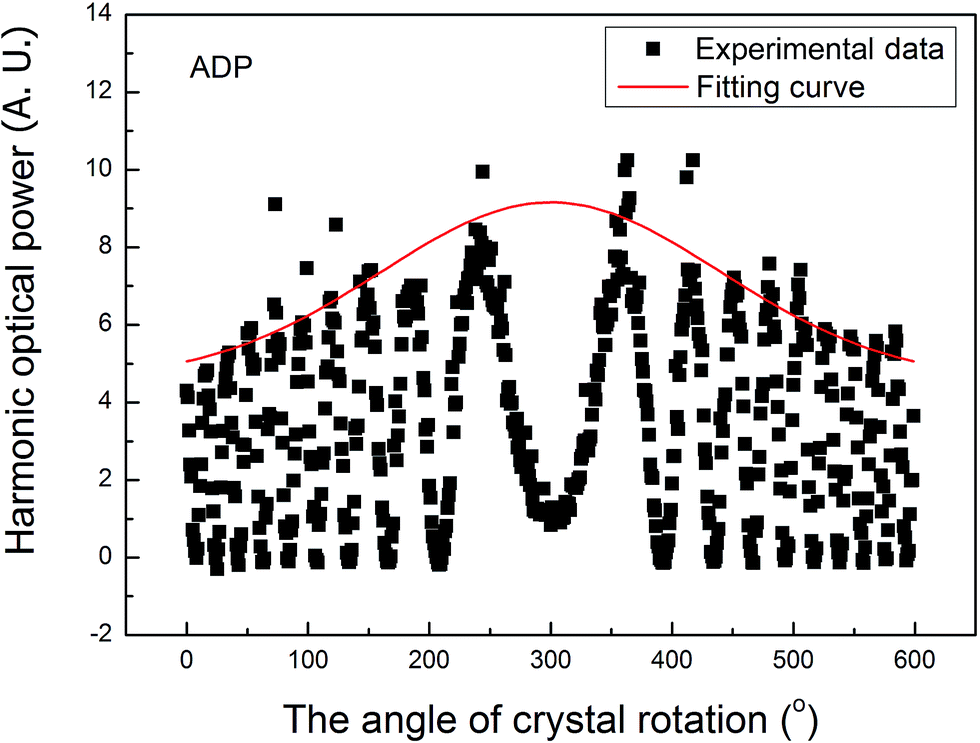 | ||
| Fig. 10 Maker fringe curves of ADP crystals. | ||
Laser-induced damage threshold
The THG laser damage thresholds are listed in Table 4; the normalized damage threshold of ADP was 2.5 times larger than that of 70% DKDP, and little difference was observed among the wafers possessing symmetrical growth positions and the same orientation and thickness.| LIDT (J cm−2, 7 ns) | Normalization LIDT (J cm−2, 3 ns) | Orientation (°) | Thickness (mm) | |
|---|---|---|---|---|
| 2–1 | 16.3 | 10.7 | 59 | 8.66 |
| 2–2 | 16.0 | 10.5 | 59 | 8.80 |
| 3–1 | 22.8 | 14.9 | 60 | 7.63 |
| 3–2 | 16.8 | 11.0 | 60 | 9.78 |
| 3–3 | 13.6 | 8.9 | 60 | 7.95 |
| 3–4 | 11.2 | 7.3 | 60 | 9.6 |
| 70% DKDP | 6.4 | 4.2 | 59 | — |
It can also be observed from the set of wafers 3–1 to 3–4 that the thinnest and farthest sample from the cap area 3–1 possesses the largest threshold, followed by the sample 3–2 which has a little larger thickness, while the samples with position next to the seed and in the recovery area 3–3 and 3–4 possess smaller threshold and the 8 mm thick one's threshold is larger than the 10 mm thick one's. Despite the difference sample set 3, all the ADP samples possessed larger thresholds than the 70% DKDP crystal, and the best one was 3.5 times larger. The analyses indicated that the growth area is a principal factor affecting the LIDT, while the thickness of the wafer also affects the result.
Third-harmonic generation
To determine the precise optimal phase-matching angle, we measured the angular bandwidth of samples under low energy intensity. The KDP samples were also tested under the same experimental conditions for comparison with ADP crystals. Fig. 11 shows that the ADP crystals from different positions and KDP crystal have little difference in angular bandwidth, which indicates that the growth position does not determine the angular bandwidth. | ||
| Fig. 11 Angular bandwidths of ADP and KDP crystals. | ||
The peak of each curve is where the highest THG conversion efficiency was obtained, corresponding to the precise optimal phase-matching angle.
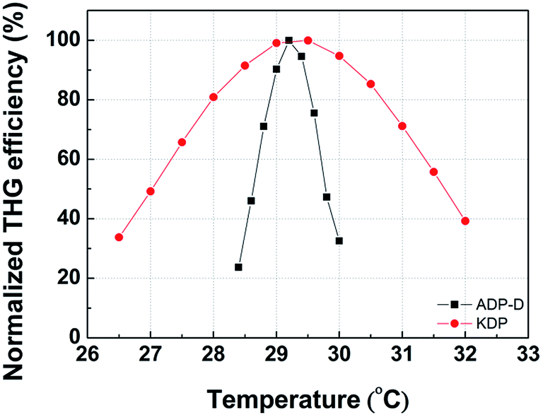
The temperature bandwidth of THG conversion efficiency is shown in Fig. 12. The conversion efficiency of KDP crystals remained >30% in the temperature range of 26.5–32 °C, while the temperature range for ADP crystals was 28.4–30.2 °C, indicating that ADP crystals require more stable conditions.
 | ||
| Fig. 12 Temperature bandwidths of ADP and KDP crystals. | ||
The ADP crystals' THG conversion efficiencies are shown in Fig. 13. The “1” in this figure refers to measurement without detuning the SHG, and the “2” refers to the measurement where the SHG crystal was detuned to obtain the phase-matching angle for high efficiency under high intensity. The THG conversion efficiency increased with the intensity of fundamental waves. Both crystals possessed conversion efficiencies higher than 50%, and detuning the SHG crystal had little effect on the efficiency.
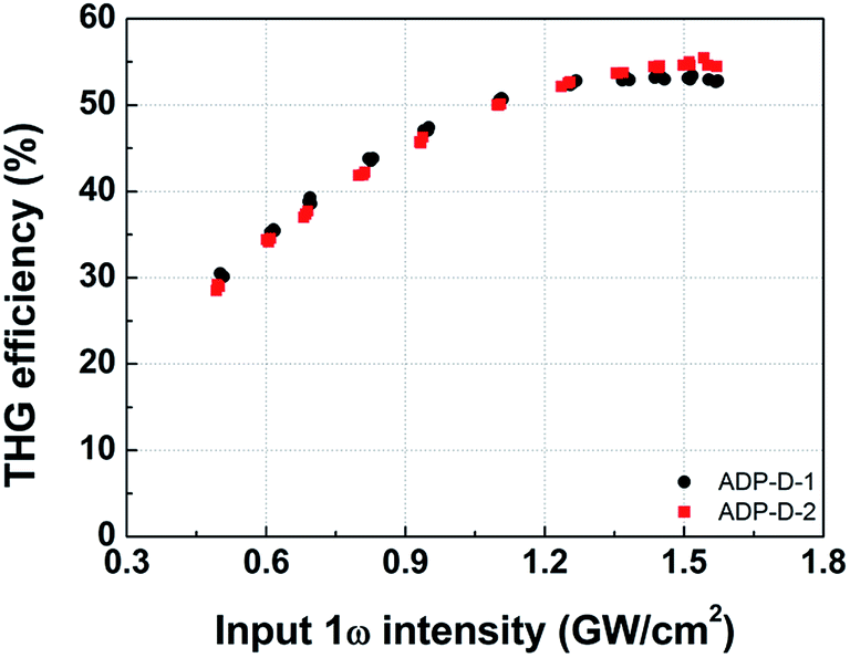 | ||
| Fig. 13 3ω conversion efficiencies of ADP triplers. | ||
The results of all five samples are compared in Fig. 14. All samples possessed efficiencies higher than 50%. Sample E's conversion efficiency was obviously lower than the others' under low intensity. Samples B and D possessed the highest efficiencies, and sample C's efficiency was slightly higher than that of sample A. Under a certain fundamental intensity, the difference between samples E and B and sample D reached 15%, which can be attributed to the different sample positions; samples B and D were positioned in a symmetrical location, while sample E was positioned on the edge area. These results suggested that the growth position significantly affects THG efficiency.
 | ||
| Fig. 14 3ω conversion efficiencies of different ADP triplers. | ||
Conclusion
The growth of ADP crystals and their optical properties, particularly THG, were systematically studied. A set of ADP crystals was grown using a temperature reduction method. First, an ADP seed crystal was obtained from a KDP seed crystal. Subsequently, a relatively large single ADP crystal was obtained using a Z-cut ADP wafer as a seed crystal. To solve the problem that the plate was hard to recover its cap wafer, a tetragonal pyramid was applied as the seed, and high-quality ADP crystals were finally obtained.In preparation for characterizing the frequency converting capability of the ADP crystals, various optical properties were tested. The transmittance test results suggested that the transmittance at most wavelengths can be increased by decreasing ionic impurities, particularly Fe3+ cations. The refractive indices were already reported in our earlier papers. The nonlinear optical coefficient of ADP crystal was measured to be 0.4701 pm V−1, larger than that of KDP crystal (0.39 pm V−1). The LIDT of ADP reached 3.5 times larger than that of DKDP. The growth area affected the LIDT significantly, while the thickness of the sample also influenced the results.
THG tests was performed systematically. The ADP crystal possessed the same angular bandwidth as the KDP crystal, but it was more sensitive to changes in temperature. Detuning the SHG crystal had little effect on the conversion efficiency. Sample position had a considerable effect on THG efficiency, but all samples exhibited efficiencies higher than 50%.
In conclusion, the results suggest that ADP crystals are a promising alternative to KDP crystals for ICF and other nonlinear applications.
Acknowledgements
This work was supported by the National Natural Science Foundation of China (Grant No. 61178060, 51323002 and 51402173), the Ministry of Education (Grant No. 625010360), Natural Science Foundation for Distinguished Young Scholar of Shandong Province (2012JQ18), and the Fundamental Research Funds of Shandong University (2015GN027). The Project 2014BB07 supported by NPL, CAEP is acknowledged.References
- J. A. Giordmaine, Phys. Rev. Lett., 1962, 8, 19 CrossRef.
- P. D. Maker, R. W. Terhune, M. Nisenoff and C. M. Savage, Phys. Rev. Lett., 1962, 8, 21 CrossRef.
- N. P. Zaitseva, J. J. De Yoreo, M. R. Dehaven, R. L. Vital, K. E. Montgomery, M. Richardson and L. J. Atherton, J. Cryst. Growth, 1997, 180, 255 CrossRef CAS.
- J. J. De Yoreo, A. K. Burnham and P. K. Whitman, Int. Mater. Rev., 2002, 47, 113 CrossRef CAS.
- L. Ji, B. Zhu, C. Liu, T. Wang and Z. Lin, Chin. Opt. Lett., 2014, 12, 031902 CrossRef.
- B. Liu, G. Hu, Q. Zhang, X. Sun and X. Xu, Chin. Opt. Lett., 2014, 12, 101604 CrossRef.
- Z. Li, X. Huang, D. Wu and K. Xiong, J. Cryst. Growth, 2001, 222, 524 CrossRef CAS.
- D. Eimerl, Ferroelectrics, 1987, 72, 95 CrossRef CAS.
- J. Reintjes and R. C. Eckardt, Appl. Phys. Lett., 1977, 30, 91 CrossRef CAS.
- D. A. Roberts, IEEE J. Quantum Electron., 1992, 28, 2057 CrossRef CAS.
- S. Ji, F. Wang, L. Zhu, X. Xu, Z. Wang and X. Sun, Sci. Rep., 2013, 3, 1605 Search PubMed.
- D. Xu and D. Xue, J. Cryst. Growth, 2006, 286, 108 CrossRef CAS.
- G. J. Linford, B. C. Johnson, J. S. Hildum, W. E. Martin, K. Snyder, R. D. Boyd, W. L. Smith, C. L. Vercimak, D. Eimerl and J. T. Hunt, Appl. Opt., 1982, 21, 3633 CrossRef CAS PubMed.
- R. J. Davey and J. W. Mullin, J. Cryst. Growth, 1974, 23, 89 CrossRef CAS.
- B. Žižić, R. J. Davey, S. Žegarac, T. Pastor, R. Ristić and M. M. Napijalo, J. Cryst. Growth, 1980, 49, 675 CrossRef.
- R. I. Ristic and J. N. Sherwood, J. Phys. D: Appl. Phys., 1991, 24, 171 CrossRef CAS.
- P. Rajesh and P. Ramasamy, Mater. Lett., 2010, 64, 798 CrossRef CAS.
- L. Zhu, B. Liu, L. Zhang, Q. Zhang, Z. Wang and X. Sun, Chin. Opt. Lett., 2015, 13, 041601 CrossRef.
- F. Zernike, J. Opt. Soc. Am., 1964, 54, 1215 CrossRef CAS.
- J. Jerphagnon and S. K. Kurtz, J. Appl. Phys., 1970, 41, 1667 CrossRef.
- M. Xu, X. Sun, Z. Wang, X. Cheng, S. Sun, L. Ji, Y. Zhao, B. Liu, H. Gao and X. Xu, Cryst. Res. Technol., 2010, 45, 763 CrossRef CAS.
- J. E. Swain, S. E. Stokowski, D. Milam and G. C. Kennedy, Appl. Phys. Lett., 1982, 41, 12 CrossRef CAS.
Footnotes |
| † Electronic supplementary information (ESI) available. See DOI: 10.1039/c6ra02283a |
| ‡ These authors contributed equally to this work. |
| This journal is © The Royal Society of Chemistry 2016 |