High performance oxygen-bridged N-shaped semiconductors with a stabilized crystal phase and blue luminescence

Chikahiko Mitsuia, Yuji Tanakab, Shota Tanakab, Masakazu Yamagishia, Katsumasa Nakaharac, Masafumi Yanob, Hiroyasu Satod, Akihito Yamanod, Hiroyuki Matsuia, Jun Takeyaac and Toshihiro Okamoto*ace
aDepartment of Advanced Materials Science, School of Frontier Sciences, The Univ. of Tokyo, 5-1-5 Kashiwanoha, Kashiwa, Chiba 277-8561, Japan. E-mail: tokamoto@k.u-tokyo.ac.jp
bFaculty of Chemistry, Materials and Bioengineering, Kansai Univ., 3-3-35 Yamate-cho, Suita, Osaka 564-8680, Japan
cThe Institute of Scientific and Industrial Research (ISIR), Osaka University, 8-1 Mihogaoka, Ibaraki, Osaka 567-0047, Japan
dRigaku Corporation, 3-9-12 Matsubara-cho, Akishima, Tokyo 196-8666, Japan
eJST, PRESTO, 4-1-8 Honcho, Kawaguchi, Saitama 332-0012, Japan

Received 12th January 2016 , Accepted 1st March 2016

First published on 2nd March 2016


Abstract

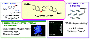
Here, we describe an oxygen-bridged N-shaped π-electron core, dinaphtho[2,3-d:2′,3′-d′]benzo[1,2-b:4,5-b′]difuran (DNBDF), as a new entity of organic semiconducting materials. Interestingly, by introduction of flexible alkyl chains at appropriate positions, DNBDF π-cores exhibit solution processability, a highly stabilized crystal phase, high mobility, and blue luminescence as a solid.


π-Electron systems composed of benzene- and/or heterole-fused π-electronic cores, especially, play an indispensable role in driving organic field-effect transistors (OFETs).1 For the creation of printed devices applicable to displays and radio frequency identifier (RFID) tags,2 the development of high performance organic semiconductors for OFETs is a crucial issue. In this context, a large number of promising materials with carrier mobility greater than that of amorphous silicon (0.5–1.0 cm2 V−1 s−1) were reported and investigated.3 One of the most important advantages of OFETs to be considered is their solution processability, allowing low-cost device fabrication. However, there is no straightforward way to develop practically applicable organic semiconductors featuring solution processability and a thermally stable aggregate form toward the device thermal durability, because they often result in trade-off relationships.4 To overcome this formidable challenge, we newly developed bent-shaped π-electronic cores with oxygen- and sulfur-bridged V-shaped π-conjugated molecules, dinaphtho[2,3-b:2′,3′-d]chalcogenophene (DNF–V and DNT–V, Fig. 1a).5 Indeed, sulfur-bridged derivatives (DNT–Vs) exhibit carrier mobility as high as 9.5 cm2 V−1 s−1, and a good device durability under thermal stress up to 150 °C.5a Moreover, we designed sulfur-bridged N-shaped molecules for π-electron expansion (Fig. 1b). Owing to their extended π-electron conjugation and zigzag shaped core structure, we successfully demonstrated that C10–DNBDT–NW exhibits excellent carrier mobility up to 16 cm2 V−1 s−1 in a solution-crystallized thin film. This OFET proved to be extremely robust against thermal stress, even at 200 °C.6 In this work, we focus on the oxygen-bridged N-shaped congeners, dinaphtho[2,3-d:2′,3′-d′]benzo[1,2-b:4,5-b′]difuran (DNBDF) derivatives, and elucidate their photophysical and thermal properties, aggregated structures and carrier transporting abilities. Notably, the incorporated chalcogen atoms have a significant impact on the electronic properties and aggregate structures, so that the emissive characteristics, thermal stabilities, as well as carrier transporting abilities are quite different among these molecules. Especially, by virtue of the light oxygen atom, previously developed DNF–Vs exhibit deep blue emission with a high quantum yield in the solid state, whereas the sulfur-containing congener, DNT–V, shows almost no emission. Such a high luminescence characteristic could be an additional fascinating feature toward the application of organic light-emitting transistors (OLETs).7 In this paper, we describe the syntheses of decyl group-substituted compounds at different positions (on the 2 and 10 positions: C10–DNBDF–NV; and on the 3 and 11 positions: C10–DNBDF–NW, Fig. 1b) together with the parent DNBDF and the effects of the substitution position on their thermal stability, solubility, photophysical properties, and carrier mobility in a thin film. Throughout this study, C10–DNBDF–NV exhibits a highly stabilized crystal phase up to 295 °C, blue emission with a moderately high quantum yield of 42%, even with flexible long alkyl chains in the solid state, and high carrier mobility up to 1.8 cm2 V−1 s−1 in a solution-crystallized FET, by taking advantage of its moderate solubility. This carrier mobility, determined by FETs, is considerably high among the hitherto developed furan-containing materials.8
image file: c6ra00922k-f1.tif
Fig. 1 Chemical structures of V- and N-shaped π-cores.

All of the DNBDF derivatives were synthesized utilizing the synthetic protocol, developed by us as illustrated in Scheme 1. Selective deprotonation of 2-methoxynaphthalene derivatives at the 3-positions, using n-BuLi, followed by transmetallation from lithium to zinc and Negishi cross-coupling with 1,4-dibromo-2,5-dimethoxybenzene in the presence of palladium catalyst afforded the coupling compounds 1a–c in high yields. Subsequent demethylation by boron tribromide gave the target precursors 2a–c. Finally, by use of a zeolite catalyst,5b,9 the dehydration smoothly proceeded producing the target compounds, which were finally purified by multiple recrystallization and vacuum sublimation. The synthesized DNBDF derivatives are pale green in the solid state, indicating the extension of the π-electron system, in comparison with the colorless DNF–V derivatives. Indeed, absorption spectrum measurements clarified that the absorption edge of DNBDF in a vacuum deposited thin film is 430 nm, which means a bathochromic shift by ca. 20 nm compared with DNF–V (Fig. S1). Due to the π-electron expansion, the ionization potential (IP) value of DNBDF in a vacuum deposited thin film on ITO, determined by photoelectron yield spectroscopy (PYS) measurements,10 is 5.70 eV, which is indeed smaller than that of DNF–V (5.93 eV). By introduction of alkyl chains in the DNBDF core, C10–DNBDF–NW and C10–DNBDF–NV exhibited smaller IP values of 5.67 eV and 5.65 eV, respectively, caused by their electron-donating nature (Fig. S4).


image file: c6ra00922k-s1.tif
Scheme 1 Synthesis of DNBDF derivatives.

We have studied the photophysical and thermal properties of DNBDF derivatives. The emission characteristics were investigated in both solution and solid. In solution, all three molecules exhibit blue emission with a high quantum yield of 65–78%. Even in a solid, DNBDF itself shows a high quantum yield of 71%. C10–DNBDF–NW and C10–DNBDF–NV show lower but moderate quantum yields of 36% and 42% due to the existence of flexible alkyl chains, respectively. Thermogravimetric analysis (TGA) showed a higher weight loss temperature (see Fig. S5). By heating the samples under a nitrogen gas atmosphere, the 5% weight loss temperatures (T95%) were determined to be 365 °C for DNBDF, 434 °C for C10–DNBDF–NW, and 420 °C for C10–DNBDF–NV, respectively. In contrast, V-shaped congeners, DNF–V, C10–DNF–VW, and C10–DNF–VV start to evaporate at lower temperatures with a T95% of 268 °C, 359 °C, and 365 °C. The higher weight loss temperatures of DNBDF derivatives are ascribed to their large molecular weight as well as the stronger dispersion energy between extended DNBDF π-cores. A remarkable substitution effect was observed in the stabilized crystal phase and solubility. Phase transition temperatures of the alkylated DNBDF were also measured by differential scanning calorimetry (DSC). It is noteworthy that the phase transition temperature from the crystal phase of C10–DNBDF–NW is just 104 °C, whereas that of C10–DNBDF–NV is significantly higher (295 °C) (Fig. S6). In comparison, the smaller V-shaped π-core derivatives, C10–DNF–VW and C10–DNF–VV, show a phase transition at 128 °C and 176 °C, respectively. Thus, the substitution at the 2,10 positions of the DNBDF core endows them with a thermally stabilized crystal phase. A solubility test was performed for these three compounds to choose the appropriate material for the fabrication of solution processed FETs. Although unsubstituted DNBDF is insoluble in 1,2,4-trichlorobenzene at 90 °C (less than 0.01 wt%), alkylated ones possess 0.037 wt% for C10–DNBDF–NW and 0.16 wt% for C10–DNBDF–NV in the same condition, respectively. These results suggest that both alkylated DNBDF compounds possess solution processability at a slightly high temperature.

In order to clarify the aggregate structures for understanding the carrier transporting ability using theoretical calculations, X-ray single crystal analyses were performed. All single crystals, grown by either horizontal physical vapour transport11,12 or the solution crystallization technique by gradient cooling, show platelet forms. X-ray structural analyses revealed that all DNBDF derivatives stack into a two-dimensional herringbone packing structure regardless of the presence and position of alkyl side chains (Fig. 2). For all DNBDFs, C–H short contacts were observed between the neighboring molecules attracted with the CH/π interaction, which could play the role of organizing the herringbone structures. This trend is quite different from the sulfur-bridged case. Actually, the DNBDT forms a slipped π–π stacking structure and thus exhibits a poor carrier mobility of 0.03–0.06 cm2 V−1 s−1 in single crystal FETs. Meanwhile, C10–DNBDT–NW, forming a two-dimensional herringbone packing structure, shows a carrier mobility as high as 16 cm2 V−1 s−1.6 (Note: C10–DNBDT–NV forms a different packing structure. The details on the packing structures and carrier transporting ability will be reported elsewhere.) We conjectured that the sterically less demanding oxygen atom and thus the larger obtuse angle of the DNBDF core enable all types of DNBDF derivatives to interact with each other by CH/π interaction and thus form herringbone packing structures, which are favourable for two-dimensional carrier transport. To quantitatively analyse their carrier transporting ability, band structure calculations were conducted based on the packing structure by way of a periodic boundary condition at the PBEPBE/6-31G(d) level (Fig. S8–11). In the band structures of DNBDFs, large band dispersion at the top of the valence band is observed in both directions in the conduction plane, indicating the potential of two-dimensional carrier transport. The calculated hole effective masses are inserted in Fig. 2.


image file: c6ra00922k-f2.tif
Fig. 2 Single crystal structures and effective masses of DNBDF derivatives.

The effective mass is inversely proportional to carrier mobility as described by the following equation: μ = /m* (μ: mobility, q: carrier charge, τ: relaxation time, m*: effective mass).13 Both alkylated DNBDFs possess almost the same hole effective masses in the transverse direction as that of C10–DNF–VW. Notably, they possess anisotropic values; that is, the effective masses in the transverse direction (m*) are much smaller than those in the columnar direction (m*) (Fig. 2). In contrast, unsubstituted DNBDF possesses larger effective masses, in both the columnar and transverse directions, than those of the alkylated ones. We assume that this is due to the unsubstituted DNBDF standing with a slightly tilted angle on the ab plane (the conduction plane). Thus, the introduction of a long alkyl side chain can finely tune the packing structures. Throughout the comprehensive investigation in terms of a stabilized crystal phase, solution processability, and carrier transporting capability, C10–DNBDF–NV proves to be the best candidate as a solution-processable OFET material in this study.

Finally, to clarify the carrier transporting capability, we fabricated OFETs with C10–DNBDF–NV in the form of single-crystalline films prepared by edge-casting, a solution-crystallization method originally developed by our group.14 A droplet of a 0.05 wt% hot solution of C10–DNBDF–NV in 1,2,4-trichlorobenzene at 120 °C was placed at the edge of a liquid-sustaining piece on a SiO2 substrate preliminarily treated with β-phenylethyltrichlorosilane (β-PTS).15 Along the direction of the solvent-evaporation at a substrate temperature of 90 °C, a large domain crystalline film formed on the substrate. On top of the prepared single-crystalline film, we made the contacts through a shadow mask to construct the channel in parallel to the crystal growth direction. Thus, a FET was fabricated by successive deposition of F4–TCNQ and the Au electrodes to construct the bottom-gate-top-contact architecture. The electron-accepting F4–TCNQ layer facilitates hole injection from the gold electrode.16 The FET of C10–DNBDF–NV operates as a p-type transistor with hole mobility up to 1.8 cm2 V−1 s−1 (1.3 cm2 V−1 s−1 on average among 10 devices; Fig. S13–17) and a threshold voltage of −90 V (Fig. 3). The molecular orientation and morphology of the obtained crystalline thin films were investigated by means of X-ray diffraction (XRD). The in-plane and out-of-plane XRD data for C10–DNBDF–NV revealed that the a-axis was oriented perpendicular to the substrate, and the bc plane was parallel to the substrate, where the film structure of C10–DNBDF–NV is desirable for 2D charge transporting (Fig. S18). Importantly, as the band calculation reveals, the crystal growth direction corresponds to the c-axis direction, in which this material shows a larger effective mass (m*/m0 = 6.4) compared to the b-axis direction (m*/m0 = 2.0). However, vertical to the highly conductive b-axis direction, some occasional cracks appear in the solution-crystallized film (Fig. S19). Therefore, to demonstrate the intrinsic carrier mobility, it is necessary to measure the FET in the b-direction after optimizing the crystal growth condition to avoid cracks.


image file: c6ra00922k-f3.tif
Fig. 3 (a) Transfer characteristics and (b) output characteristics of the typical transistor with the solution-crystallized C10–DNBDF–NV film.

In summary, we designed and synthesized DNBDFs, oxygen-bridged N-shaped materials for application in OFETs. In comparison with DNF–V derivatives, DNBDFs possess a smaller ionization potential and a higher weight loss temperature due to the π-extension. Notably, C10–DNBDF–NV exhibits a considerably high phase transition temperature of 295 °C and a moderately high photoluminescence quantum yield of 42% in the solid state. Single crystal analyses revealed that all DNBDFs synthesized in this study show a herringbone packing structure. Solution-crystallized thin film transistors using C10–DNBDF–NV show high hole mobility of up to 1.8 cm2 V−1 s−1. There is room to elevate the carrier mobility of this material by further optimizing the film growth process. Device thermal durability tests and applications of these materials in light-emitting devices are currently underway in our laboratory.

Acknowledgements

The authors thank Dr T. Suzuki and Mr T. Takehara for the XRD measurement of C10–DNBDF–NV in solution-crystallized thin film. C. M. thanks the JSPS Grant-in-Aid for Young Scientists (B) (No. 25810118). M. Y. thanks the JSPS Grant-in-Aid for Scientific Research (C) (No. 26410254) and the Kansai University Subsidy for Supporting Young Scholars, 2014. T. O. also thanks the JSPS Grant-in-Aid for Scientific Research (B) (No. 25288091). The authors thank the Comprehensive Analysis Center (CAC), ISIR, Osaka University for the measurement of the elemental analysis. This work was financially supported by JNC Petrochemical Corp. and JNC Corp., JAPAN.

Notes and references

  1. Z. Bao and J. Locklin, Organic Field-Effect Transistors, CRC Press, Florida, 1st edn, 2007 Search PubMed.
  2. (a) P. F. Baude, D. A. Ender, M. A. Haase, T. W. Kelley, D. V. Muyres and S. D. Theiss, Appl. Phys. Lett., 2003, 82, 3964 CrossRef CAS; (b) S. Steudel, K. Myny, V. Arkhipov, C. Deibel, S. De Vusser, J. Genoe and P. Heremans, Nat. Mater., 2005, 4, 597 CrossRef CAS PubMed.
  3. (a) J. E. Anthony, Chem. Rev., 2006, 106, 5028 CrossRef CAS PubMed; (b) C. Wang, H. Dong, W. Hu, Y. Liu and D. Zhu, Chem. Rev., 2011, 112, 2208 CrossRef PubMed.
  4. (a) J. Chen, J. Anthony and D. C. Martin, J. Phys. Chem. B, 2006, 110, 16397 CrossRef CAS PubMed; (b) H. Ebata, T. Izawa, E. Miyazaki, K. Takimiya, M. Ikeda, H. Kuwabara and T. Yui, J. Am. Chem. Soc., 2007, 129, 15732 CrossRef CAS PubMed.
  5. (a) T. Okamoto, C. Mitsui, M. Yamagishi, K. Nakahara, J. Soeda, Y. Hirose, K. Miwa, H. Sato, A. Yamano, T. Matsushita, T. Uemura and J. Takeya, Adv. Mater., 2013, 25, 6392 CrossRef CAS PubMed; (b) K. Nakahara, C. Mitsui, T. Okamoto, M. Yamagishi, H. Matsui, T. Ueno, Y. Tanaka, M. Yano, T. Matsushita, J. Soeda, Y. Hirose, H. Sato, A. Yamano and J. Takeya, Chem. Commun., 2014, 50, 5342 RSC.
  6. C. Mitsui, T. Okamoto, M. Yamagishi, J. Tsurumi, K. Yoshimoto, K. Nakahara, J. Soeda, Y. Hirose, H. Sato, A. Yamano, T. Uemura and J. Takeya, Adv. Mater., 2014, 26, 4546 CrossRef CAS PubMed.
  7. F. Cicoira and C. Santato, Adv. Funct. Mater., 2007, 17, 3421 CrossRef CAS.
  8. (a) O. Gidron and M. Bendikov, Angew. Chem., Int. Ed., 2014, 53, 2546 CrossRef CAS PubMed; (b) M. Watanabe, W.-T. Su, Y. J. Chang, T.-H. Chao, Y.-S. Wen and T. J. Chow, Chem.–Asian J., 2013, 8, 60 CrossRef CAS PubMed; (c) K. Oniwa, T. Kanagasekaran, T. Jin, M. Akhtaruzzaman, Y. Yamamoto, H. Tamura, I. Hamada, H. Shimotani, N. Asao, S. Ikeda and K. Tanigaki, J. Mater. Chem. C, 2013, 1, 4163 RSC; (d) O. Gidron, A. Dadvand, E. Wei-Hsin Sun, I. Chung, L. J. W. Shimon, M. Bendikov and D. F. Perepichka, J. Mater. Chem. C, 2013, 1, 4358 RSC; (e) K. Niimi, H. Mori, E. Miyazaki, I. Osaka, H. Kakizoe, K. Takimiya and C. Adachi, Chem. Commun., 2012, 48, 5892 RSC; (f) C. Mitsui, J. Soeda, K. Miwa, H. Tsuji, J. Takeya and E. Nakamura, J. Am. Chem. Soc., 2012, 134, 5448 CrossRef CAS PubMed; (g) M. Nakano, H. Mori, S. Shinamura and K. Takimiya, Chem. Mater., 2011, 24, 190 CrossRef; (h) O. Gidron, A. Dadvand, Y. Sheynin, M. Bendikov and D. F. Perepichka, Chem. Commun., 2011, 47, 1976 RSC; (i) Y. Miyata, M. Terayama, T. Minari, T. Nishinaga, T. Nemoto, S. Isoda and K. Komatsu, Chem.–Asian J., 2007, 2, 1492 CrossRef CAS PubMed.
  9. A. Arienti, F. Bigi, R. Maggi, P. Moggi, M. Rastelli, G. Sartori and A. Trere, J. Chem. Soc., Perkin Trans. 1, 1997, 1391 RSC.
  10. M. Honda, K. Kanai, K. Komatsu, Y. Ouchi, H. Ishii and K. Seki, Mol. Cryst. Liq. Cryst., 2006, 455, 219 CrossRef CAS.
  11. R. A. Laudise, C. Kloc, P. G. Simpkins and T. Siegrist, J. Cryst. Growth, 1998, 187, 449 CrossRef CAS.
  12. For preparation of single crystals of DNBDF, horizontal physical vapor transport technique was applied. The length and diameter of Pyrex tube used are 120 cm and 2 cm, respectively. Under Ar carrier gas flow as a flow rate of 50 ccm, source and crystallization-zone temperature were maintained at 350 °C and 260 °C, respectively.
  13. M. C. R. Delgado, E.-G. Kim, D. A. d. S. Filho and J.-L. Bredas, J. Am. Chem. Soc., 2010, 132, 3375 CrossRef PubMed.
  14. T. Uemura, Y. Hirose, M. Uno, K. Takimiya and J. Takeya, Appl. Phys. Express, 2009, 2, 111501 CrossRef.
  15. T. Umeda, D. Kumaki and S. Tokito, J. Appl. Phys., 2009, 105, 024516 CrossRef.
  16. T. Minari, T. Miyadera, K. Tsukagoshi, Y. Aoyagi and H. Ito, Appl. Phys. Lett., 2007, 91, 053508 CrossRef.

Footnote

Electronic supplementary information (ESI) available. CCDC 1400149–1400151. For ESI and crystallographic data in CIF or other electronic format see DOI: 10.1039/c6ra00922k

This journal is © The Royal Society of Chemistry 2016
Click here to see how this site uses Cookies. View our privacy policy here.