rGO-Wrapped flowerlike Bi2Se3 nanocomposite: synthesis, experimental and simulation-based investigation on cold cathode applications

Biswajit Dasa, Samrat Sarkara, Rimpa Khana, Saswati Santrab, Nirmalya Sankar Dasa and Kalyan Kumar Chattopadhyay*ab
aSchool of Materials Science & Nanotechnology, Jadavpur University, Kolkata 700 032, India. E-mail: kalyan_chattopadhyay@yahoo.com; Fax: +91 33 2414 6007; Tel: +91 9433389445
bThin Film & Nanoscience Laboratory, Department of Physics, Jadavpur University, Kolkata 700 032, India

Received 30th December 2015 , Accepted 25th February 2016

First published on 26th February 2016


Abstract

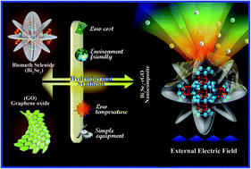
Bi2Se3 nanoflowers (NFs) and reduced graphene oxide (rGO) nanocomposite (BG) have been synthesized by a cost-effective, ecofriendly and easy hydrothermal route for the first time. Thorough characterizations confirm the phase, chemical composition and morphology of the samples. Room temperature transport measurement showed that the composite samples exhibit enhanced electrical conductivity compared to the pure Bi2Se3 nanoflowers (NFs). The possibility of using this composite in applications such as low macroscopic field emitters for cold cathode application has been investigated. For this, theoretical simulations are performed for pure and composite samples with graphene wrapping of different degrees and to evaluate the relation between the degree of rGO wrapping and the enhancement of FE properties, and the same was verified experimentally. It is observed that the enhancement factor for cold cathode emission of Bi2Se3–rGO (BG) composite is almost 5 times higher than that of pristine GO, 2.6 times that of rGO and nearly 1.5 times higher than that of pure Bi2Se3 NFs. The enhancement of the cold emission properties is attributed to suitable wrapping of rGO sheets over Bi2Se3 NFs. This produces more curvature at the nanoflakes edges and the electron affinities between the materials are favorable for the enhancement of cold cathode emission. The sample exhibiting the best FE properties also showed photoresponse properties under visible light excitation.


1. Introduction

Structural modification in the nano-domain has emerged as an effective technique to enhance electrical and optical properties of a wide range of materials in recent years.1–4 Considerable efforts have been devoted for assembling these types of advanced nanostructured materials for developing ‘multipurpose’ materials.5,6 Recently 2D nanostructures of carbon allotropes have drawn much attention due to their ever-blooming advanced applications. Several investigations on transport,7 luminescence8 and field emission9 properties of graphene and related materials have been performed. Reduced graphene oxide (rGO) is composed of few layer sp2 bonded carbon atoms arranged in a honeycomb like lattice.10 Synthesis and functionalization of rGO using low cost solution method11,12 have shown high yield of production. Considering the possibilities to obtain a new class of multifunctional hybrid materials, rGO based composites have drawn much scientific and technological interests during the last decade.5,13,14 For example, different metal and semiconducting nanoparticles decorated on graphene oxide (GO) have been reported for novel catalytic,15 electric,16 magnetic17 and photoresponse18 properties.

In this regard, we propose bismuth selenide (Bi2-Se3) as a potential candidate, among many metal chalcogenides,19,20 for composite formation with 2D carbon nanostructures. Bi2-Se3 is a well-known low band gap (∼0.3 eV) material.21,22 Additionally a unique property, namely topological insulating behavior has been observed23–25 in Bi2Se3 which enables its bulk insulating states encapsulated by conducting surface states. Coupling between spin and orbit in such materials is strong26–29 enough to generate intercross band structure and provides conducting surface states by locking the orientations of spin and momentum of the electrons during their propagation at opposite directions.30,31 In our previous report we exploited these properties of Bi2Se3 and showed topological surface state protected efficient field emission from Bi2Se3–Ag32 hybrid system.

Careful analysis of the mentioned optoelectronic properties of graphene and Bi2-Se3 strongly indicates the feasibility of formation of efficient nanocomposites involving these two novel materials. Both Bi2Se3 and rGO exhibit single Dirac cone on their surfaces19,33 facilitating easy charge transfer. Both of them have identical layered structures34 minimizing the possibility of lattice mismatch which is a key factor for proper composite fabrication. Strong spin orbital coupling28 exhibited by Bi2Se3 favors attachment of rGO sheets on its surface. Moreover, Bi2Se3 NFs prepared in previous works32 exhibited lesser number of sharp emitting edges which may be increased by introducing graphene wrinkles upon its surface. Additionally, rGO, being an appreciably conducting material, is expected to exhibit very high emission current density whereas Bi2Se3 NFs should offer a considerably low turn-on field due to their high aspect ratio. Combination of these two is therefore expected to result interesting and very efficient cold emission applications. In spite of such possibilities Bi2Se3–rGO hybrid systems have been rarely investigated35–37 and further research in this aspect must be carried out.

Triggered by this idea, here we report for the first time a simple and cost effective chemical route to synthesize binary Bi2Se3/rGO (BG) composite nanostructures. Choosing the proper route for composite fabrication often governs the behavior of the composite. The nature of surface of the host material is another crucial factor regarding this. There are contradictory reports regarding the surface activity of Bi2Se3; some research groups38 claim that poorly protected surface states of Bi2Se3 often suffers local surface oxidation during any surface activity, whereas others claim that surface states of Bi2Se3 are stable29 against mild environmental agents. During composite fabrication, both the factors were taken care of as it cannot be conclusively stated which of the above features will be dominant in the Bi2Se3 samples, especially in nano regime. If the surfaces are not active enough, attachment of the wrapping material to fabricate proper composite might be difficult and hence harsh chemical treatment would be inevitable. On the other hand, if Bi2Se3 NFs exhibit unprotected surface states, there is considerable risk of damage of the host material due to such stringent chemical treatment leading to inferior properties of resulting composite. This challenge was efficiently solved by employing hydrothermal route using prefabricated Bi2Se3 NFs and GO as precursors. This technique is free from harsh chemical treatment for reduction of GO and carried out within a properly closed vessel minimizing the possibilities of chemical damage from other precursor or external reagents. Additionally the auto generated pressure within the hydrothermal vessel ensures the wrapping of rGO sheets irrespective of active or inactive nature of the surface of the host Bi2Se3 NFs. Exploiting these facilities, unlike previous reports35–37 we have successfully wrapped the Bi2Se3 nanostructures with 2D graphene sheets rather than forming mere layered structures in order to allow better charge exchange and achieve enhanced properties. As the nature of wrapping, i.e. effective surface area of the NFs actually covered by rGO sheets can play a crucial role in tuning the behavior of the composite, different synthesis durations were maintained to achieve different degree of rGO wrapping over Bi2Se3 NFs. The presence of rGO layers on flower like Bi2Se3 helps to incorporate low screening effect, high electron density, increase electron emitting sites and thermal stability. This is reflected in enhanced field emission performance of the hybrid system compared to pristine GO and Bi2Se3 NFs. The presence of sharp edges, wrinkles, defects and dislocations of rGO layers on topological insulator nanostructure improves the quantity of surface electrons which is accounted for the enhancement of cold emission properties of the resultant nanocomposite. Moreover, wrapping by rGO layer is expected to influence the absorbance of visible light by the composite system compared to the pristine Bi2Se3 NFs which may be used to enhance the photoinduced transport properties.

2. Experimental

Materials synthesis

All the chemical reagents used in this study are of analytical grade and used as received without further purification. All aqueous solutions are prepared with deionized (DI) water.

Synthesis of Bi2Se3 nanoflowers (NFs) and graphene oxide (GO)

The detailed synthesis methods of pure Bi2Se3 NFs39,40 and GO are described in the ESI 1.

Synthesis of Bi2Se3 NFs/rGO composite (BG)

Hydrothermal method was employed to synthesize the Bi2Se3 NFs/rGO composite. 30 mg of as-prepared Bi2Se3 NFs was added to the 30 ml of as synthesized homogeneous GO solution and stirred in a magnetic stirrer for 2 h until a uniform suspension was formed. The suspension was then poured into a Teflon-lined stainless steel autoclave of 50 ml capacity which was maintained at 180 °C for different time durations of 10 h, 15 h and 20 h under auto generated pressure to synthesize the composite of Bi2Se3 NFs/rGO (denoted as BG). Reduction of GO was also realized during this process.40 After cooling down to room temperature, the product was collected as residue after filtration and the same was washed several times with DI water and dried at ambient conditions to obtain the final product. The samples synthesized during 10 h, 15 h and 20 h were labeled as BG10, BG15 and BG20 respectively. The general synthesis process is stepwise demonstrated schematically by Fig. 1.
image file: c5ra28064h-f1.tif
Fig. 1 Stepwise flowchart of the synthesis of Bi2Se3–rGO nanocomposite.

Characterizations

The phase purity and crystallinity of the as-synthesized Bi2Se3 NFs and BG composites were investigated by a X-ray diffractometer (Bruker D8 Advanced) with Cu Kα radiation (λ = 1.54056 Å, operating at 40 kV and 40 mA) in a 2θ range from 15–70°. The morphologies and microstructures of the samples were examined using field emission scanning electron microscopy (FESEM, Hitachi S-4800) at an accelerating voltage of 5.0 kV. The chemical compositions as well as the spatial uniformity of the elemental distribution were analyzed by the energy dispersive X-ray spectroscopy (EDS, Thermo Scientific attached with Hitachi S-4800) operated at 15.0 kV. High-resolution transmission electron micrographs (HRTEM) as well as selected area electron diffraction (SAED) images were taken by a JEOL 2010 TEM operating at an accelerating voltage of 200 kV. Room temperature Raman spectra was recorded using Raman spectrometer (alpha 300, Witec, Germany, laser source of λ = 532 nm). Fourier transformed infrared spectroscopic (FTIR, Shimadzu-8400S) analysis revealed the bond information for stretching vibrational modes of GO and BG20 composite. Electrical conductivity of the pristine Bi2Se3 NFs and Bi2Se3 NFs/rGO (BG20) composite samples were measured using standard method, for this the samples were spin coated within the gap between an ITO strip on a glass substrate and silver contacts were made from the ITO. The same experiment was repeated under visible light illumination to investigate any possible enhancement in photoresponse behavior. The possible relation of emission behavior of the samples with degree of wrapping of rGO sheets was established via theoretical simulations using ANSYS MAXWELL software. Considering the outcome of theoretical simulations, BG20 was inferred as the most efficient emitter and the same was characterized for FE properties experimentally. The field emission properties of the pristine GO, Bi2Se3 NFs and composite BG20 were studied inside our laboratory made high vacuum chamber with a diode configuration setup. The nanostructure powders spread over a carbon tape were considered as the cathode and a stainless steel conical tip with diameter ∼ 1 mm as an anode and the inter electrode distance was kept ∼180 μm with high precision by means of a micrometer screw. The whole surface of the sample was visible through a chamber view port to observe whether any discharge was occurring. No such discharge was found during the measurement which ensured that the samples exhibit cold electron emission.

3. Results and discussion

Morphology and structure

The phase identification of pure Bi2Se3 NFs and BG composite with highest degree of rGO wrapping, i.e. BG20, was performed by X-ray diffraction. The powder XRD patterns confirmed the structural characteristic and phase composition of the samples were illustrated in Fig. 2. It is clear that both the samples possess similar XRD peaks. All the diffraction peaks of pure Bi2Se3 NFs can be matched with the orthorhombic Bi2Se3 lattice (JCPDS card no. 33-0214). In addition, one typical diffraction peak of rGO (002)17 has been observed in the XRD pattern of the BG composite. The microstrain within the lattice of host Bi2Se3 NFs were determined using the well-known Williamson–Hall formula32 (not shown here) and no considerable increase in lattice strain was observed even within BG20. This indicates proper matching of lattices between the counterparts which is favorable for stability of the composite form.
image file: c5ra28064h-f2.tif
Fig. 2 X-Ray diffraction patterns of Bi2Se3 nanoflowers and composite BG20.

The morphological characteristics of the as synthesized Bi2Se3 NFs, GO and all the samples BG10, BG15 and BG20 of BG composites were studied by FESEM. The investigations were aimed in two directions. Firstly, it was studied whether the rGO sheets wrapped over Bi2Se3 NFs identically for different synthesis durations. The results are depicted in Fig. 3. Fig. 3(a and b) show the low and high magnification images of Bi2Se3 NFs treated for 10 h in hydrothermal chamber (i.e. BG10). In both the figures it can be easily seen that a very tiny sheet of rGO is present over the Bi2Se3 NFs leaving larger portion of the same uncovered. Fig. 3(b) shows it more specifically, that the rGO sheets, being rare in occurrence are mere coexisting along with the Bi2Se3 NFs rather than wrapping or covering them. The situation enhanced considerably in case of BG15 as depicted in Fig. 3(c and d), the rGO sheets are increased in area and hence could cover comparatively larger amount of Bi2Se3 NFs than in case of BG10. The wrapping by rGO sheets turned ‘global’ in nature in case of BG20 as can be found in Fig. 3(e) where almost the entire pack of Bi2Se3 NFs are properly covered by rGO sheets. The higher magnification image presented in Fig. 3(f) clearly indicate that the rGO sheet is not just existing as a covering layer upon the Bi2Se3 flower as a whole, rather it wrapped over the constituent individual Bi2Se3 nanoflakes. Hence form morphological studies by FESEM, we could infer that most effective and large area wrapping of rGO sheets on Bi2Se3 nanostructures were achieved for BG20, i.e. for 20 h hydrothermal duration. This can be accounted for the fact that we have taken sufficient amount of precursors for rGO preparation in hydrothermal reduction but the reaction is time consuming.41 In case of BG10, very little amount of GO solution is reduced to form rGO due to insufficient synthesis time. As the synthesis time increased larger amount of GO solution could reduce in rGO sheets and attached over the Bi2Se3 NFs and achieved most proper form in case of BG20 (Fig. 3(e and f)).


image file: c5ra28064h-f3.tif
Fig. 3 FESEM images of Bi2Se3–rGO composites in high and low magnification for (a and b) BG10; (c and d) BG15 and (e and f) BG20.

The second goal of our morphological studies was to investigate the details of nature of wrapping and comparative representation of the pristine and best wrapped Bi2Se3 NFs (BG20). The results are summarized in Fig. 4. In Fig. 4(a and b) we can see the pure rGO sheets in different dimensions, the wrinkles are clearly visible in Fig. 4(b). The pristine Bi2Se3 NFs were found to be of dimension of ∼1.5–2.00 μm as can be estimated from Fig. 4(c) and individual nanoflakes have average thickness of ∼20 nm (Fig. 4(d)) which indicates a very high aspect ratio of the Bi2Se3 NFs. Again in BG20, the maximum amount of Bi2Se3 nanostructures get properly covered with rGO sheets as depicted in Fig. 4(e) again, Fig. 4(f) shows that individual Bi2Se3 NFs are properly wrapped and even the wrinkles of rGO sheets can be visible over the surface of the Bi2Se3 nanoflakes (Fig. 4(f)).


image file: c5ra28064h-f4.tif
Fig. 4 Low- and high-magnification FESEM images of (a and b) pristine GO; (c and d) Bi2Se3 nanoflowers with large area image in inset of (c) and (e and f) rGO wrapped Bi2Se3 NFs composite BG20.

The special existence and degree of partial wrapping of rGO observed from FESEM studies was again verified using chemical mapping of constituent elements in BG10, BG15 and BG20 before choosing any particular sample for application based characterization. The results are presented in Fig. 5. It can be easily seen that spatial homogeneity as well as density of the elements of host Bi2Se3 NFs, i.e. Bi and Se are almost identical for each samples as represented in Fig. 5(a–c, e–g and i–k). However, the distribution and density (indicated by green colour) of elemental carbon, which is the sole representative of wrapping rGO layer, is varied appreciable from BG10 to BG20. BG10 shows rare presence of carbon (Fig. 5(d)) which became denser in BG15 (Fig. 5(h)). The homogeneity of green colour representing the spatial distribution of carbon (Fig. 5(l)) in case of BG20 is almost identical to that of Bi and Se (Fig. 5(j and k)). These results eventually reinforce our inference that BG20 being treated within the hydrothermal chamber for sufficient duration, possess largest amount of rGO sheets wrapped over the Bi2Se3 NFs which is reflected by the appreciable (and comparable to that of Bi and Se) distribution of elemental carbon within the sample. Two more important quantitative results regarding stoichiometric composition of the samples were obtained from EDX studies and the same are summarized in Fig. 6. Firstly, the stoichiometric ratio of the host elements Bi and Se are close to their expected values and remained almost same in pristine form and even in BG20 which had undergone hydrothermal treatment for longest duration.


image file: c5ra28064h-f5.tif
Fig. 5 Micrograph image and corresponding EDX elemental mapping showing the distribution of constituent elements (Bi, Se and C) for (a–d) BG10; (e–h) BG15 and (i–l) BG20.

image file: c5ra28064h-f6.tif
Fig. 6 (a and b) Atomic percentage before and after composite formation of (a) elemental Bi; (b) elemental Se and (c) corresponding EDX spectra of pure Bi2Se3 and composite BG20.

On the other hand, from EDX studies of sample C, the C/O ratio of BG composite was found to be ∼8.7 which is close to the value for conventional rGO.42 These observations are important in order to establish the novelty of the technique for composite formation in our work. As we mentioned in introduction section, using GO and Bi2Se3 for hydrothermal treatment instead of choosing both pre-synthesized Bi2Se3 NFs and rGO, ensured proper attachment and composite formation rather than production of simple mixture of the counterparts. In addition to that as, no strong chemical reagents were used for hydrothermal treatment, the stoichiometric ratios of the elements within the host material and the wrapping rGO were maintained in their expected values which is a notable success of this technique of composite fabrication.

However, as the dimension and carrier exchange play important role in modifying the properties of the composite material, we carried out HRTEM analysis of pristine GO, Bi2Se3 NFs and composite BG20 to find out the actual size of the involved counterpart and nature of interaction in between them. The obtained micrographs are shown in Fig. 7. We can see that the pure rGO sheets are few square micrometers in area (Fig. 7(a)) having traditional wrinkles within it (Fig. 7(b)) and few layer thick (Fig. 7(c)) which was later used to wrap over a large portion of Bi2Se3 NFs. The well known hexagonal pattern of diffraction spots can be observed within the SAED pattern of the same indicating good crystallinity of rGO. Transparent Bi2Se3 nanoflakes (Fig. 7(e)) and a considerable roughness at the edges of the flakes (Fig. 7(f)) were also observed from TEM study with a distinct and sharp lattice image of (015) plane of the same (Fig. 7(g)) proves proper crystallinity of the synthesized Bi2Se3. The SAED pattern obtained for Bi2Se3 NFs are presented in Fig. 7(h) shows several concentric intense hexagonal diffraction spots indicating multi stacked Bi2Se3 flakes with very good crystallinity. The most important micrographs are presented in Fig. 7(i and j) where the proper wrapping of the two counterparts are shown in both planar and normal view. The lattice fringes of Bi2Se3 NFs were found to be lying at very close proximity of the rGO layers as depicted in Fig. 7(k) and in the inset of the same ensuring the possibility of easy carrier exchange in between the two counterparts. The lattice image of BG20 (Fig. 7(l)) shows that the faint hexagonal diffraction pattern (the innermost of which is indicated by yellow bordering) of rGO to be completely superimposing with the hexagonal diffraction spots of Bi2Se3 NFs confirming the least lattice mismatch in between rGO and Bi2Se3. This is in full agreement with our XRD results where no considerable deviation of Bi2Se3 diffraction peaks from standard data was observed and studied.


image file: c5ra28064h-f7.tif
Fig. 7 Low and high magnification TEM images; HRTEM and SEAD patterns of (a–d) GO sheet; (e–h) pure Bi2Se3 nanoflake and (i–l) Bi2Se3–rGO composite BG20.

Raman and FT-IR spectroscopy

Room temperature Raman spectra of the as prepared samples were obtained using laser excitation of 532 nm. The spectra of the as synthesized GO and BG20 composite after hydrothermal reduction were shown in the Fig. 8(a). Two characteristic peaks at about 1350 cm−1 and 1597 cm−1 can be assigned to the documented D and G band of graphene respectively.17 The D band is related to the vibrations of sp3 carbon atoms which signify the structural defects and the disorder inside the graphene oxide nanosheets, and the G band corresponds to vibrations of sp2 carbon domains. The intensity ratio (ID/IG) of the D band to the G band is related to the average size of the sp3 domains over sp2 domains. Higher the intensity ratio of (ID/IG)15 signify the smaller the sp2 domains. Here the ID/IG ratio (1.03) of BG composite is higher than that (0.872) of graphene oxide. The significant increase in the value of ID/IG ratio can be explained by two ways. Firstly, an increase in the value of ID is due to the increase in structural defects and disorder after the hydrothermal treatment. Secondly, there is restoration of sp2 carbon in the graphene lattice and correspondingly the decrease in size of the sp2 domains due to the incorporation of H atoms in the system. This contribute to the decrease in the value of IG while reduction of GO to rGO. Thus the increase in the value of ID/IG ratio suggests that after the hydrothermal process the GO in the composite has been deoxygenated and reduced to rGO.
image file: c5ra28064h-f8.tif
Fig. 8 (a) Raman spectra and (b) FT-IR spectra of GO and Bi2Se3–rGO composite BG20.

In order to verify the formation of BG composites, the samples were investigated using FI-IR spectroscopy and the spectra were shown in Fig. 8(b). In the GO spectra the broad absorption band at 3343 and 1433 cm−1 originate from the stretching vibration and deformation vibration of OH. Other characteristic bands due to the stretching vibration of C[double bond, length as m-dash]O at 1731 cm−1 and C–O at 1032 cm−1 were also observed.17 The spectrum of GO shows an absorption peaks at 1631 cm−1 which is due to the stretching vibration of the sp2 hybridized C[double bond, length as m-dash]C bond and sp3 hybridized C–C bond at 1114 cm−1, which signify the presence of functional groups in the GO. However, after hydrothermal process, the oxygen-containing functional bonds were decreased dramatically which can be gauged by comparing the FT-IR spectra of GO and BG20 composite system. Moreover, the characteristic peaks of rGO nanosheets are usually recognized to be arising due to asymmetric stretching of CH2 at 2920 cm−1 and the symmetric stretching of CH2 at 2859 cm−1 (ref. 43) at the edge defects which is increased in case of composite system.

Electrical conductivity analysis

Room temperature electrical transport properties were analyzed using standard method to investigate whether and change of electrical conductivity occurs due to composite formation. The obtained result is presented in Fig. 9(a). We can see that the composite samples exhibit better conductivity than pristine Bi2Se3 NFs. The result may be accounted for the carrier exchange between highly conducting rGO layers and Bi2Se3 NFs which in turn increased the conducting feature of the composite. This result was further correlated with the enhancement of electrical field emission properties of BG20 (discussed later). Liu et al.44 theoretically had shown the band structure of similar system and calculated the minimum band gap at Γ point for Bi2Se3/graphene which are lower than the pristine Bi2Se3. They suggested that the better conductivity of the BG composite may be accounted for the lowering of band gap after composite formation which is strongly in agreement with our experimental outcome. Similar phenomenon was observed by Qiao et al.45 in their study with Bi2Te3.
image file: c5ra28064h-f9.tif
Fig. 9 (a) Room temperature IV characteristics of pure Bi2Se3 and Bi2Se3–rGO composite BG20 (inset showing the arrangement for measurement) and (b) photoresponse properties of BG20 under visible light illumination.

Fig. 9(b) shows the photoresponse properties exhibited by sample BG20. We can see a considerable increment of output current under visible light illumination than under dark condition. This result can be accounted for the absorbance of the composite system. As rGO is a well known absorbent of visible light, the effective absorbance within visible range increases in case of BG20 which in turn emphasized the influence of the incident illumination and caused higher output current under the exposure.

ANSYS analysis

To investigate the effect of the morphology of Bi2Se3 NFs and origin of high current density after attachment of rGO nanosheets with it, the electrostatic field distribution was simulated based on the finite element method with ANSYS Maxwell simulation software.32 The 2D electric field distributions were theoretically calculated for Bi2Se3 NF and rGO wrapped Bi2Se3 NF based cathodes. The dimensions used for modeling of those nanostructures were considered as per actual basis and in accordance to FESEM and TEM results. Electrode separation, type of the collector etc. were kept as the actual experimental parameters. As we have postulated that the degree of wrapping of rGO affects the behavior of the resulting BG composite, we have theoretically modeled rGO layers wrapping over Bi2Se3 NF and increased the amount of wrapping step by step. Each model was compiled individually and the simulation was repeated for each degree of wrapping to estimate whether any change of the emission electric field, in terms of distribution or magnitude, can at all be predicated. The obtained results of simulation are shown in Fig. 10. We can see that the electric field distribution and its magnitude gradually increase as we increase the degree of wrapping of rGO over Bi2Se3 NF models and the composite system emits maximum field when rGO wrapping is maximum (Fig. 10(e and j)) which is analogous to our experimental BG20. The same is reflected even when we considered arrays of composite models in place of a single emitter (Fig. 10(k and l)). It was also checked theoretically whether the enhanced emission can be contributed solely by rGO sheets. For this rGO sheet of thickness 10 nm was modeled. The values of bulk conductivity and relative permittivity required as input parameters for ANSYS simulation was considered identical to those of the ideal rGO so that the model can show best possible emission field which will be essential to predict whether rGO sheet can on its own emit enhanced electric field as high as emitted by the composite model. The results are depicted in Fig. 10(m and n) which show that rGO sheets, even of best quality, is not expected to be able to emit high electric field compared to composite model, neither such a high emission field density can be achieved using pure Bi2Se3 NF models (Fig. 10(a and f)). This outcome of simulative calculation was further verified by actual experiment using pure GO, pristine Bi2Se3 NFs and composite BG20 which is analogous to the composite model showing best emission.
image file: c5ra28064h-f10.tif
Fig. 10 Simulated electric field distribution of (a–e) single composite nanostructure with 0–4 number of wrapping rGO layers respectively in side view; (f–j) corresponding top views; (k) array of Bi2Se3 NFs in side and top view wrapped by 0 rGO layers; (l) array of Bi2Se3 NFs in side and top view wrapped by 4 rGO layers; pure rGO layer in (m) side and (n) top view.

Field emission (FE) properties

The Field Emission (FE) properties of the pristine GO, rGO, Bi2Se3 NFs and composite BG20 were investigated using a diode setup at room temperature. The emission current density observed due to cold emission from various samples are depicted in Fig. 11(a) by a plot of the emission current density (J) as a function of the applied electric field (E) at an anode-sample distance of 180 μm inside a high vacuum chamber (∼10−6 mbar). We can clearly observe that the emission current density of GO is not at all appreciable as it is expected. The very high emission current density was for pristine Bi2Se3 NFs was attributed to their high aspect ratio as obtained from FESEM result (Fig. 4(d)). However, the emission current density was further increased and reached a very high value (∼1.1 mA cm−2) for composite BG20, where proper composite was formed and rGO wrapping over Bi2Se3 NFs was observed (Fig. 5(l)) at almost entire region. The highest current density that was obtained in case of BG composite is around 8, 4 and 1.6 times greater than GO, Bi2Se3 NFs and rGO respectively.
image file: c5ra28064h-f11.tif
Fig. 11 (a) Field emission current density vs. applied field (JE) curves of the pristine GO, Bi2Se3 NFs and BG composite BG20 and (b) corresponding turn-on and threshold fields.

The turn on and threshold fields, defined as the required applied field to get an emission current density of 1 μA cm−2 and 100 μA cm−2 respectively are also determined from JE curves and the results are summarized in Fig. 11(b). It can be seen that the BG composite, i.e. BG20 showed best FE properties with lowest turn on field and smaller threshold fields compared to pure Bi2Se3 NFs and GO samples which is a remarkable enhancement in application aspects for the composite system over the pristine components. Moreover, we can also see an important feature of the emission behavior of samples from the comparative JE curves. It can be clearly seen that pristine Bi2Se3 NFs show a lower turn-on field than rGO whereas the emission current density of pure rGO is comparatively higher than that of the pristine Bi2Se3 NFs. These properties of the individual counterparts resulted in a unique combination within the BG composite. The final composite product exhibited both low turn-on (smaller than those of the counterparts) and high emission current density than the counterparts which is one of the goals of this work.

Fig. 12(a) illustrates the Fowler–Nordheim (F–N) plots that correspond to the JE results. According to the FE theory, the relationship between field emission current density and field strength can be written by a simplified Fowler–Nordheim (F–N) equation as:46

 
image file: c5ra28064h-t1.tif(1)
 
image file: c5ra28064h-t2.tif(2)
where J is the current density; E is the applied field (V μm−1); φ is the work function (eV); β is the field enhancement factor; A and B are constants with values 1.56 × 10⁻¹⁰ (AeV V−2) and 6.38 × 10³ (V μm−1 eV−3/2), respectively. The straight line nature of the F–N plot in (Fig. 7(b)) indicates that the field emission behavior from all the samples is a quantum mechanical process where the electrons tunneling the potential barrier in presence of high applied field and the negative slope image file: c5ra28064h-t3.tif depicts the cold electron emission process. Considering the work function of Bi2Se3 and rGO as 4.3 eV (ref. 32 and 44) and 4.5 eV,9 the field enhancement factors (β) of the sample GO, Bi2Se3 NFs and BG composite were calculated from the slope of the F–N plot. It was observed that like other FE parameters, composite BG20 also exhibited much higher field enhancement factor compared to pristine GO and Bi2Se3 NFs as depicted in Fig. 12(b).


image file: c5ra28064h-f12.tif
Fig. 12 (a) F–N plots of the pristine GO, Bi2Se3 NFs and composite BG20 and (b) corresponding enhancement factors.

The field emission property strongly depends upon the aspect ratio, geometrical structure, density (screening contribution) and choice of materials.47–51 The demonstrated in Fig. 11 and 12 indicate that remarkable improvement of the FE properties in terms of values of turn-on fields, current density and field enhancement factor was observed in composite sample. This enhancement can be explained by two ways. Firstly, in case of pristine Bi2Se3 flower sample, electrons are emitted from the sharp edges of the high aspect ratio nanoflakes acting as the building units of Bi2Se3 flower. After attachment of rGO, the edges of the NFs are wrapped with nanosheets, more specifically, with in several wrinkles of rGO sheets. Thus a huge number of extra emitting sites compared to pure Bi2Se3 NFs are created leading to better FE properties. Secondly it is believed that at the junction between Bi2Se3 and rGO, the band structures are modulated which play an important role in the cold electron emission process. As we have already mentioned that the work function of the rGO nanosheets (4.5 eV) is higher than that of Bi2Se3 (4.3 eV), transfer of electrons from Bi2Se3 NFs into the conducting surface of rGO nanosheets is favored. Such carrier transfer is also accelerated due to the difference in electron affinities of the constituent materials. Considering the electron affinity of Bi2Se3 (4.45 eV)51 and rGO (4.6 eV),52 we can infer that electrons are easily extracted from Bi2Se3 to rGO and the covering rGO layer works as a temporary storage of electrons which are easily emitted upon application of external electric field and enhance the field emission current density.53 Moreover, the electrical conductivity of the composite BG20 sample was found to be considerably higher than that of the pristine Bi2Se3 NFs as we found in our transport studies which may have also contributed to such enhancement of FE properties. The effect of band modulation mechanism and geometrical modification in FE properties has been illustrated in Fig. 13. It is also important to discuss comparatively the FE behavior of some identical systems in pure and modified form reported so far. Table 1 shows the comparative representation of similar pure and composite selenide and other chalcogenide materials. It can be clearly seen that the BG composite system prepared in our work exhibit better field emission properties compared to most of the other identical systems both in terms of turn-on field and field enhancement factor.


image file: c5ra28064h-f13.tif
Fig. 13 Schematic for probable mechanism of FE properties enhancement of Bi2Se3 NFs due to composite formation.
Table 1 Comparison of field emission characteristics of GO, Bi2Se3 and BG composite with other rGO composites
Specimen Turn-on field (Eto) (V μm−1) Threshold field (Eth) (V μm−1) Field enhancement factor (β) Ref.
G–SnO2 composite 5.39 (@ 1 μA cm−2) 10.2 (@ 1 mA cm−2) 901 48
WS2–RGO composite 2 (@ 1 μA cm−2) 2994 49
SnS2/RGO composite 2.65 (@ 1 μA cm−2) 3700 50
rGO–Ag NWs 2.4 (@ 1 μA cm−2) 1985 51
Bi2Se3/rGO composite 2.38 (@ 10 μA cm−2) 4.61 (@ 1 mA cm−2) 4981 This work


4. Conclusion

In summary, novel composite with topological insulator Bi2Se3 and rGO have been successfully synthesized for the first time via easy cost effective chemical route with various synthesis times. The nature of rGO wrapping was found to be directly tuned by the duration of hydrothermal treatment. Proper crystallinity of the composite was confirmed by XRD studies, morphological analysis clearly revealed appropriate wrapping of rGO nanosheets over Bi2Se3 NFs. The facile technique of in situ hydrothermal reduction of GO as well as composite fabrication under auto generated pressure restricted the requirement of any strong chemical reagent and in turn contributed appreciably to retain proper compositional stoichiometry of the involved counterparts. Thus the novelty of hydrothermal treatment to fabricate Bi2Se3/rGO composite was established. Theoretical simulation indicated that the FE behavior of composite samples should enhance with higher degree of wrapping by rGO over Bi2Se3 NFs. The composite samples were found to exhibit remarkably enhanced field emission properties than the pristine ones. Increase of emitting sites by wrinkled rGO nanosheets and differences in electron affinities and work functions between rGO and Bi2Se3 leading to band modulation were accounted for the enhanced FE behavior compared to its pure form and many other similar cold emitter systems. This composite system was therefore inferred to open up newer opportunities in advanced applications like smart display technology involving miniature devices.

Acknowledgements

The authors like to acknowledge the financial support received from the University Grants Commission (UGC), the Govt. of India for ‘University with potential for excellence (UPE-II)’ scheme.

References

  1. D. Kong, W. Dang, J. J. Cha, H. Li, S. Meister, H. Peng, Z. Liu and Y. Cui, Nano Lett., 2010, 10, 2245–2250 CrossRef CAS PubMed .
  2. B. Liu and E. S. Aydil, J. Am. Chem. Soc., 2009, 131, 3985–3990 CrossRef CAS PubMed .
  3. N. Saito, Y. Usui, K. Aoki, N. Narita, M. Shimizu, K. Hara, N. Ogiwara, K. Nakamura, N. Ishigaki, H. Kato, S. Taruta and M. Endo, Chem. Soc. Rev., 2009, 38, 1897–1903 RSC .
  4. X. Wang, J. Song and Z. L. Wang, J. Mater. Chem., 2007, 17, 711 RSC .
  5. Y. Chen, F. Guo, Y. Qiu, H. Hu, I. Kulaots, E. Walsh and R. H. Hurt, ACS Nano, 2013, 7, 3744–3753 CrossRef CAS PubMed .
  6. L. Yang, P. Li and J. Liu, RSC Adv., 2014, 4, 49635–49646 RSC .
  7. S. Das Sarma, S. Adam, E. H. Hwang and E. Rossi, Rev. Mod. Phys., 2011, 83, 407–470 CrossRef CAS .
  8. G. Sandeep Kumar, R. Roy, D. Sen, U. K. Ghorai, R. Thapa, N. Mazumder, S. Saha and K. K. Chattopadhyay, Nanoscale, 2014, 6, 3384–3391 RSC .
  9. H. J. Jeong, H. Y. Kim, H. D. Jeong, S. Y. Jeong, J. T. Han and G.-W. Lee, J. Mater. Chem., 2012, 22, 11277 RSC .
  10. A. K. Geim and K. S. Novoselov, Nat. Mater., 2007, 6, 183–191 CrossRef CAS PubMed .
  11. D. Kim, S. J. Yang, Y. S. Kim, H. Jung and C. R. Park, Carbon, 2012, 50, 3229–3232 CrossRef CAS .
  12. S. Park, K.-S. Lee, G. Bozoklu, W. Cai, S. T. Nguyen and R. S. Ruoff, ACS Nano, 2008, 2, 572–578 CrossRef CAS PubMed .
  13. H. Zhang, D. Hines and D. L. Akins, Dalton Trans., 2014, 43, 2670–2675 RSC .
  14. S. Bai and X. Shen, RSC Adv., 2012, 2, 64 RSC .
  15. G. K. Pradhan, D. K. Padhi and K. M. Parida, ACS Appl. Mater. Interfaces, 2013, 5, 9101–9110 CAS .
  16. W. Park, J. Hu, L. A. Jauregui, X. Ruan and Y. P. Chen, Appl. Phys. Lett., 2014, 104, 113101 CrossRef .
  17. J. Su, M. Cao, L. Ren and C. Hu, J. Phys. Chem. C, 2011, 115, 14469–14477 CAS .
  18. D. Shao, M. Yu, J. Lian and S. Sawyer, Nanotechnology, 2013, 24, 295701 CrossRef PubMed .
  19. K. K. Chattopadhyay, A. Sarkar, S. Chaudhuri and A. K. Pal, Vacuum, 1991, 42, 1113–1116 CrossRef CAS .
  20. S. R. Suryawanshi, P. K. Bankar, M. A. More and D. J. Late, RSC Adv., 2015, 5, 65274 RSC .
  21. D. Hsieh, Y. Xia, D. Qian, L. Wray, J. H. Dil, F. Meier, J. Osterwalder, L. Patthey, J. G. Checkelsky, N. P. Ong, A. V. Fedorov, H. Lin, A. Bansil, D. Grauer, Y. S. Hor, R. J. Cava and M. Z. Hasan, Nature, 2009, 460, 1101–1105 CrossRef CAS PubMed .
  22. S.-K. Jerng, K. Joo, Y. Kim, S.-M. Yoon, J. H. Lee, M. Kim, J. S. Kim, E. Yoon, S.-H. Chun and Y. S. Kim, Nanoscale, 2013, 5, 10618–10622 RSC .
  23. M. Z. Hasan and C. L. Kane, Rev. Mod. Phys., 2010, 82, 3045–3067 CrossRef CAS .
  24. Y. L. Chen, Z. K. Liu, J. G. Analytis, J. H. Chu, H. J. Zhang, B. H. Yan, S. K. Mo, R. G. Moore, D. H. Lu, I. R. Fisher, S. C. Zhang, Z. Hussain and Z. X. Shen, Phys. Rev. Lett., 2010, 105, 266401 CrossRef CAS PubMed .
  25. T.-C. Hsiung, C.-Y. Mou, T.-K. Lee and Y.-Y. Chen, Nanoscale, 2015, 7, 518–523 RSC .
  26. Y. Hor, A. Richardella, P. Roushan, Y. Xia, J. Checkelsky, A. Yazdani, M. Hasan, N. Ong and R. Cava, Phys. Rev. B: Condens. Matter Mater. Phys., 2009, 79, 195208 CrossRef .
  27. J. Zhang, Z. Peng, A. Soni, Y. Zhao, Y. Xiong, B. Peng, J. Wang, M. S. Dresselhaus and Q. Xiong, Nano Lett., 2011, 11, 2407–2414 CrossRef CAS PubMed .
  28. K. Kuroda, M. Arita, K. Miyamoto, M. Ye, J. Jiang, A. Kimura, E. E. Krasovskii, E. V. Chulkov, H. Iwasawa, T. Okuda, K. Shimada, Y. Ueda, H. Namatame and M. Taniguchi, Phys. Rev. Lett., 2010, 105, 076802 CrossRef CAS PubMed .
  29. L. V. Yashina, J. Sánchez-Barriga, M. R. Scholz, A. A. Volykhov, A. P. Sirotina, V. S. Neudachina, M. E. Tamm, A. Varykhalov, D. Marchenko, G. Springholz, G. Bauer, A. Knop-Gericke and O. Rader, ACS Nano, 2013, 7, 5181–5191 CrossRef CAS PubMed .
  30. F. Mahfouzi, N. Nagaosa and B. K. Nikolić, Phys. Rev. Lett., 2012, 109, 166602 CrossRef PubMed .
  31. W. Zhang, R. Yu, H.-J. Zhang, X. Dai and Z. Fang, New J. Phys., 2010, 12, 065013 CrossRef .
  32. B. Das, D. Sarkar, S. Maity and K. K. Chattopadhyay, J. Mater. Chem. C, 2015, 3, 1766–1775 RSC .
  33. I. Pletikosić, M. Kralj, P. Pervan, R. Brako, J. Coraux, A. N'Diaye, C. Busse and T. Michely, Phys. Rev. Lett., 2009, 102, 056808 CrossRef PubMed .
  34. W. Dang, H. Peng, H. Li, P. Wang and Z. Liu, Nano Lett., 2010, 10, 2870–2876 CrossRef CAS PubMed .
  35. C. Zhang, M. Liu, B. Y. Man, S. Z. Jiang, C. Yang, C. S. Chen, D. J. Feng, D. Bi, F. Y. Liu, H. W. Qiu and J. X. Zhang, CrystEngComm, 2014, 16, 8941–8945 RSC .
  36. Y. Liu, M. Weinert and L. Li, Phys. Rev. Lett., 2012, 108, 115501 CrossRef CAS PubMed .
  37. C.-L. Song, Y.-L. Wang, Y.-P. Jiang, Y. Zhang, C.-Z. Chang, L. Wang, K. He, X. Chen, J.-F. Jia, Y. Wang, Z. Fang, X. Dai, X.-C. Xie, X.-L. Qi, S.-C. Zhang, Q.-K. Xue and X. Ma, Appl. Phys. Lett., 2010, 97, 143118 CrossRef .
  38. D. Kong, J. J. Cha, K. Lai, H. Peng, J. G. Analytis, S. Meister, Y. Chen, H.-J. Zhang, I. R. Fisher, Z.-X. Shen and Y. Cui, ACS Nano, 2011, 5, 4698–4703 CrossRef CAS PubMed .
  39. Z. Sun, S. Liufua and L. Chen, Dalton Trans., 2010, 39, 10883–10887 RSC .
  40. Z. Sun, S. Liufu, X. Chen and L. Chen, Chem. Commun., 2010, 46, 3101–3103 RSC .
  41. M. Li, G. Sun, P. Yin, C. Ruan and K. Ai, ACS Appl. Mater. Interfaces, 2013, 5, 11462–11470 CAS .
  42. J. H. Byeon and Y. W. Kim, ACS Appl. Mater. Interfaces, 2013, 5, 3959–3966 CAS .
  43. M. Mehrali, E. Moghaddam, S. F. Shirazi, S. Baradaran, M. Mehrali, S. T. Latibari, H. S. Metselaar, N. A. Kadri, K. Zandi and N. A. Osman, ACS Appl. Mater. Interfaces, 2014, 6, 3947–3962 CAS .
  44. W. Liu, X. Peng, X. Wei, H. Yang, G. M. Stocks and J. Zhong, Phys. Rev. B: Condens. Matter Mater. Phys., 2013, 87, 205315 CrossRef .
  45. H. Qiao, J. Yuan, Z. Xu, C. Chen, S. Lin, Y. Wang, J. Song, Y. Liu, Q. Khan, H. Hoh, C. Pan, S. Li and Q. Bao, ACS Nano, 2015, 9, 1886 CrossRef CAS PubMed .
  46. S. Maiti, U. N. Maiti, B. C. Behera, S. Pal and K. K. Chattopadhyay, J. Mater. Chem. C, 2013, 1, 4940–4947 RSC .
  47. Y. Yan, Z. M. Liao, F. Yu, H. C. Wu, G. Jing, Z. C. Yang, Q. Zhao and D. Yu, Nanotechnology, 2012, 23, 305704 CrossRef PubMed .
  48. J. Ding, X. Yan, J. Li, B. Shen, J. Yang, J. Chen and Q. Xue, ACS Appl. Mater. Interfaces, 2011, 3, 4299–4305 CAS .
  49. C. S. Rout, P. D. Joshi, R. V. Kashid, D. S. Joag, M. A. More, A. J. Simbeck, M. Washington, S. K. Nayak and D. J. Late, Sci. Rep., 2013, 3, 3282 Search PubMed .
  50. C. S. Rout, P. D. Joshi, R. V. Kashid, D. S. Joag, M. A. More, A. J. Simbeck, M. Washington, S. K. Nayak and D. J. Late, Appl. Phys. Lett., 2014, 105, 043109 CrossRef .
  51. A. K. Samantara, D. K. Mishra, S. R. Suryawanshi, M. A. More, R. Thapa, D. J. Late, B. K. Jena and C. S. Rou, RSC Adv., 2015, 5, 41887 RSC .
  52. C. Ojeda-Aristizabal, M. S. Fuhrer, N. P. Butch, J. Paglione and I. Appelbaum, Appl. Phys. Lett., 2012, 101, 023102 CrossRef .
  53. M. J. Allen, V. C. Tung and R. B. Kaner, Chem. Rev., 2009, 110, 132–145 CrossRef PubMed .

Footnote

Electronic supplementary information (ESI) available. See DOI: 10.1039/c5ra28064h

This journal is © The Royal Society of Chemistry 2016
Click here to see how this site uses Cookies. View our privacy policy here.