
 Open Access Article
 This Open Access Article is licensed under a Creative Commons Attribution-Non Commercial 3.0 Unported Licence
Fabrication of porous silicon-based optical sensors using metal-assisted chemical etching†
R. F.
Balderas-Valadez
a,
V.
Agarwal
a and
C.
Pacholski‡
*b
aCIICAp, UAEM, Av. Universidad 1001 Col. Chamilpa, Cuernavaca, Morelos 62210, Mexico
bDepartment of New Materials and Biosystems, Max Planck Institute for Intelligent Systems, Heisenbergstr. 3, 70569 Stuttgart, Germany. E-mail: Pacholski@is.mpg.de
First published on 17th February 2016
Abstract
Optical biosensors based on porous silicon were fabricated by metal assisted chemical etching. Thereby double layered porous silicon structures were obtained consisting of porous pillars with large pores on top of a porous silicon layer with smaller pores. These structures showed a similar sensing performance in comparison to electrochemically produced porous silicon interferometric sensors.
Introduction
Porous silicon (PSi) is a versatile nanomaterial which has been utilized in several applications such as optical switching, drug delivery and sensors since its discovery in 1991.1 This material has been extensively investigated as an optical sensor due to its high surface area, high sensitivity and variety of optical transduction possibilities, e.g. changes in fluorescence or reflectance (interferometric sensing).2,3 It can be produced by electrochemical etching, stain etching, and metal-assisted chemical etching.1 For fabricating highly reflective PSi layers suitable for interferometric sensing PSi was exclusively produced by electrochemical etching – to the best of our knowledge. In an electrochemical etching process a silicon (Si) substrate is fixed in an electrochemical etching cell, immersed in a fluoride containing etching solution and a current is applied. In the electrochemical reaction the Si acts as anode whereas a platinum electrode represents the cathode. Depending on a variety of parameters such as the doping of the Si, the composition of the etching solution and the applied current density different porous structures can be generated. Thereby the current density plays a major role in the resulting pore size and was successfully exploited for controlling the pore diameter in the porous layer parallel to the substrate surface. In this way not only Fabry–Pérot etalons, but also more elaborated optical structures such as rugate filters and microcavities can be easily prepared. The necessary high reflectivity of the substrate surface is directly connected to the growth mechanism of the pores in which the dissolution of Si almost exclusively occurs at the pore tips.In contrast, in stain etching the surface of the porous layer as well as the pore walls can also be etched during the formation of the pores leading to a porosity gradient in thick PSi layers. Consequently, these structures show only low reflectivity. The development of this porosity gradient during wet chemical etching of Si can be circumvented by utilizing metal-assisted chemical etching (MACE). In this case a metal such as Ag, Au, Pt or Au/Pd is deposited onto the Si substrate prior to the etching process. When this metal-decorated Si substrate is immersed in a solution composed of hydrofluoric acid (HF) and an oxidant (typically H2O2), the metal catalyses the dissolution of Si enabling the preparation of elaborated PSi micro- and nanostructures.4–8 In addition, by adjusting the composition of the etching solution the porosity of the resulting PSi layers can be controlled sufficiently. The characteristics of this technique have been reviewed in-depth by Huang et al.9
The optical properties of PSi manufactured by MACE are different in comparison to the optical properties of electrochemically etched PSi. Whereas both fabrication methods allow for the preparation of fluorescent PSi structures, only electrochemically produced PSi shows high reflectivity facilitating their utilization as interferometric sensors. However, most structures obtained by MACE are either disorganized (as nanowires) or too big to show optical signals applicable for interferometric sensing purposes. In fact MACE has proved to be a good option to synthesize antireflective surfaces (black Si).10 However, the benefits of MACE for preparing chemi-transistor sensors have been reported.11
The aim of the present work is to demonstrate that MACE can be a powerful method for fabricating reflective porous Si structures capable of interferometric sensing. By using MACE for sensor production a large variety of sensor designs including micro/nanostructures are easily accessible.
Results and discussion
PSi sensors were fabricated in a two step process; namely by depositing a gold nanostructure onto a Si substrate and subsequent MACE using different etching solutions. A scheme of the fabrication steps is shown in the ESI (Scheme S1†). The gold nanostructure was a periodic hole array in a gold film. A similar procedure has already been published for PSi structures with one pore size.12 Briefly, hydrogel microspheres were self-assembled into a loosely packed hexagonally ordered array on a Si substrate and acted as a mask for subsequent gold deposition by sputtering. After removal of the hydrogel mask by ultrasonication, the gold decorated Si sample was placed face down over an aqueous solution of HAuCl4·3H2O at 5% w/w and 0.65 mM of hydroxylamine hydrochloride. After 25 min the sample was washed with water and dried with N2 stream. Then the sample was ready for MACE. SEM images of the production steps of the periodic hole array in a gold film are shown in Fig. S1.† MACE was carried out by immersing the substrate subsequently in two different etching solutions: (a) ethanol 99.9%/HF 48%/H2O2 36% (referred to as ethanol etching solution, EES in the following text) and (b) water/HF 48%/H2O2 36% (referred to as water etching solution, WES in the following text), both in a volumetric ratio of 1![[thin space (1/6-em)]](https://www.rsc.org/images/entities/char_2009.gif) :1:1. In order to demonstrate the influence of the composition of the etching solution on the formation of PSi, two gold patterned Si substrates were exclusively etched for 4 min with one of the above mentioned etching solutions.
:1:1. In order to demonstrate the influence of the composition of the etching solution on the formation of PSi, two gold patterned Si substrates were exclusively etched for 4 min with one of the above mentioned etching solutions.
Then, the etching solution was removed to stop the reaction and the samples were rinsed with ethanol and dried with a stream of N2. Top-view images of the resulting PSi are displayed in Fig. 1.
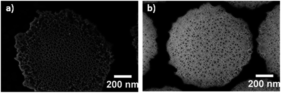 | ||
| Fig. 1 Top view SEM images of PSi pillars obtained from gold-patterned Si substrates after MACE treatment with two different etching solutions: (a) ethanol/HF/H2O2 and (b) water/HF/H2O2. | ||
In comparison, PSi obtained with EES has larger pores than PSi formed in WES. For electrochemical etching of Si it has already been reported that the addition of ethanol to the etching solution results in the formation of larger pores and a more homogenous porous silicon layer. These findings have been explained by the improved infiltration of the ethanol containing etching solution into the pores. In the case of water-based etching solutions the infiltration is hindered by the hydrophobic nature of silicon surface and by the attachment of formed bubbles.13 Similar results were reported in the context of fabricating biodegradable PSi barcode nanowires by Chiappini et al.14 In accordance with their findings, the presented experiments prove that the pore size of PSi can be modulated for the same wafer type by changing the composition of the etching solution. In general it is assumed that the following reactions occur during MACE.15
Cathode reaction (at the metal)
| H2O2 + 2H+ → 2H2O + 2h+ |
| 2H+ + 2e− → H2↑ |
Anode reaction
| Si + 4h+ + 4HF → SiF4 + 4H+, |
| SiF4 + 2HF → H2SiF6, |
Overall reaction
| Si + H2O2 + 6HF → 2H2O + H2SiF6 + H2↑ |
In this proposed reaction mechanism H2O2 reacts with the metal nanostructure and the formed holes (h+) are injected at the metal/Si interface into the Si valence band by diffusion.16 The hole injection due to H2O2 is too weak to result in significant etching by itself17 but the presence of the gold layer facilitates a stain etching mechanism leading to the formation of pores. However, this model is still under discussion and there is evidence that the holes cannot diffuse from the metal into the Si. Instead a polarization of the Si substrates is suggested which is based on the charging of the metal nanostructure after hole injection.18 Be that as it may, the formation of the presented PSi structures with dual pore sizes could be explained by the different availability of H+ and F− in the two employed etching solutions. Dissociation of HF in fluoride and hydrogen ions should be influenced by the presence or absence of ethanol in the etching solution. This hypothesis is supported by the faster reaction rate observed in WES in comparison to EES.
PSi sensors, composed of PSi pillars with large pores on top of a PSi layer with smaller pores, were prepared by consecutively etching gold patterned surface with both etching solutions (EES and WES). First, 3 mL of EES was dropped onto the substrate and after a certain amount of time the reaction was stopped by removing the etching solution. After rinsing the sample with ethanol and drying it in a stream of N2, the porous structure was immersed in 3 mL WES. This etching step was carried out for several s to min. It was also terminated by rinsing and drying. During the PSi fabrication two etching mechanism were observed leading first to the formation of a PSi monolayer and afterwards to the generation of PSi pillars. These observations could be traced back to the fine balance between two etching regimes: polishing (total dissolution of silicon) at the silicon surface in contact with the deposited Au and pore formation (partial dissolution of silicon) far from the metal. The rate of the reactions corresponding to the two regimes are influenced by several parameters such as the initial resistivity of the silicon substrate, the concentration of ethanol and the concentration of H2O2.14 Extensive experimental and theoretical work would be required in order to unravel the exact reaction mechanism. These experiments go far beyond the scope of this communication and are still under investigation.
Fig. 2a shows a SEM image of a PSi monolayer which was obtained after etching the gold patterned Si for 75 s with EES. Etching this sample afterwards in WES resulted in PSi structures whose appearance depended on the reaction time. If the sample was etched only for 90 s a PSi double layer was obtained (Fig. 2b). In the SEM image a distinct interface between the two porous layers is observed. Moreover, the PSi layers show different material contrast indicating that the porosities of the two layers are different. Pillar formation is limited and their height is less than 100 nm. A further increase in etching time resulted in a simultaneous increase in the length of the pillar structure and in the thickness of the bottom layer. After an etching time of 120 s the interface between the two differently porous layers almost coincide with the appearance of pillars (Fig. 2c). After a reaction time of 150 s different pore sizes within the pillars can be noticed (Fig. 2d). In Fig. 2e a SEM image of a porous Si structure is displayed which has been etched 10 s longer with respect to the sample presented in Fig. 2d. It can be easily noticed that once the pillars cross the interface of the two differently porous layers, the rate of pillar formation is increased. This can be attributed to the decrease in the resistivity of the second layer with respect to the first layer due to the relative difference in the pore diameter and hence in the thickness of the pore walls. Related results have been reported for electrochemical etching.13,19,20Fig. 2f shows a magnified view of the pillar interface.
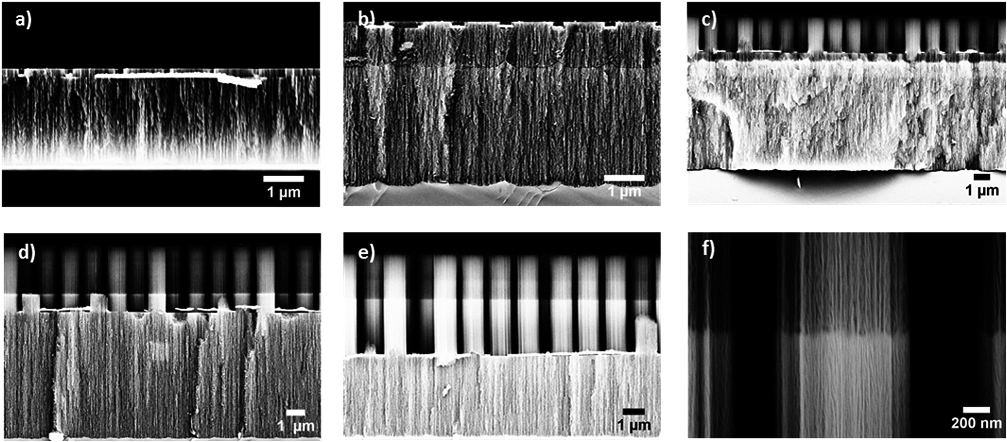 | ||
| Fig. 2 Cross sectional SEM images of the fabricated PSi structures. (a) PSi monolayer: EES, etched for 75 s; (b) PSi bilayer: EES 75 s, WES 90 s; (c) PSi-pillars bilayer: EES 75 s, WES 120 s; (d) PSi-pillar bilayer: EES 75 s, WES 150 s; (e) PSi-pillar bilayer: EEs 75 s, WES 160 s; (f) magnification of the pillar interface. | ||
Top view SEM images of the double layered PSi pillar structures revealed that the top of the pillars was blocked by an unidentified material (no more than 10 nm, Fig. S2†). This layer was observed in all samples fabricated by the double etching method.
In order to avoid the blocking of the pores, gold nanoparticles were deposited in the holes of the perforated gold film prior to MACE (Fig. S3†). Details of the procedure can be found in the ESI.† Fig. S4a and b† show SEM images of the resulting PSi structure with open pores which has been tested as optical sensor.
The reflectance spectrum is the base for PSi sensors utilizing changes in the interference pattern of the porous film for the detection of analytes. The fringe patterns are caused by interference of light rays which are reflected at the borders of the PSi film. Positions of fringe maxima can be predicted by the Fabry–Pérot relationship:
| mλm = 2nL |
The optical behavior of the fabricated PSi structures was studied with the help of RIFTS (Fig. 3). In Fig. 3a(i) a reflectance spectrum of a PSi pillar structure obtained by MACE with EES is displayed. The typical sinusoidal behavior, similar to an electrochemically etched PSi monolayer can be noticed. Representative reflectance spectra of double layer PSi pillar structures with and without gold film (shown in Fig. 2d, gold film removed with aqua regia) are depicted in Fig. 3a(ii) and (iii), respectively. The expected fringe pattern for a double layer with pillars is obtained. An enhancement of the reflectance signal was observed after the gold layer removal.
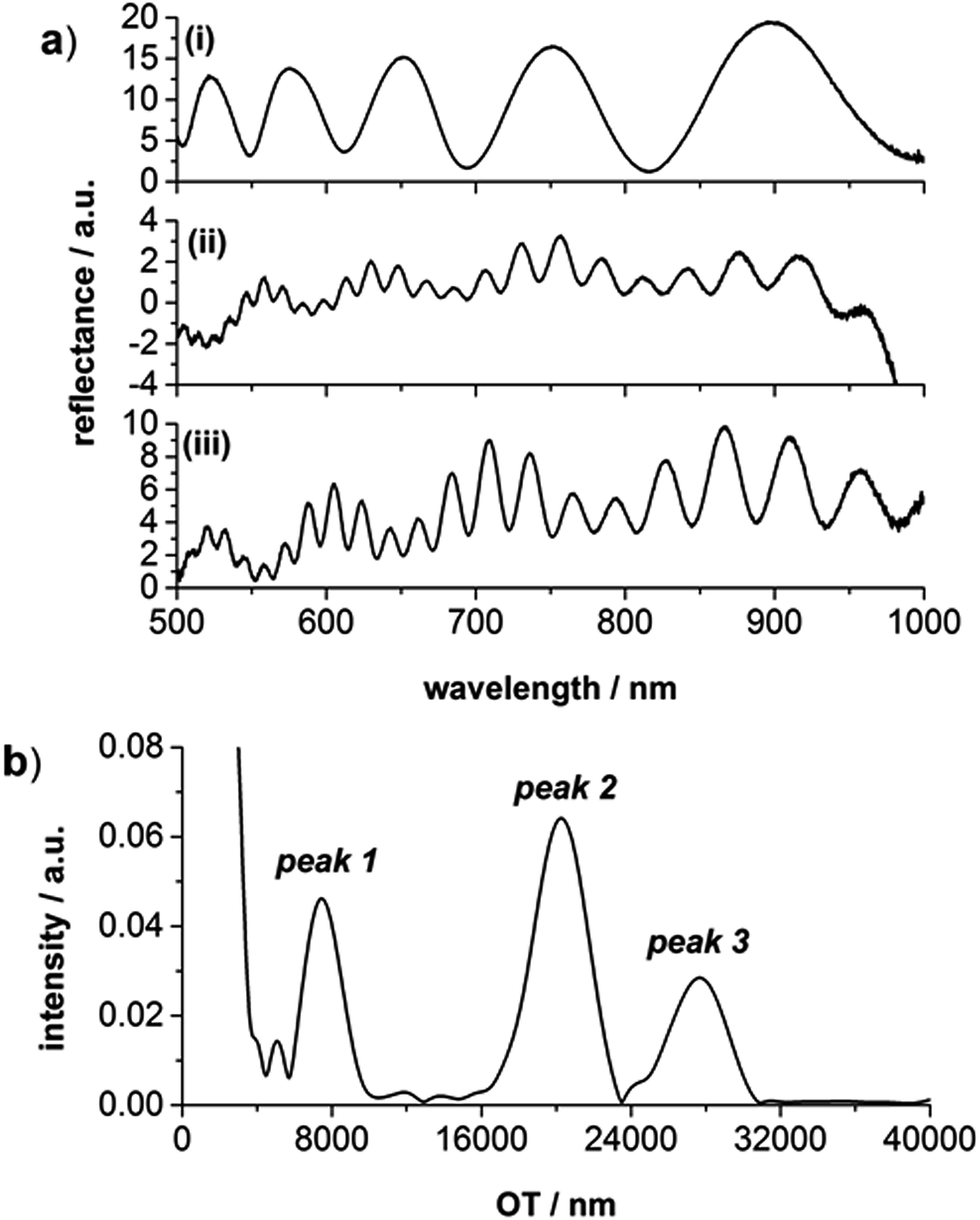 | ||
| Fig. 3 Optical characterization of the fabricated PSi structures. (a) After each production step a reflectance spectrum was recorded. Here, (i) is the spectrum of the structure obtained by etching with EES, (ii) spectrum of the structure after the second etch step with WES, (iii) spectrum of the PSi structure after gold removal. (b) The inverse spectrum of the reflectance spectrum of the PSi structure was analyzed using fast Fourier transform in order to obtain the characteristic OT peaks. | ||
Fig. 3b shows the FFT obtained from the inverse reflectance spectrum of the double layer PSi-pillar structure, which is characterized by three peaks at different OTs – in accordance with published results for PSi double layers fabricated electrochemically.23 Peak 1 corresponds to the layer with pillars, fabricated using EES, peak 2 can be assigned to the OT of the PSi layer prepared with WES, and peak 3 is related to the average OT of the two layers.
Finally, the presented PSi sensors, composed of a PSi bottom layer with small pores covered with hexagonally arranged PSi pillars with larger pores, were tested as a sensing platform for protein A and sucrose. By using two differently sized biomolecules (sucrose: 342.30 g mol−1, less than 2 × 2 × 2 nm; protein A: 42 kD, Stoke radius 5 nm) the special properties of the double layer sensor can be demonstrated which acts as molecular sieve. In the present case sucrose can enter both PSi layers whereas protein A is only admitted in the top layer with larger pores. For the sensing experiment the PSi sensor was first oxidized in air at 300 °C for 1 h in order to increase its stability against corrosion reactions.23 Afterwards, the sensor was placed in a flow cell and reflectance spectra were recorded in real time with a fiber optic spectrometer during the exposure of the sensor to different solutions. In general, three factors determine the magnitude of the optical response of the sensor to the presence of analytes: (1) changes in the refractive index of the buffer solution upon addition of analyte molecules, (2) size of the analyte molecules, and (3) the affinity of the analyte molecules to the sensor surface. In the presented sensing experiment, sucrose is detected by changes in the refractive index of the solution and protein A leads to changes in the reflectance spectrum due to adsorption to the sensor surface. Details of these experiments can be gleaned in literature.23,24 In Fig. 4 the shifts of the different peaks in the FFT of the inverse reflectance spectra are displayed which result from the penetration of sucrose or protein A into the pores. Fig. 4a shows changes in the position of peak 1 (Fig. 3b), corresponding to the porous pillars with large pores during the sensing experiment.
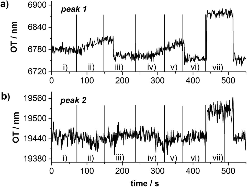 | ||
| Fig. 4 Optical response of the presented PSi sensor expressed as changes in the OT. Peak 1 corresponds to the OT of the pillar top layer and peak 2 is related to the OT of PSi bottom layer with smaller pores. The following solutions were consecutively flown over the sensor surface: (i) PBS pH 7.4, (ii) 0.25 mg mL−1 protein A in PBS, (iii) 0.1 M acetic acid followed by PBS pH 7.4, (iv) 0.25 mg mL−1 protein A in PBS, (v) 0.1 M acetic acid followed by PBS pH 7.4, (vi) 20% w/w sucrose in PBS, (vii) PBS pH 7.4. | ||
It can be clearly seen that both analytes, protein A and sucrose enter the porous pillars leading to an increase in the OT. Furthermore, the admission of protein A to the pores is relatively slow and its removal from the porous matrix surprisingly fast. These findings can be explained in two ways. On the one hand the sensor is rinsed with 0.1 M acetic acid solution in order to support the removal of protein A from the pores.24 On the other hand the top layer possesses strictly speaking two pore sizes: small pores in the pillars and the space between the pillars. The presented optical sensor cannot distinguish between these ‘pores’ and only detects the average refractive index of the PSi layer.
The position of peak 2 related to the bottom PSi layer with the smaller pores, does not shift during the exposure of the sensor to protein A solution, i.e. that protein A is too large for penetrating the porous layer (Fig. 4b). Only a smaller molecule like sucrose provoked an increase in the OT of this peak. These observations are in accordance with results obtained with electrochemically fabricated PSi double layer sensors suggesting the utilization of the presented PSi sensor as double beam interferometer (separate sensing and reference channel).
Conclusions
PSi sensors composed of hexagonally ordered PSi pillars with large pores on top of a PSi layer with smaller pores were fabricated by a combination of colloidal lithography, gold film deposition and MACE. By changing the composition of the etching solution in the MACE process differently sized pores were obtained. The resulting sensors show the expected sophisticated interference pattern in the reflectance spectrum. Its individual components are extracted from the spectrum by FFT enabling the detection of refractive index changes in the different porous ‘layers’ in real time. Thereby the penetration of differently sized biomolecules, namely protein A and sucrose, into the different PSi layers was successfully detected demonstrating the applicability of the presented PSi structure as optical sensor.Acknowledgements
VA acknowledges the financial support from CONACyT (# 188657). R. F. B. V. thanks CONACyT for the scholarship #329812. CP and R. F. B. V. are grateful for financial support from the Max Planck Society. CP acknowledges additional financial support from the BMBF (PhoNA, contract number: 03IS2101E).Notes and references
- Handbook of Porous Silicon, ed. L. Canham, Springer International Publishing, 2014 Search PubMed.
- C. Pacholski, Sensors, 2013, 13, 4694 CrossRef CAS PubMed.
- M. P. Stewart and J. M. Buriak, Adv. Mater., 2000, 12, 859–869 CrossRef CAS.
- H. Asoh, F. Arai and S. Ono, Electrochim. Acta, 2009, 54, 5142–5148 CrossRef CAS.
- L. Boarino, D. Imbraguglio, E. Enrico, N. De Leo, F. Celegato, P. Tiberto, N. Pugno and G. Amato, Phys. Status Solidi A, 2011, 208, 1412–1416 CrossRef CAS.
- S.-W. Chang, V. P. Chuang, S. T. Boles, C. A. Ross and C. V. Thompson, Adv. Funct. Mater., 2009, 19, 2495–2500 CrossRef CAS.
- X. Li, Curr. Opin. Solid State Mater. Sci., 2012, 16, 71–81 CrossRef CAS.
- K.-Q. Peng, X. Wang, L. Li, X.-L. Wu and S.-T. Lee, J. Am. Chem. Soc., 2010, 132, 6872–6873 CrossRef CAS PubMed.
- Z. Huang, N. Geyer, P. Werner, J. de Boor and U. Goesele, Adv. Mater., 2011, 23, 285–308 CrossRef CAS PubMed.
- X. Liu, P. R. Coxon, M. Peters, B. Hoex, J. M. Cole and D. J. Fray, Energy Environ. Sci., 2014, 7, 3223–3263 CAS.
- M. Sainato, L. M. Strambini, S. Rella, E. Mazzotta and G. Barillaro, ACS Appl. Mater. Interfaces, 2015, 7, 7136–7145 CAS.
- C. Pacholski, Phys. Status Solidi C, 2011, 8, 1797–1800 CrossRef CAS.
- O. Bisi, S. Ossicini and L. Pavesi, Surf. Sci. Rep., 2000, 38, 1–126 CrossRef CAS.
- C. Chiappini, X. Liu, J. R. Fakhoury and M. Ferrari, Adv. Funct. Mater., 2010, 20, 2231–2239 CrossRef CAS PubMed.
- X. Li and P. W. Bohn, Appl. Phys. Lett., 2000, 77, 2572–2574 CrossRef CAS.
- K. W. Kolasinski, Curr. Opin. Solid State Mater. Sci., 2005, 9, 73–83 CrossRef CAS.
- C. M. A. Ashruf, P. J. French, P. Bressers and J. J. Kelly, Sens. Actuators, A, 1999, 74, 118–122 CrossRef CAS.
- K. Kolasinski, Nanoscale Res. Lett., 2014, 9, 1–8 CrossRef CAS PubMed.
- V. Lehmann, F. Hofmann, F. Möller and U. Grüning, Thin Solid Films, 1995, 255, 20–22 CrossRef CAS.
- G. Gesele, J. Linsmeier, V. Drach, J. Fricke and R. Arens-Fischer, J. Phys. D: Appl. Phys., 1997, 30, 2911 CrossRef CAS.
- V. S. Y. Lin, K. Motesharei, K.-P. S. Dancil, M. J. Sailor and M. R. Ghadiri, Science, 1997, 278, 840–843 CrossRef CAS PubMed.
- C. Pacholski, L. A. Perelman, M. S. VanNieuwenhze and M. J. Sailor, Phys. Status Solidi A, 2009, 206, 1318–1321 CrossRef CAS.
- C. Pacholski, M. Sartor, M. J. Sailor, F. Cunin and G. M. Miskelly, J. Am. Chem. Soc., 2005, 127, 11636–11645 CrossRef CAS PubMed.
- C. Pacholski, C. Yu, G. M. Miskelly, D. Godin and M. J. Sailor, J. Am. Chem. Soc., 2006, 128, 4250–4252 CrossRef CAS PubMed.
Footnotes |
| † Electronic supplementary information (ESI) available: Materials and methods, experimental details, additional SEM images. See DOI: 10.1039/c5ra26816h |
| ‡ Present address: University of Potsdam, Institute of Chemistry, Am Mühlenberg 3, 14476 Potsdam, Germany, E-mail: cpachols@uni-potsdam.de. |
| This journal is © The Royal Society of Chemistry 2016 |