
The hierarchical porosity of a three-dimensional graphene electrode for binder-free and high performance supercapacitors†
Jun-He Changab,
Yu-Han Hungab,
Xu-Feng Luod,
Chi-Hsien Huangc,
Sungmi Junge,
Jeng-Kuei Changd,
Jing Konge and
Ching-Yuan Su*ab
aGraduate Institute of Energy Engineering, National Central University, Tao-Yuan 32001, Taiwan. E-mail: cysu@ncu.edu.tw
bDepartment of Mechanical Engineering, National Central University, Tao-Yuan 32001, Taiwan
cDepartment of Materials Engineering, Ming Chi University of Technology, New Taipei City 24301, Taiwan
dGraduate Institute of Material Science and Engineering, National Central University, Tao-Yuan 32001, Taiwan
eDepartment of Electrical Engineering and Computer Sciences, Massachusetts Institute of Technology, 77 Massachusetts Avenue, Cambridge, MA 02139, USA
First published on 14th January 2016
Abstract
In this study, we report a binder-free supercapacitor including a unique graphene electrode of hierarchical porosity composed of the submicrometer porosity (∼20 μm) of 3D graphene self-assembled by nanopores (∼2.5 nm) of graphene flakes. The hierarchical 3D porosity of the graphene electrode was prepared by a facile and scalable approach based on acid activation and freeze-drying. Remarkably, we found that this unique graphene-based electrode, when used in a supercapacitor, shows improved performance compared with a reported graphene electrode; these improvements include high specific capacitance (∼442 F g−1), fast rate charging/discharging, and excellent cycle stability (95% after 1600 cycle numbers), which were due to (1) the creation of a high specific surface area and a diffusion path, thus promoting ion transport capability, and (2) the additional pseudocapacitor due to the controlled oxygen amount of functionalization on the graphene surface. The resultant device shows an energy density of 51.9 W h kg−1 and a power density of 467.8 W kg−1. This study introduces a new concept for the binder-free, cost-effective and high performance of a graphene-based supercapacitor, which could pave the way for practical applications in frontier energy devices.
Introduction
Graphene-based electrical energy storage devices, such as Li-ion batteries (LIBs) and supercapacitors, have attracted intensive attention in recent years due to their unique characteristics of high specific capacitance, long cycling stability and excellent mechanical flexibility.1–5 In particular, supercapacitors show rapid charge/discharge storage mechanisms and a higher power density than LIBs, enabling supercapacitors to be potential applied in portable electronics and hybrid electric vehicles. Currently, supercapacitor technology is subdivided into two classes: electrochemical double-layer capacitors (EDLCs) and pseudocapacitors.6,7 The EDLCs are based on reversible ion adsorption on the interface of the electrode and electrolyte when subjected to a voltage bias.8 Therefore, for the supercapacitor, the formation of an available high surface area on the electrode can significantly increase the amount of charge storage per unit mass (F g−1). The recent works using graphene as the EDLC electrode material were mainly due to its excellent electrical conductivity, ultrahigh specific surface area (SSA) and chemical stability.7,9–11 The theoretical SSA in graphene is 2675 m2 g−1, and the capacitance is estimated to be 550 F g−1.6,7 To achieve the requirements of energy devices, it has been reported that the efficient ionic and electron transport kinetics are key for the high density and high performance of a supercapacitor.12 However, recent works involving reduced graphene oxide (rGO-derived) or graphene flakes as electrodes show lower ion diffusion due to the parallel restacking of two-dimensional graphene sheets when they were assembled into electrodes; thus, the restacking significantly degrades the specific surface area.13,14 Recent reports demonstrate the construction of macroscopic three-dimensional (3D) bulk assemblies of graphene with an enhanced high SSA for versatile applications. These 3D frameworks can be produced via chemical vapor deposition (CVD) over catalytic metal foam or via self-gelation from the bottom-up assembly of GO or graphene flakes.15–21 The porosity is over the microscale range of ∼20 μm to 70 μm. Recent reports show that the graphene-based monoliths exhibit ultralow density, high elasticity and electrical conductivity and thus show potential especially for the hybrid electrode in energy storage applications.22 To date, numerous reports have studied hybrid electrodes for use in energy storage by constructing 3D porous frameworks for increasing the SSA and ion and electron transport.15,23–26 Tao et al., reported the ultrahigh volumetric capacitance of up to 376 F cm−3 by altering porous structured graphene as an electrode in an aqueous electrolyte (KOH). More importantly, the assembly of a porous graphene electrode in a supercapacitor led to a binder-free electrode without any additives, resulting in a high energy density storage device that can be used in practice.27 Zhu et al. reported the first work on the electrochemical capacitance of 3D graphene with an ionic liquid electrolyte (EMIMBF4/AN), resulting in a high energy density of ∼68 W h kg−1.28 Zhang et al. demonstrated the unique performance of high ion and electron transportation of graphene hydrogels for supercapacitors with high rate capability, where the reduced graphene electrode exhibited a high specific capacitance of 220 F g−1 at 1 A g−1, and it maintained 74% of the capacitance for high rate discharging up to 100 A g−1, thus making it promising for high rate charge/discharge devices.29 As for the solid-state supercapacitors, Xu et al. reported the fabrication of a flexible solid-state supercapacitor based on a 3D macroporous graphene electrode by utilizing H2SO4–polyvinyl alcohol (PVA) as a gel electrolyte, exhibiting a gravimetric specific capacitance of 196 F g−1. Moreover, the excellent cycling stability and mechanical flexibility highlight the potential of such a supercapacitor for use as a high performance flexible energy storage device. In addition, Zhu et al. reported that the 3D graphene structure decorated with metal oxide as a hybrid electrode (3D graphene/CoO nanorod) is able to take advantage of both EDLCs and pseudocapacitors for energy storage, where the 3D graphene was employed as a conductive supporting electrode with a large number of host sites for the pseudocapacitive active material of cobalt oxide.30 The hybrid electrode achieved an extremely high capacitance of ∼600 F g−1 at 20 A g−1.Compared with the 3D macroporous graphene structure, an alternative approach to increase the SSA of a graphene electrode is to create nanopores on the graphene basal plane. Such a mesoporous holey graphene structure can be prepared in a facile manner by the traditional activation procedure. The well-known approach is KOH activation for carbon materials, including activated carbons and carbon nanotubes or fibers as well as graphene nanosheets.31 Such activated carbon materials have been regarded as potential materials for electrochemical energy systems.32 In 2011, Zhu et al. employed KOH activation of exfoliated graphene sheets to create nanopores (primarily 0.6–5 nanometer pores) on sp2 carbon networks, resulting in a superior high SSA of up to 3200 m2 g−1.11 The constructed electrode in a supercapacitor yielded a high gravimetric capacitance of 166 F g−1 in the electrolyte of 1-butyl-3-methylimidazoliumtetrafluoroborate (BMIM BF4/AN) at a constant current of 5.7 A g−1 and a working voltage of 3.5 V. The energy density and power density were 70 W h kg−1 and 250 kW kg−1, respectively. In 2013, Zhang et al. demonstrated a hydrothermal carbonization process on a GO and sucrose mixture, followed by KOH activation. The as-prepared graphene porous materials with pore size distributed from 0.5–5 nm exhibited an ultrahigh SSA of 3523 m2 g−1. The resultant specific capacitance and energy density based on this electrode were 231 F g−1 and 98 W h kg−1, respectively.33 Zhao et al. reported another activation process to obtain a cleaner nanoporous graphene product, by using HNO3 as reactive agents, comprising sonication to generate in-plane porosity on graphene sheets, followed by thermal reduction to complete the process;34 the LIBs made by these materials show excellent high-rate Li-ion storage capabilities due to the enhanced ion diffusion kinetics.
The aforementioned concept with the 3D graphene macroporous structure and the 2D holey graphene structure can both significantly increase the SSA on the bulk scale, resulting in the excellent energy storage performance of the graphene-based supercapacitor. However, there is still a lack of reports on combining both of these two structures as an electrode for use in energy storage. This knowledge gap motivated this work, where the microporous 3D graphene scaffold provides an interconnected conductive electrode for ion permeation, while the assembly of nanoporous holey graphene creates another set of ion diffusion paths for propagation through these 3D graphene electrodes.
Here, we fabricate and characterize a binder-free graphene-based supercapacitor integrated with 3D self-assembled nanoporous graphene as a hybrid electrode by facile approaches of activation and freeze-drying. The as-prepared functionalized electrode exhibit a SSA of up to 564 m2 g−1. The optimized condition allows us to yield an average capacitances of 364 F g−1 and highest specific capacitances of ∼442 F g−1 at a rate of 2 A g−1. The energy density and power density are 51.9 W h kg−1 and 467.8 W kg−1, respectively. Moreover, the superior cycling stability and rate capabilities suggest the high ion permeance and high electronic conductivity of this unique and multifunctional graphene electrode. The reported approach is facile, scalable and cost-effective, which is promising for the production of high performance graphene-based energy storage devices.
Results and discussion
In this work, the starting material was graphene oxide (GO), which was prepared by the improved Hummers' methods (see the experimental section for details). Fig. 1 shows the morphology of as-prepared GO flakes. Fig. 1a and b show the typical AFM image and the height profile, revealing flakes with sizes of up to 45 μm and a typical thickness of 1.02 nm. Fig. 1c and d show SEM and TEM images, which display the clean surface and the wrinkled structure on the basal plane of a graphene flake, implying that high-purity thin-layered flakes were obtained. To construct the 3D bulk electrode self-assembled nanoporous graphene, the process comprises three steps, as illustrated in Fig. 2a: (1) creation of nanopores on GO through an activation process; (2) self-assembly of the 3D graphene monolith by freeze-drying; and (3) thermal reduction of 3D graphene. Fig. 2b shows the photo images for the as-prepared GO 3D monolith and the corresponding reduced graphene electrode, where the monolithic size can be adjusted by tailoring the initial mode. The reduced graphene monolith shows mechanical elasticity and compressibility (see the ESI movie clip†), which is beneficial for a durable electrode in an energy storage device. Fig. 2c shows SEM images for the microstructure of a 3D graphene monolith, exhibiting the interconnected graphene with the porous network. The pore size ranged from a few micrometers to tens of micrometers, and the average value was approximately 20 μm, as revealed in the magnified image. Moreover, to create the nanopores on the graphene flakes (i.e., holey graphene), the activation process is carried out according to a facile method using a mixture of GO solution with 70% concentrated HNO3 under water-based sonication.35,36 During the process, the induced high strain from the cavitation bubbles by the acoustic pressure creates a scission force on the graphene basal plane and then breaks the carbon framework. Next, the HNO3 reacts with these defect sites on the edges, resulting in the removal of carbon atoms from the GO flakes. Fig. 2d and e show typical TEM images for the pristine GO and the activated GO sheets. The image for the GO after the activation treatment reveal large amounts of highly dense nanopores over the entire basal plane of the GO flake (Fig. 2e), in clear contrast to the control sample of pristine GO flakes (Fig. 2d). To verify the mesoporous structure of the active graphene, N2 adsorption–desorption analysis was performed. Fig. 2f shows the highest pore volume with the pore size ranging from 2.0–4.5 nm, primarily at ∼2.14 nm. The pore size distribution was consistent with the statistically estimated nanopore size distribution from the high magnified HRTEM observation (see Fig. S1†). The results imply the efficient formation of holey graphene by such an acid treatment. It has been reported that the degree of reduction conditions significantly affect the surface chemical and physical properties, such as electrolyte wetting, charge transferring and electrical conductivity, due to the complex composition of oxidized functional groups, resulting in different electrochemical performance.37,38 In addition, the proposed nanoporous graphene during the activation procedure and the 3D structure might affect these properties. To study in detail the effects of the 3D structure and surface chemistry properties on the electrochemical performances, several samples were prepared with various conditions, including different annealing temperatures (arranged from 400–800 °C) and different structured graphene (see excremental section for the sample definitions and detail conditions).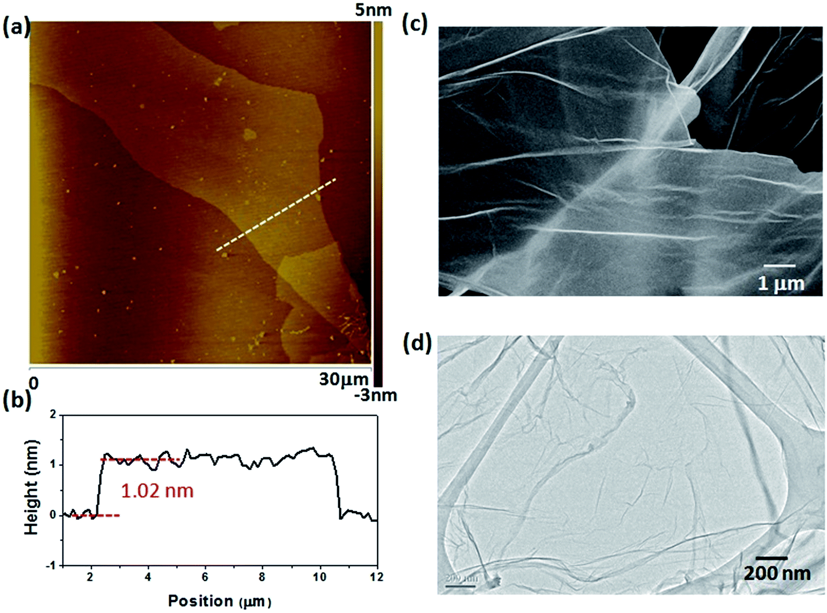 | ||
| Fig. 1 (a) Typical AFM images of the GO sheet. (b) The corresponding height profile for the graphene sheet in (a), indicating that the sheet is approximately 1.76 nm in thickness. (c) SEM image of the surface morphology of the graphene sheets. (d) TEM image of a graphene sheet, showing the wrinkles over the surface of the sheet. | ||
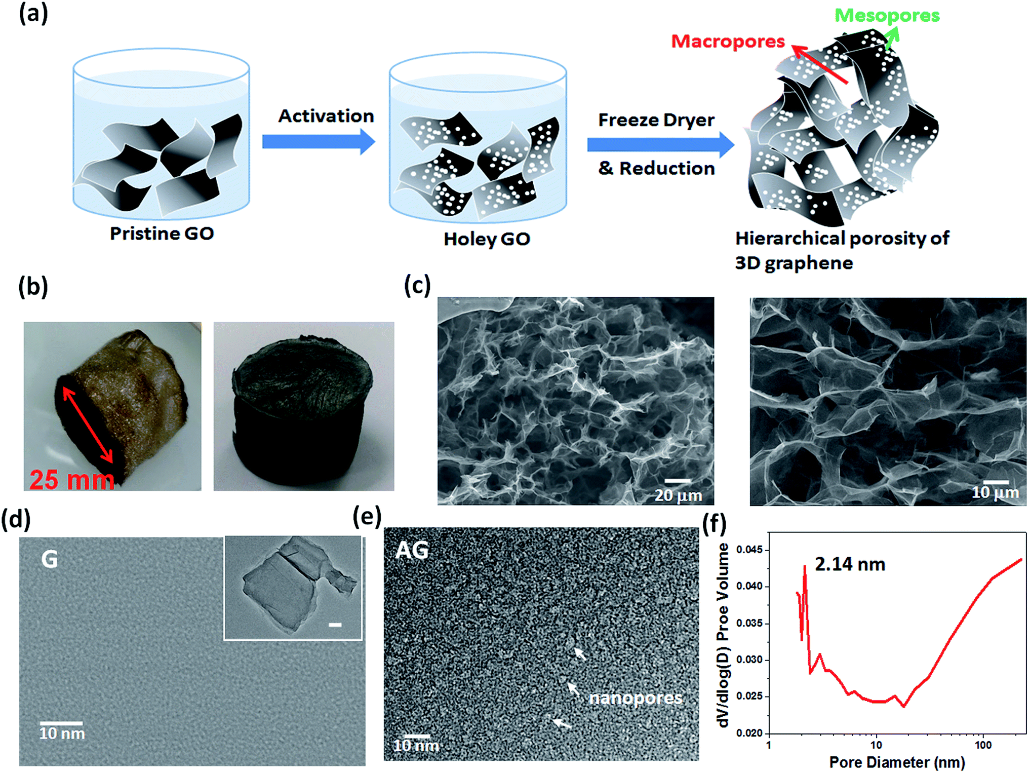 | ||
| Fig. 2 (a) The schematic illustration of the procedures to construct 3D monolithic self-assembled nanoporous graphene. (b) The photo images for the as-prepared 3D graphene foam via freeze-drying (left) and after thermal reduction (right). (c) The low- and high-magnification SEM images of the 3D graphene in (b). (d) The HRTEM image of pristine GO; the inset shows a low magnification image (scale bar is 100 nm). (e) The nanoporous graphene after acid activation, where the white arrows indicate the nanopores on the sheet surface. (f) The pore size distribution of nanoporous graphene after activation, which was characterized by the N2 adsorption–desorption isotherms analysis. | ||
Fig. 3a shows the XPS C 1s spectra and the corresponding deconvoluted peaks on samples produced via thermal reduction or samples produced by the combination of activation and thermal reduction at various temperatures. The oxidized functional groups on the in-plane graphene were mainly C–O, C![[double bond, length as m-dash]](https://www.rsc.org/images/entities/char_e001.gif) O, and O–CO, centered at 286.7, 287.8, and 288.9 eV, respectively. The integrated areas of deconvoluted peaks from C 1s bonding states are plotted in Fig. 3b, and the values are listed in Table 1. The C/O ratio clearly increased with increased reduction temperature due to the effective removal of oxidized groups, especially the reduction of C–O bonds. Moreover, the C/O ratio clearly decreased and the CO and O–CO components became more prominent when the GO was subjected to the activation procedures. In addition, the C–O shows lower intensity for the nanoporous graphene after the activation treatment. This result indicates the enrichment of CO and O–CO groups on the as-prepared holey graphene. This result is also consistent with the activated carbon materials in reported works.34 The same features can also been distinguished from the phonon mode of the Raman spectra, as shown in Fig. 3c, where the integrated area intensity ratio of the D peak to G peak (I(D)/I(G)) is slightly increased when the sample was treated with HNO3 activation. The results suggest a higher defect degree arising from large amounts of edge states on the basal plane of holey graphene flakes (Table 2).
O, and O–CO, centered at 286.7, 287.8, and 288.9 eV, respectively. The integrated areas of deconvoluted peaks from C 1s bonding states are plotted in Fig. 3b, and the values are listed in Table 1. The C/O ratio clearly increased with increased reduction temperature due to the effective removal of oxidized groups, especially the reduction of C–O bonds. Moreover, the C/O ratio clearly decreased and the CO and O–CO components became more prominent when the GO was subjected to the activation procedures. In addition, the C–O shows lower intensity for the nanoporous graphene after the activation treatment. This result indicates the enrichment of CO and O–CO groups on the as-prepared holey graphene. This result is also consistent with the activated carbon materials in reported works.34 The same features can also been distinguished from the phonon mode of the Raman spectra, as shown in Fig. 3c, where the integrated area intensity ratio of the D peak to G peak (I(D)/I(G)) is slightly increased when the sample was treated with HNO3 activation. The results suggest a higher defect degree arising from large amounts of edge states on the basal plane of holey graphene flakes (Table 2).
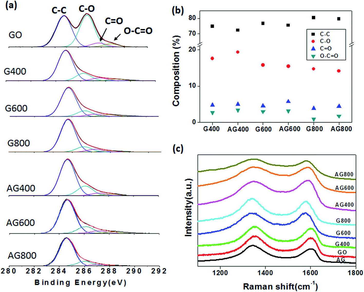 | ||
| Fig. 3 (a) The deconvoluted C 1s XPS spectra of GO, thermally reduced GO (G 400 –G 800), and activated GO followed by thermal reduction (AG 400–AG 800). (b) The compositions of C bonding states, including C–C, C–O, CO, and O–CO, in various samples, obtained by the integrated peak areas from the C 1s spectra in (a). (c) The corresponding Raman spectra of GO, G and AG samples. | ||
| Sample | C/O ratio | C 1s XPS peak area ratio (%) | Raman | |||
|---|---|---|---|---|---|---|
| C–C | C–O | CO |
O–CO |
ID/IG | ||
| G 400 | 7.5 | 74.89 | 17.57 | 4.81 | 2.73 | 1.39 |
| AG 400 | 3.9 | 72.23 | 19.33 | 5.03 | 3.41 | 1.34 |
| G 600 | 8.1 | 76.63 | 15.80 | 4.55 | 3.02 | 1.39 |
| AG 600 | 6.5 | 75.54 | 15.47 | 5.76 | 3.24 | 1.43 |
| G 800 | 15.7 | 80.52 | 14.70 | 3.84 | 0.95 | 1.48 |
| AG 800 | 14.8 | 79.65 | 14.14 | 4.42 | 1.80 | 1.59 |
| Sample | Before absorption (mg) | After (mg) | Uptake (mg) | Estimated SSA (m2 g−1) |
|---|---|---|---|---|
| FAG 400 | 2.6 | 3.3 | 0.7 | 564 |
| FG 400 | 3.5 | 4.2 | 0.7 | 508 |
| AG 400 | 1.7 | 2 | 0.3 | 448 |
| G 400 | 2 | 2.3 | 0.3 | 381 |
To investigate the influence of different graphene structures on the electrochemical performance, the three-electrode testing system with the electrolyte of KOH aqueous solution was used (see Fig. S2† for details on the setup). The testing electrodes composed of graphene materials were prepared by supporting graphene in a Ni foam, followed by the direct thermal drying or freeze-drying procedures; the photo images and SEM images are shown in Fig. S3.† The results show that the graphene flakes spontaneously crumpled and restacked over the surface of the Ni ligaments following the direct thermal drying process, while the 3D porosity graphene could be retained among the Ni foam without restacking following the freeze-drying process. Herein, the Ni foam supporting the electrode was found to load graphene uniformly; however, Ni might be expected to participate in the electrochemical reaction during the measurements. Nevertheless, the cyclic voltammetry (CV) curves in Fig. S4† revealed a negligible capacitance contribution from the pristine Ni foam compared with the graphene samples, indicating that it is appropriate to hybridize graphene with the Ni foam as a binder-free electrode. Moreover, there were no apparent phenomena of the peel-off of graphene from the electrode when the electrode was subjected to a 2000-cycle test, suggesting the mechanical strength and operational reliability of the as-prepared graphene hybrid electrode ((c) in Fig. S2†). Fig. 4a shows the compiled CV curves for different structured graphene samples under thermal reduction at 400 °C, where all the CV curves exhibit a quasi-rectangular shape (other CV curves with different temperatures are also shown in Fig. S5†), indicating a nearly ideal supercapacitive characteristic. Compared with all the curves, the 3D self-assembly of graphene (FG 400) shows higher capacitance than that of restacked holey graphene (AG 400), suggesting that the macroporous structure dominates the ion propagation more efficiently than the nanoporous structure. Moreover, the 3D self-assembly of holey graphene (FAG 400) shows superior high performance than other conditions, suggesting that the hierarchical porosity of the 3D monolith assembled from holey graphene, especially its macroporous structure, dominates and enhances the capacitive performance. Note that the curve from FAG 400 shows apparent redox peaks, indicating the additional contributions of pseudocapacitance beside the EDLC, which is mainly attributed to the larger amount of oxygen groups on graphene at a lower reduction temperature (see the C/O ratio in Table 1). In addition, FAG 400 shows more clear redox peaks than AG 400, revealing the existence of many oxygen-functional groups exposed to react with the ion electrolyte due to the increase of the more accessible surface area created in the macroporous structure.
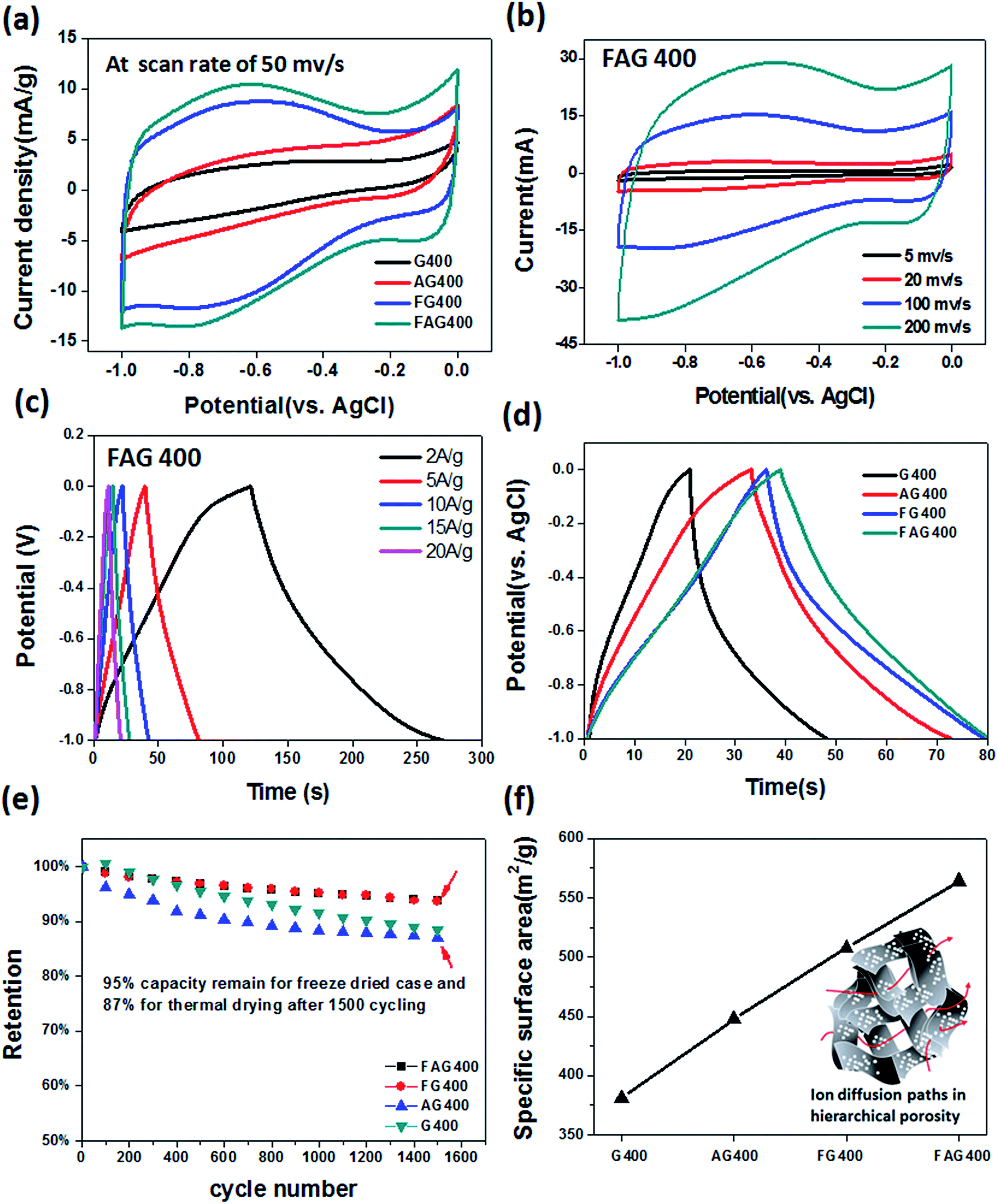 | ||
| Fig. 4 The electrochemical performances of various structured graphene supercapacitors in 6 M KOH aqueous solution. (a) The compiled CV curves at a scan rate of 50 mV s−1 for various structured graphene samples. (b) The typical CV curve for sample FAG 400 at various scan rates. (c) The corresponding GCD curves of FAG 400 performed at different current densities. (d) The comparison of GCD curves at current density of 5 A g−1 for FG 400 and FAG 400. The raising and decline branch represent the charge and discharge steps, respectively. (e) Cycling stability tests for various structured graphene samples at a scan rate of 200 mV s−1. (f) The plots reveal the SSA on various graphene electrodes. The inset shows an illustration indicating the creation of many ion permeation paths for the 3D structure self-assembled holey graphene (FAG 400). | ||
In this work, the FAG sample always shows higher performance than the other samples. Taking FAG 400 as an example, Fig. 4b shows typical CV curves for FAG 400 at various scan rates; the current response increases accordingly with an increase in scan rate from 5 mV s−1 to 200 mV s−1, and the CV curves maintain their rectangular shape without severe distortions, implying the excellent rate performance and low internal resistance. Fig. 4c shows the galvanostatic charge–discharge (GCD) curves for FAG 400 at different current densities, where the nearly symmetric triangle curves were observed for the current densities ranging from 2 A g−1 to 20 A g−1, consistent with EDLC features. The specific capacitance is calculated to be 442 F g−1 at 2 A g−1, which is superior to that for the other conditions shown here and is comparable to the best performance of graphene-based supercapacitors. Moreover, from the GCD curve (Fig. 4d), FAG 400 shows a smaller voltage IR drop (1.6 mV) than FG 400 (3.4 mV), AG 400 (11.1 mV) and G 400 (34.1 mV), indicating the lower equivalent series resistance (ESR) for FAG 400. Furthermore, Fig. 4e shows the tests for the cycling stability; FAG 400 could retain 95% of the initial capacitance over 1600 cycles, indicating excellent cycling stability at a high current scan rate of 200 mV s−1. The above discussions demonstrate that the tailored graphene electrodes made from various structures highly affect the supercapacitor performances, suggesting that the high accessible surface area in FAG samples promotes the ion diffusion dynamic along both the macropores and the nanopores of the graphene electrode. To verify this suggestion, the specific surface area (SSA) values were estimated on different structured graphene electrodes by methylene blue (MB) dye adsorption methods (see the Experimental section). Fig. 4f reveals that the FAG samples shows SSA of ∼564 m2 g−1, which is ∼48% higher than that of the restacking graphene electrode (G 400 ∼ 381 m2 g−1), indicating that the combination of the macroporous structure of the 3D monolith and the nanopores on the holey graphene sheets could highly increase the SSA and thus create many ion permeation and diffusion paths (as illustrated in the inset of Fig. 4f and additional N2 adsorption–desorption isotherms characterization can be referred to Fig. S10†).
In addition to the effect of the micro/nanostructures, the samples at different reduction temperatures also reveal variations in their electrochemical properties. Fig. 5a shows the compiled CV curves for the FAG samples with different thermal reduction temperatures of 400, 600, and 800 °C. Note that the samples with higher temperature treatment show a decayed capacitance over all structure conditions (i.e., G, AG, FG, and FAG samples), which could be attributed to two main reasons: (1) the decrease of the interlayer spacing and (2) the loss of oxidized-functional groups. Previous reports have shown that the interlayer spacing of stacking graphene gradually decreased from 3.78 Å to 3.37 Å when it was reduced at temperatures from 200 to 900 °C due to the removal of oxygen-containing functional groups between the graphene interlayer.39 The decrease of the interlayer spacing lowers the accessible passage for ions diffusing to the interior graphene surface and thus degrades its charging/discharging process. The second reason for the decayed capacitance at higher temperature is the loss of most oxidized functional groups on the graphene surface, as shown in Fig. 3a, because these functional groups were regarded as facilitating the redox process on the graphene surface, which could provide the additional effect of pseudocapacitance.40 However, the existence of functional groups on graphene also helps to enhance the wettability, and this wettability could highly improve the ionic accessibility between the electrolyte and electrode.26,41 Fig. S6† shows that the contact angle increases from 73° to 88° with increasing reduction temperature from 400 to 800 °C, indicating the higher wettability of graphene with the electrolyte at lower temperature reduction. Therefore, the partial removal of oxidized functional groups from the graphene surface by moderate reduction of GO results in suitable surface chemistry properties for obtaining higher ionic propagation capability. To study the details of the optimized conditions for the graphene electrodes, the additional conditions of thermal reduction at 300 °C (FAG 300) and 500 °C (FAG 500) were studied (see Fig. S7†). When the temperature is lower than 400 °C (FAG 300), the electric conductivity was apparently degraded, resulting in a lower capacitance of 197 F g−1 due to the higher internal series resistance. Herein, the voltage IR drops were probed to study the series resistance, as shown in Fig. 5b, where FAG 400 reveals an unexpected smaller IR drop (7.1 mV) than that of FAG 600 (49.8 mV) and FAG 800 (89.1 mV), suggesting the lower equivalent series resistance for 400 °C reduction. To further understand the rate performance and the ion diffusion kinetics of the FAG samples, electrochemical impedance spectroscopy (EIS) was used in this study. Fig. 5c shows the Nyquist plot taken from 106 Hz to 0.1 Hz. In the low frequency regime, the nearly vertical line indicates the pure capacitive behaviors of FAG 400. In the high frequency regime (the inset in Fig. 5c), the Nyquist plot reveals a smaller diameter of the semicircle for FAG 400 than for the others, confirming the lower charge transfer resistance and highly efficient ion diffusion within such hierarchical porosity structures of the FAG samples. In addition, the nearly 45° angle in the Warburg region is a typical characteristic for an electrolyte permeated and saturated within a porous electrode.42 Moreover, the x-intercept of the Nyquist plot has been reported to probe the equivalent series resistance (ESR) of the electrode. In this work, FAG 400 shows a smaller x-intercept value of ∼0.59 Ω than FAG 600 (0.71 Ω) and FAG 800 (0.86 Ω), implying the relatively small ESR, which is attributed to the shortened ion diffusion paths in the unique hierarchical porosity of the FAG structure, as shown in the inset of Fig. 4f. Fig. 5d shows the rate capacitances for the FAG samples, including for FAG 400, where the electrode exhibited the specific capacitance of 247 F g−1 and 188 F g−1 as the current density increased from 2 to 20 A g−1 (maintaining 76% of the specific capacitance), indicating the high rate properties. Note that the lower capacitance shown here compared with the capacitance obtained from the CV curve (Fig. 5e) is mainly due to the different scan rate (see Fig. S8† for details). The high rate performance is enabled by the fast charge transfer of the high conductivity graphene electrode, resulting in an excellent discharge process at high current density.43
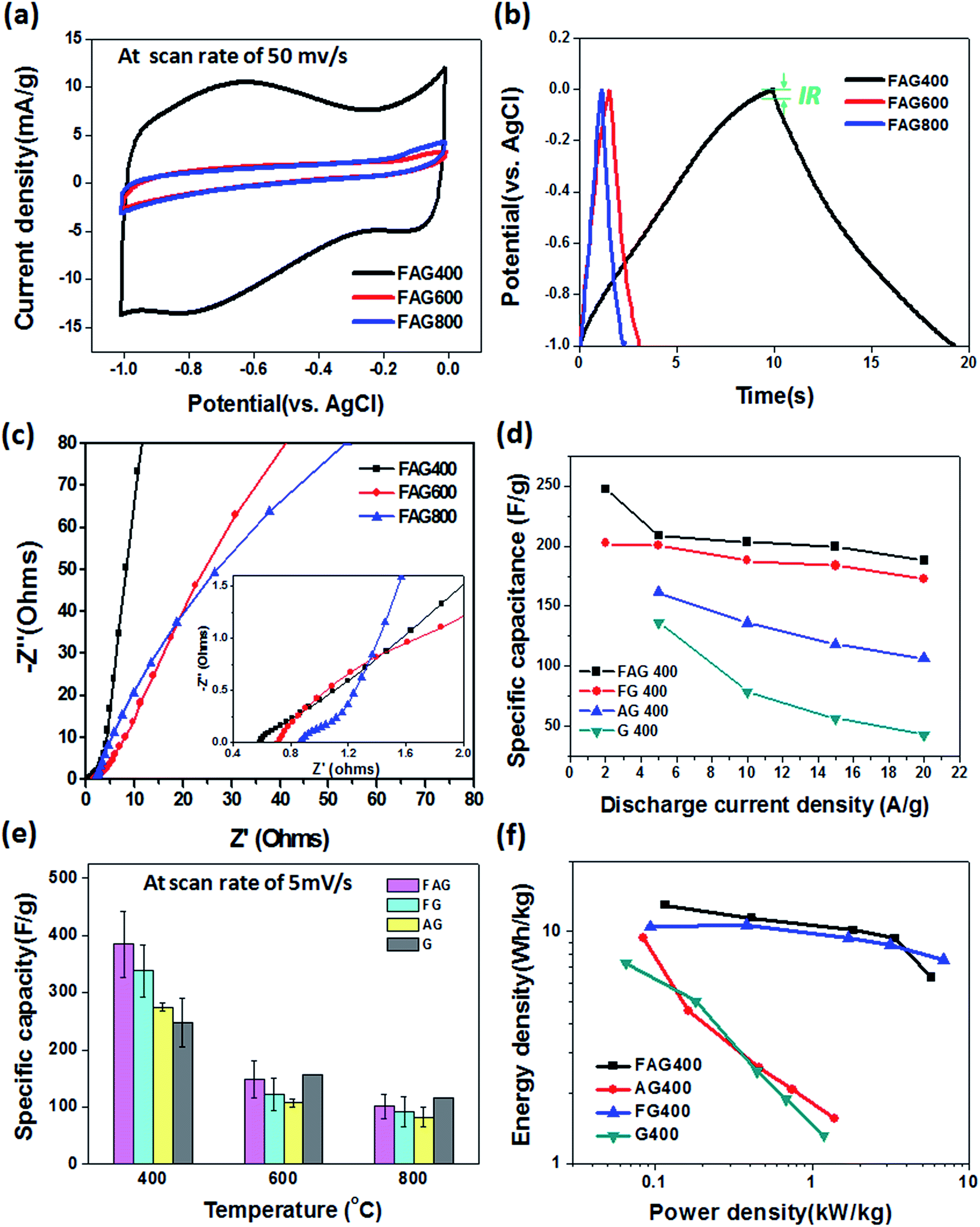 | ||
| Fig. 5 The electrochemical performances of the graphene electrode under various degrees of oxidized functionalization. (a) The CV curves for the FAG sample under different reduction temperatures and (b) the corresponding GCD curves measured at current density of 20 A g−1. The IR drop is derived from the discharge branch. (c) The Nyquist plot for the FAG samples (inset shows the high-frequency region). (d) The rate capacitances of the FAG samples at various current densities. (e) The compiled statistical analysis on the specific capacitance for all the graphene-based electrodes studied here. (f) The Ragone plot of the power density versus the energy density for symmetric supercapacitors with different graphene electrodes. | ||
Fig. 5e plots the histograms for the compiled specific capacitance for all the studied graphene-based electrodes. The result clearly shows that FAG 400 allows for obtaining the average capacitance of 384 F g−1 (corresponding to an areal capacitance of 0.66 F m−2), with the highest capacitance being up to ∼442 F g−1. This value is also superior to most of those in the reported works on graphene-based supercapacitors (as listed in Table S1†). From the view point of the electrode structure, the hierarchical porosity of the FAG samples comprises macropores and nanopores in the graphene monolith, which provide the most efficient ion diffusion process. However, the moderate thermal reduction temperature results in the excellent surface chemistry and electrical conductivity of the graphene electrode. The partial removal of the oxygen-functional groups on the graphene surface not only retains the larger interlayer spacing (i.e., high SSA), which is beneficial for ion transport, but also provides the additional pseudocapacitance properties in addition to the EDLC. Thus, the capacitance comprising these factors significantly promotes the capacitance performances. To evaluate the capacitance on graphene-based electrodes, the Ragone plots (the energy density (E) vs. power density (P)) are shown in Fig. 5d. The results indicate that FAG 400 shows an energy density of 51.9 W h kg−1 and a power density of 467.8 W kg−1, which is significantly higher than that of the other conditions we studied here. Moreover, the device shows a energy density of 12.98 W h kg−1 and power density of 116.88 W kg−1 for a symmetric two-electrode system. Fig. S9 and S10† summarize the Ragone plots of this work compared to previous studies on supercapacitors with 3D graphene electrodes. The proposed hierarchical porosity of the graphene electrode demonstrated a high SSA and excellent electrical and ionic conductivity, making it promising for high performance supercapacitors in the future.
Conclusion
In conclusion, a graphene electrode of unique hierarchical porosity characterized by the submicrometer porosity of 3D graphene, self-assembled by nanopore graphene flakes, was prepared by a facile and scalable approach based on acid activation and freeze-drying. The graphene electrode shows a superior high specific surface area of up to 564 m2 g−1, which is ∼48% higher than that of a restacking graphene electrode obtained by direct thermal drying. The ultrahigh SSA thus effectively enhances the ionic diffusion capability. In addition, the graphene electrode with moderate reduction of 400 °C retains partial oxidized functional groups, which is beneficial for the electrolyte wettability and the contribution of an additional pseudosupercapacitor. The supercapacitors integrating such unique hierarchical porosity of the graphene electrode demonstrate high specific capacitance upto ∼442 F g−1, excellent rate performance and cycling stability. The device shows an energy density of 51.9 W h kg−1 and a power density of 467.8 W kg−1. This work introduces a new concept of binder-free, cost-effective and high performance graphene-based supercapacitors that pave the way for practical applications in frontier energy devices.Experimental section
Synthesis of graphene oxide (GO)
For preparing graphene oxide, the basic process is a modified Hummers' method.44 In this present method, graphite powder (Chuetsu Graphite Works Co., Ltd.; 20 mesh) was employed as the starting materials for producing graphene oxide. The graphite powder (3 g) was mixed with the mixture solution of 96% H2SO4 and 85% H3PO4 (3![[thin space (1/6-em)]](https://www.rsc.org/images/entities/char_2009.gif) :1 in 400 mL). Next, KMnO4 (18 g) was added to the solution, followed by stirring in an ice-bath for 10 min. The solution was then heated to 50 °C and stirred for 18 h. Afterward, the solution was diluted with 400 mL of DI water. Shortly thereafter, 15 mL of H2O2 (30%) was poured into the mixture. The color suddenly changed to bright yellow. We then collected the upper portions of the solution because unreacted graphite particles are precipitated in the bottom of the solution. The obtained solution was centrifuged at 9000 rpm and dissolved in a 1:10 HCl solution to remove the residual metal ions. Finally, the product was subjected to a repeated process to remove the acid by dissolving it in DI water and then centrifuging it until the pH of the solution was close to 7.0.
:1 in 400 mL). Next, KMnO4 (18 g) was added to the solution, followed by stirring in an ice-bath for 10 min. The solution was then heated to 50 °C and stirred for 18 h. Afterward, the solution was diluted with 400 mL of DI water. Shortly thereafter, 15 mL of H2O2 (30%) was poured into the mixture. The color suddenly changed to bright yellow. We then collected the upper portions of the solution because unreacted graphite particles are precipitated in the bottom of the solution. The obtained solution was centrifuged at 9000 rpm and dissolved in a 1:10 HCl solution to remove the residual metal ions. Finally, the product was subjected to a repeated process to remove the acid by dissolving it in DI water and then centrifuging it until the pH of the solution was close to 7.0.
Synthesis of activated GO, reduction and electrode fabrication
A total of 30 mL of the prepared GO solution (10 mg mL−1 in DI water) was mixed with 70% concentrated HNO3 in the amount of 360 mL and then sealed in a 500 mL glass vial under stirring for 1 min. The mixed solution was then sonicated in a water bath sonicator for 1 h, followed by replacement of the solvent with DI water by adding water and centrifuging until a neutral pH of 7 was obtained.To prepare the graphene electrode in the supercapacitor device, 0.8–1.5 mg of graphene was loaded into a Ni-foam electrode. Prior to the process, the organic impurity on the Ni-foam surface must be removed by a thermal treatment in a furnace under a mixture gas of H2/Ar (20/80 sccm) at 1000 °C for 30 min. Next, the Ni foam was immersed in the GO aqueous solution (the optimized concentration is 10 mg mL−1 in regards to the mechanical strength of the graphene monolith), followed by bath sonication for 30 min. This process allows graphene flakes to easily permeate into the macropores in the Ni foam. There are two drying routes to obtain the graphene electrodes: (1) direct drying, where the gelation formation occurred during thermal drying at 80 °C for 30 min, and the material was then fully dried for further backing in an oven for 6 h; (2) freeze drying, where the GO loaded Ni foam was frozen by liquid nitrogen, and it was then placed into a freeze dryer chamber, followed by sublimation of the resulting solid ice under a pressure of 1 × 10⁻³ Torr for 24 h.
Before the integration of the graphene electrode into a device, an additional thermal reduction at various temperatures (400 °C, 600 °C, and 800 °C) was employed to study the effect of the degree of surface oxidations. The reduction process in a furnace is typically performed under a mixture gas of H2/Ar (20/80 sccm) for 30 min.
All samples with various conditions were prepared and labelled as below: (1) stacking reduced GO with direct drying at different annealing temperatures of 400 °C, 600 °C, and 800 °C (defined as G 400, G 600, and G 800, respectively); (2) stacking reduced and activated GO at annealing temperatures of 400 °C, 600 °C, and 800 °C (defined as AG 400, AG 600, and AG 800, respectively); (3) free-standing 3D structured and reduced graphene at different annealing temperatures of 400 °C, 600 °C, and 800 °C (defined as FG 400, FG 600, and FG 800, respectively); and (4) free-standing, activated and reduced 3D graphene at different annealing temperatures of 400 °C, 600 °C, and 800 °C (defined as FAG 400, FAG 600, and FAG 800, respectively).
Material characterizations
AFM images were obtained using a Veeco Dimention-Icon system to characterize the thickness of the as-prepared GO flake. Raman scattering spectra were collected using a Horiba HR 550 confocal Raman microscope system (laser excitation wavelength = 532 nm; laser spot-size ∼ 0.5 μm). The Raman scattering peak of Si at 520 cm−1 was used as a reference for wavenumber calibration. The chemical configurations were determined using an X-ray photoelectron spectrometer (XPS, Phi V6000). The XPS measurements were performed using a Mg-Kα X-ray source for sample excitation. The energies were calibrated relative to the C 1s peak (at about 284.8 eV) to eliminate the charging of the sample during analysis. The deconvolution and curve fitting were performed as followed steps: (1) select Gaussian–Lorentzian function for the fitting procedure. (2) Add the selected peaks according to the XPS bonding status: C–O (at 286.7 eV), CO (287.8 eV), O–CO (288.9 eV). (3) Constrain full width at half maximum (FWHM) to be equal to each other for all peaks. The SEM images were obtained in a JEOL-6330F instrument, and the TEM observations were performed in a JEOL-2010F with an accelerating voltage of 200 keV. The electrical conductivity measurements were performed on a four-point-probe system (FPSR100). The specific surface area (SSA) was characterized using the methyl blue dye adsorption method.45 First, the mass of the graphene sample was measured. MB powder was added to absolute alcohol as a solvent until it reached saturation, followed by ultrasonication for 30 min to ensure good dispersion. Violate alcohol was then removed by vacuum drying in the oven for 2 h. The amount of absorbed MB was determined by calculating the difference of the sample before and after the immersion of MB solution; note that the amount of Ni foam was subtracted in the calculation. For the estimation of the SSA, 2.54 m2 of the surface covered per mg of MB adsorbed was the basis in this work. The pore size distribution and SSAs were determined by the N2 adsorption–desorption isotherms analysis, where the porosities of the graphene electrode were measured on a Micromeritics ASAP 2020 system.
Electrochemical characterizations for supercapacitor devices
The electrochemical testing was performed using a standard three-electrode setup in an electrochemical workstation (Biologic; SP-150) composed of a Pt wire as the counter electrode, AgCl/Ag as the reference electrode, and 6 M KOH aqueous solution as the electrolyte. The cyclic voltammetry (CV) measurements were performed at 5, 20, 50, 100, 200, 500 and 1000 mV s−1 between a potential in the range from 0 and −1 V. Note that the effective CV data discussed here were acquired after three cycles to ensure the variations during the testing (Fig. S2(b)†). The galvanostatic charge/discharge (GCD) cycle tests were performed in an Arbin system in the voltage range of −1 to 0 V at various current densities of 0.1 A g−1, 5 A g−1, and 20 A g−1. The electrochemical impedance spectra (EIS) measurement was employed (Biologic; VSP-300) with an amplitude of 10 mV from 106 Hz to 0.1 Hz. The energy density and power density in the Ragone plots were calculated from the GCD curves on a single-electrode supercapacitor according to the equations of E = CV2/2 and P = QV/2t = E/t, where E, C, V, Q, t and P are the energy density, specific capacitance per unit mass, discharge potential windows, total delivered charges, discharge time, and average power density, respectively.Acknowledgements
This research was supported by National Science Council Taiwan (102-2221-E-008-113-MY3).References
- R. Raccichini, A. Varzi, S. Passerini and B. Scrosati, Nat. Mater., 2015, 14, 271–279 CrossRef CAS PubMed.
- O. A. Vargas, A. Caballero and J. Morales, Nanoscale, 2012, 4, 2083–2092 RSC.
- J. Hassoun, F. Bonaccorso, M. Agostini, M. Angelucci, M. G. Betti, R. Cingolani, M. Gemmi, C. Mariani, S. Panero, V. Pellegrini and B. Scrosati, Nano Lett., 2014, 14, 4901–4906 CrossRef CAS PubMed.
- J. Zhu, D. Yang, Z. Yin, Q. Yan and H. Zhang, Small, 2014, 10, 3480–3498 CrossRef CAS PubMed.
- C. Xu, B. Xu, Y. Gu, Z. Xiong, J. Sun and X. S. Zhao, Energy Environ. Sci., 2013, 6, 1388–1414 CAS.
- A. L. Ivanovskii, Russ. Chem. Rev., 2012, 81, 571–605 CrossRef.
- J. Chen, C. Li and G. Shi, J. Phys. Chem. Lett., 2013, 4, 1244–1253 CrossRef CAS PubMed.
- P. Simon and Y. Gogotsi, Nat. Mater., 2008, 7, 845–854 CrossRef CAS PubMed.
- M. Inagaki, H. Konno and O. Tanaike, J. Power Sources, 2010, 195, 7880–7903 CrossRef CAS.
- Y. Sun, Q. Wu and G. Shi, Energy Environ. Sci., 2011, 4, 1113–1132 CAS.
- Y. Zhu, S. Murali, M. D. Stoller, K. J. Ganesh, W. Cai, P. J. Ferreira, A. Pirkle, R. M. Wallace, K. A. Cychosz, M. Thommes, D. Su, E. A. Stach and R. S. Ruoff, Science, 2011, 332, 1537–1541 CrossRef CAS PubMed.
- J. Maier, Nat. Mater., 2005, 4, 805–815 CrossRef CAS PubMed.
- Z. Bo, W. Zhu, W. Ma, Z. Wen, X. Shuai, J. Chen, J. Yan, Z. Wang, K. Cen and X. Feng, Adv. Mater., 2013, 25, 5799–5806 CrossRef CAS PubMed.
- X. Xiao, P. Liu, J. S. Wang, M. W. Verbrugge and M. P. Balogh, Electrochem. Commun., 2011, 13, 209–212 CrossRef CAS.
- S. M. Jung, D. L. Mafra, C.-T. Lin, H. Y. Jung and J. Kong, Nanoscale, 2015, 7, 4386–4393 RSC.
- H.-P. Cong, X.-C. Ren, P. Wang and S.-H. Yu, ACS Nano, 2012, 6, 2693–2703 CrossRef CAS PubMed.
- H. Hu, Z. Zhao, W. Wan, Y. Gogotsi and J. Qiu, Adv. Mater., 2013, 25, 2219–2223 CrossRef CAS PubMed.
- Z. Chen, W. Ren, L. Gao, B. Liu, S. Pei and H.-M. Cheng, Nat. Mater., 2011, 10, 424–428 CrossRef CAS PubMed.
- Y. Xu, K. Sheng, C. Li and G. Shi, ACS Nano, 2010, 4, 4324–4330 CrossRef CAS PubMed.
- H. Bi, X. Xie, K. Yin, Y. Zhou, S. Wan, L. He, F. Xu, F. Banhart, L. Sun and R. S. Ruoff, Adv. Funct. Mater., 2012, 22, 4421–4425 CrossRef CAS.
- Z. Xu, Y. Zhang, P. Li and C. Gao, ACS Nano, 2012, 6, 7103–7113 CrossRef CAS PubMed.
- L. Qiu, J. Z. Liu, S. L. Y. Chang, Y. Wu and D. Li, Nat. Commun., 2012, 3, 1241–1247 CrossRef PubMed.
- B. G. Choi, M. Yang, W. H. Hong, J. W. Choi and Y. S. Huh, ACS Nano, 2012, 6, 4020–4028 CrossRef CAS PubMed.
- S. M. Jung, H. Y. Jung, M. S. Dresselhaus, Y. J. Jung and J. Kong, Sci. Rep., 2013, 3, 1581 Search PubMed.
- Y. Xu, C.-Y. Chen, Z. Zhao, Z. Lin, C. Lee, X. Xu, C. Wang, Y. Huang, M. I. Shakir and X. Duan, Nano Lett., 2015, 15, 4605–4610 CrossRef CAS PubMed.
- S. Ye, J. Feng and P. Wu, ACS Appl. Mater. Interfaces, 2013, 5, 7122–7129 CAS.
- Y. Tao, X. Xie, W. Lv, D.-M. Tang, D. Kong, Z. Huang, H. Nishihara, T. Ishii, B. Li, D. Golberg, F. Kang, T. Kyotani and Q.-H. Yang, Sci. Rep., 2013, 3, 2975 Search PubMed.
- X. Zhu, P. Zhang, S. Xu, X. Yan and Q. Xue, ACS Appl. Mater. Interfaces, 2014, 6, 11665–11674 CAS.
- L. Zhang and G. Shi, J. Phys. Chem. C, 2011, 115, 17206–17212 CAS.
- Y. G. Zhu, Y. Wang, Y. Shi, Z. X. Huang, L. Fu and H. Y. Yang, Adv. Energy Mater., 2014, 4, 1301788 Search PubMed.
- J. Wang and S. Kaskel, J. Mater. Chem., 2012, 22, 23710–23725 RSC.
- L. Qie, W. Chen, H. Xu, X. Xiong, Y. Jiang, F. Zou, X. Hu, Y. Xin, Z. Zhang and Y. Huang, Energy Environ. Sci., 2013, 6, 2497–2504 Search PubMed.
- L. Zhang, F. Zhang, X. Yang, G. Long, Y. Wu, T. Zhang, K. Leng, Y. Huang, Y. Ma, A. Yu and Y. Chen, Sci. Rep., 2013, 3, 3356 Search PubMed.
- X. Zhao, C. M. Hayner, M. C. Kung and H. H. Kung, ACS Nano, 2011, 5, 8739–8749 CrossRef CAS PubMed.
- F. Hennrich, R. Krupke, K. Arnold, J. A. Rojas Stütz, S. Lebedkin, T. Koch, T. Schimmel and M. M. Kappes, J. Phys. Chem. B, 2007, 111, 1932–1937 CrossRef CAS PubMed.
- S. Wang, L. A. l. Tang, Q. Bao, M. Lin, S. Deng, B. M. Goh and K. P. Loh, J. Am. Chem. Soc., 2009, 131, 16832–16837 CrossRef CAS PubMed.
- C.-Y. Su, Y. Xu, W. Zhang, J. Zhao, A. Liu, X. Tang, C.-H. Tsai, Y. Huang and L.-J. Li, ACS Nano, 2010, 4, 5285–5292 CrossRef CAS PubMed.
- C.-Y. Su, Y. Xu, W. Zhang, J. Zhao, X. Tang, C.-H. Tsai and L.-J. Li, Chem. Mater., 2009, 21, 5674–5680 CrossRef CAS.
- B. Zhao, P. Liu, Y. Jiang, D. Pan, H. Tao, J. Song, T. Fang and W. Xu, J. Power Sources, 2012, 198, 423–427 CrossRef CAS.
- Q. Du, M. Zheng, L. Zhang, Y. Wang, J. Chen, L. Xue, W. Dai, G. Ji and J. Cao, Electrochim. Acta, 2010, 55, 3897–3903 CrossRef CAS.
- C.-M. Chen, Q. Zhang, M.-G. Yang, C.-H. Huang, Y.-G. Yang and M.-Z. Wang, Carbon, 2012, 50, 3572–3584 CrossRef CAS.
- C. Niu, E. K. Sichel, R. Hoch, D. Moy and H. Tennent, Appl. Phys. Lett., 1997, 70, 1480–1482 CrossRef CAS.
- M. Beidaghi and C. Wang, Adv. Funct. Mater., 2012, 22, 4501–4510 CrossRef CAS.
- D. C. Marcano, D. V. Kosynkin, J. M. Berlin, A. Sinitskii, Z. Sun, A. Slesarev, L. B. Alemany, W. Lu and J. M. Tour, ACS Nano, 2010, 4, 4806–4814 CrossRef CAS PubMed.
- M. J. McAllister, J.-L. Li, D. H. Adamson, H. C. Schniepp, A. A. Abdala, J. Liu, M. Herrera-Alonso, D. L. Milius, R. Car, R. K. Prud'homme and I. A. Aksay, Chem. Mater., 2007, 19, 4396–4404 CrossRef CAS.
Footnote |
| † Electronic supplementary information (ESI) available: The detailed characterizations, such as SEM, contact angle, HRTEM, and electrochemical measurements. See DOI: 10.1039/c5ra26000k |
| This journal is © The Royal Society of Chemistry 2016 |