Zegao Wangabc,
Yuanfu Chen*a,
Pingjian Li*a,
Jiarui Hea,
Wanli Zhanga,
Zheng Guoc,
Yanrong Lia and
Mingdong Dongb
aState Key Laboratory of Electronic Thin Films and Integrated Devices, University of Electronic Science and Technology of China, Chengdu 610054, P. R. China. E-mail: yfchen@uestc.edu.cn; lipingjian@uestc.edu.cn
bInterdisciplinary Nanoscience Center (iNANO), Aarhus University, DK-8000 Aarhus C, Denmark
cDepartment of Engineering, Aarhus University, DK-8000 Aarhus C, Denmark
First published on 28th January 2016
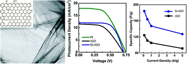
Heteroatom-doping of graphene is of fundamental importance to enable a wide range of optoelectronic and energy storage devices while exploring their basic material properties. Herein, a facile and low-cost method is presented to synthesize the silicon-doped reduced graphene oxide (Si-rGO) via annealing treatment of triphenylsilane and graphene oxide. Compared to the pristine reduced graphene oxide (rGO), Si-rGO exhibits significant enhancement in electrocatalytic and electrochemical properties: when Si-rGO is used as a metal-free electrocatalyst in counter electrodes in dye-sensitized solar cells (DSSCs), the conversion efficiency is increased by 29.6%; when Si-rGO is used as an active electrode in a supercapacitor, the specific capacity is increased by 48.5%. This suggests that silicon doping can effectively improve the electrocatalytic ability and electrochemical performance. It is promising for Si-rGO to be used as a metal-free catalytic and active material.
Besides the heteroatom doping mentioned above, theoretic research shows that the silicon doping can remarkably modulate the electronic structure and improve its physical/chemical properties.17–19 Chen and Niu demonstrated that silicon doped graphene could be an excellent candidate for metal-free sensors for the NO2 detection by theoretical and experimental investigations.20,21 Lv et al. reported that it can efficiently quench the fluorescence and enhance the Raman scattering of organic molecules.22 Just recently, our group demonstrated that the doping silicon into CVD graphene film could increase the hole concentration, and has relative higher mobility compared to other doped graphene.23 These investigations show that the silicon-doped graphene has various excellent properties, which will extend the applications of graphene-based materials. Furthermore, there are some reports about nitrogen-, boron- and/or sulfur doped or co-doped graphene for applications in DSSCs and supercapacitors.24–26 However, to the best of our knowledge, the application of silicon-doped graphene as metal-free counter electrodes in DSSCs and as active electrode materials in supercapacitors has not been explored yet.
In this study, we propose a facile, low-cost and scalable thermal annealing method for the synthesis of silicon-doped reduced graphene oxide (Si-rGO) using graphene oxide (GO) and triphenylsilane (C18H15Si) as carbon and silicon sources, respectively. Compared to undoped rGO, when Si-rGO acted as efficient metal-free electrocatalyst in counter electrodes in DSSCs, it demonstrates remarkable catalytic activity in I−/I3− redox reaction; when Si-rGO was employed as an active electrode material in supercapacitors, it exhibits significantly enhanced electrochemical properties compared to undoped rGO.
![]() | ||
Fig. 1 TEM (a) and SEM (b) images, EDX spectrum (c), and EDX element mapping of C (d) and Si (e) of Si-rGO. |
In order to further investigate the bonding configuration of Si atoms in Si-rGO, the XPS measurements were performed at room temperature. As shown in Fig. 2, compared to GO, the Si 2s and 2p peaks appear and the intensity of O 1s peak decreases in the XPS spectrum of Si-rGO. It indicates that the Si atoms are incorporated into rGO and the large amounts of oxygen-functional groups on GO are removed during the annealing treatment. It is noted that the possibility of physical adsorption of Si onto the samples is excluded by the following reasons. The samples were ultrasonically dispersed in various solvents of ethanol, acetone, ether and H2O; the XPS results reveal no change in the Si level before and after sonication. In addition, UV-vis and FTIR spectra of GO, rGO and Si-rGO were measured to confirm its reduction and shown in Fig. S2 and S3.† The high-resolution Si 2p XPS spectrum of Si-rGO was then collected to gain more insight into silicon doping. As shown in Fig. 2b, compared to rGO, there is an observable peak appearing in the range of 95–110 eV for Si-rGO, which originates from Si 2p. As for Si-rGO, the wider Si 2p XPS peak can be deconvoluted into three peaks at binding energies of 102.2, 103.0 and 103.9 eV, which correspond to the Si–C, C–Si–O and SiO2 bonds, respectively. This is similar with other group's results.21,22,27,28 By XPS elemental analysis, the total Si content (Si/C) in Si-rGO is 5.64 at%, in which Si–C/C, C–Si–O/C and SiO2/C are 1.66, 2.39 and 1.59%, respectively. Fig. 2c shows the high-resolution C 1s spectrum of Si-rGO. The C 1s peak can be deconvoluted into four peaks at binding energies of ∼284.7, 285.8, 287.5 and 289.9 eV, which correspond to C–C, C–O, CO and O–C
O, respectively. In addition, the oxygen content (O/C) of rGO and Si-rGO are 15.4 and 11.3 at%, respectively. This indicates that the silicon doping preferentially occurs at the sites of oxygen functional groups and affords a more effective reduction of GO, which is similar to that of P and S doping and reduction of GO.13,16 In addition, the effective reduction of GO will induce enhancement of carrier mobility of rGO.13,29 Due to the low amount of Si atoms, Si–C was hardly observed in corresponding C 1s XPS spectrum, and it might be overlaid with C–C.27,30 The XPS data strongly confirm that the silicon atoms are successfully incorporated into the graphene structure through a thermal annealing treatment.
![]() | ||
Fig. 2 XPS survey spectra (a), high-resolution spectra of Si 2p (b) and C1s (c) of Si-rGO and rGO, and the schematic structure of Si-rGO.17–20 |
Raman spectroscopy is an effective tool to investigate the doping effect of graphene. Fig. 3 presents the Raman spectra of GO, rGO, and Si-rGO. All samples exhibit D-bands (∼1350 cm−1) and G-bands (∼1580 cm−1), which are usually assigned to structural disorder and the graphitized structure, respectively.31 Fig. 3b shows corresponding ID/IG and the G-band position of such three samples. The intensity ratio ID/IG for the D-band and G-band is widely used for characterizing the defect quantity in graphene-based materials.32 As shown in Fig. 3b, compared to GO, the ID/IG of rGO and Si-rGO is higher, which is attributed to the decreased sp2 domains and the incomplete recovery of sp3 defects after reduction.33 The slight difference of rGO and Si-rGO may be related to the removal of the different functional groups upon reduction. The doped silicon atoms during reduction process also could affect ID/IG ratio.8,23 On the other hand, the G-band corresponds to the first-order scattering of the E2g mode of sp2 domain, and its position also corresponds to the change of carrier concentration with high sensitivity.31,34 As seen from Fig. 3b, compared to GO, the red shift (∼2.0 cm−1) the G-band of rGO was observed, which can be attributed to the reduction of GO, and such a shift has been reported in both chemical and thermal reductions of GO.11,35,36 Compared to rGO, the blue shift (∼7.0 cm−1) of the G-band in Raman spectra of Si-rGO was observed, which can be attributed to the silicon doping behaviour.23 Niu group's and our group's previous results show the silicon doping in graphene exhibits p-type doping behavior.21,23 Therefore, we can conclude that the blue shift of G-band reveals the increased hole concentration by silicon doping.
Many reports have demonstrated that heteroatom doping can effectively improve the electrochemical properties of rGO; however, to the best of our knowledge, the application of Si-rGO as metal-free counter electrodes in dye-sensitized solar cells (DSSCs) has not been explored yet. Therefore, we prepare DSSCs where Si-rGO was employed as active material in counter electrode. To decrease the experiment error, each sample has been employed to prepare 5 counter electrodes to get the average value and error bars. CV and EIS measurements were performed to understand the reaction kinetics and electrocatalytic properties of rGO, Si-rGO and Pt, as shown in Fig. 4a and b. It can be obviously observed one pair of reduction and oxidation peaks in all curves, which are attributed to the I3− reduction reaction and I− oxidation reaction, respectively.16,37 As is known, the higher reduction current density corresponds to the faster rate for I3− reduction. As shown in Table 1, the I3− reduction peak current density (Ireduction) is 0.87, 1.50 and 1.75 mA cm−2, corresponding to rGO, Si-rGO and Pt, respectively. Fig. 4b shows the EIS spectra, which is measured using DSH-23 as the electrolyte, and the equivalent circuit model used for fitting the resultant impedance spectra is illustrated in the inset of Fig. 4b. The charge-transfer resistance (Rct) is the resistance at the counter electrode/electrolyte interface for I3− reduction, and the lower Rct means the higher electrocatalytic activity. As shown in Table 1, after doping silicon, the Rct of rGO decrease from 9.37 to 5.42 Ω. This means that the Si-rGO counter electrode has higher electrocatalytic activity. Nevertheless, from Fig. 4b, one can see that the solution resistance (Rs) of Si-rGO (∼19.2 Ω) is much lower than that of rGO (∼43.2 Ω). This is due to the lower resistance of Si-rGO, which is originating from higher carrier mobility and higher hole concentration, which are confirmed with the XPS and Raman analysis. The CV and EIS measurements both show that Si-rGO can be used to realize I3− reduction, and its electrocatalytic activity is higher than that of rGO. Fig. 4c shows the photovoltaic properties of DSSCs employing rGO, Si-rGO and Pt counter electrodes. From Table 1, one can see that after doping silicon, the short-circuit photocurrent density (Isc) of DSSC increases from 11.66 to 12.06 mA cm−2 and the fill factor (FF) increases from 46.20% to 57.81%; however, the open-circuit voltage (Voc) has almost no change. Compare to rGO counter electrode, the conversion efficiency of Si-rGO counter electrode increases from 3.82% to 4.95%, which is increased by 29.6%. Compared to Pt counter electrode, the conversion efficiency of Si-rGO is lower, which may be results from the lower I3− reduction peak current density and higher charge-transfer resistance.
![]() | ||
Fig. 4 CV curves (a), EIS spectra (b) and photovoltage vs. photocurrent curves (c) of Si-rGO, rGO and Pt based counter electrodes. |
Ireduction (mA cm−2) | Rs (Ω) | Rct (Ω) | Isc (mA cm−2) | Voc (V) | FF (%) | η (%) | |
---|---|---|---|---|---|---|---|
rGO | 0.87 ± 0.07 | 43.21 ± 2.00 | 9.37 ± 0.71 | 11.66 ± 0.11 | 0.70 ± 0.10 | 46.20 ± 5.00 | 3.82 ± 0.12 |
Si-rGO | 1.50 ± 0.06 | 19.28 ± 2.10 | 5.42 ± 1.01 | 12.06 ± 0.15 | 0.71 ± 0.10 | 57.81 ± 4.00 | 4.95 ± 0.14 |
Pt | 1.75 ± 0.05 | 29.61 ± 1.50 | 3.21 ± 0.65 | 17.95 ± 0.11 | 0.74 ± 0.10 | 51.65 ± 4.00 | 6.86 ± 0.12 |
P-rGO16 | 1.64 ± 0.02 | 37.50 ± 1.60 | 3.28 ± 0.60 | 15.60 ± 0.13 | 0.74 ± 0.10 | 52.52 ± 5.00 | 6.04 ± 0.08 |
In our previous study,16 we reported the electrocatalytic of phosphorus-doped reduced graphene oxide (P-rGO) and the results were also shown in Table 1. Compared to P-rGO, Si-rGO has lower I3− reduction peak current density and higher charge-transfer resistance, and this leads to the conversion efficiency of Si-rGO is lower than that of P-rGO. This reveals that the enhanced ratio of electrocatalytic by doping silicon is lower than that of doping phosphorus, which may be due to the reduced barrier for I3− reduction, originating from the conjugation effect of the lone pair electrons on the phosphorus atoms and graphene π-system.38–40 In addition, the doping configuration of silicon, such as Si–O–C, and the existence of SiO2 nanoclusters will also give side effect on its properties. Nevertheless, compare to rGO, the Si-rGO has higher electrocatalytic properties, which demonstrates that doping silicon is also an effectively method to improve the electrocatalytic of rGO.
Furthermore, recent research shows that graphene-based double layer capacitors explore higher performance and is promising to be used in costumer electronic device.41 Recently, nitrogen-, boron- or phosphorus doped graphene has been used to fabricate supercapacitor and all of them show higher performance compared with pristine graphene.42,43 However, the use of silicon-doped graphene in supercapacitors has not been studied yet. A two-electrode system was first used to evaluate the electrochemical properties of Si-rGO. rGO was also tested using cyclic voltammograms techniques for comparison. Fig. 5a and b show the CVs of rGO and Si-rGO in 5.0 M KOH solution at various scan rates. As for Si-rGO, there is no remarkable peak in all of the curves, and the rectangular CV curves indicate the ideal double layer capacitor feature with a charge/discharge process. But for rGO, as shown in Fig. 5b, there is well-broadened peak in the range of 0.2–0.8 V, which indicates the presence of pseudo-capacitance.44 This might be due to the higher oxygen content of rGO. Fig. 5c shows the relationship between specific capacitance and current density, and the inset shows the galvanostatic charge/discharge curves of rGO and Si-rGO supercapacitors, where the current density is 0.1 A g−1. As seen, when the current density is 0.1 A g−1, the specific capacitance of Si-rGO is 184.4 F g−1, which is 48.5% larger than that of rGO (124.2 F g−1). The specific power density can be obtained from equations as following: SP = E/Δt, while E could be calculated by E = CV2/2, where the Δt is the discharge time. When the current density is 0.1 A g−1, the specific power densities are 101 and 107 kW kg−1, corresponding to rGO and Si-rGO. Further, when the current density increased to 5 A g−1, the specific capacitance of Si-rGO is still higher than that of rGO. It is well known that the performance of carbon-based nanostructures for supercapacitors is highly dependent on both the nanostructure and the conductivity. The more pore/defect is thus significant for providing rich sites for adsorbing ions and accelerating electron transfer or decreasing electric resistance loss.42,43,45 In this study, the silicon doping could break the basal plane of graphene and introduce more pore and also increase the concentration to enhance its conductivity. So we think that the higher specific capacitance is attributed to the more defect and the higher conductivity originating from silicon doping. Fig. 5d is the EIS spectrum of rGO and Si-rGO, which are measured in KOH solution. The electrode series resistance was derived from the high-frequency intersection of the Nyquist plot in the real axis. As seen, the series resistance of Si-rGO is lower than that of rGO, manifesting the low internal resistance of the Si-rGO. In low frequency region, both Si-rGO and rGO exhibited almost vertical line, indicating a nearly ideal capacitive behavior. Further, compare to rGO, the absence of the semicircle in Si-rGO demonstrated its high ionic conductivity at the electrode/electrolyte interface, which has also been observed in other reports.46,47 The charge-transfer resistance could be noted by the intersections of the curves in the low frequency region, and they are 0.61 and 2.89 Ω for Si-rGO and rGO. The lower charge-transfer resistance of Si-rGO reveals that silicon doping could effectively facilitate the charge transfer process, which may be originating from higher conductivity and more defect after doping silicon.47,48 The highly linear and symmetrical characteristic of charge/discharge curves, high specific capacitance of Si-rGO, make Si-rGO as a promising candidate in high-performance supercapacitors.
Footnote |
† Electronic supplementary information (ESI) available: TGA, UV-vis and FTIR spectra of samples. See DOI: 10.1039/c5ra25962b |
This journal is © The Royal Society of Chemistry 2016 |