Vapour phase nucleation of ZnO nanowires on GaN: growth habit, interface study and optical properties

C. Baratto*ab, M. Ferroniab, E. Cominiab, G. Fagliaab, S. Kaciulisc, S. K. Balijepallic and G. Sberveglieriab
aSensor Lab., CNR-INO Via Branze 45, 25133 Brescia, Italy. E-mail: camilla.baratto@unibs.it
bSensor Lab., University of Brescia, Dept. of Information Engineering, Via Branze 38, 25133 Brescia, Italy
c2CNR – ISMN, P. O. Box 10, Roma, 00015 Monterotondo Stazione, Italy

Received 25th November 2015 , Accepted 23rd January 2016

First published on 27th January 2016


Abstract

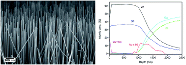
In the current work aligned ZnO nanowires were grown on p-GaN thin films for optoelectronic applications, using a vapour phase technique in a tubular furnace. To investigate the growth of ZnO nanowires at the interface with GaN, the heterojunction were characterized by scanning electron microscopy and X-ray photoelectron spectroscopy. Experimental evidence indicates that the Au catalyst remains at the interface between ZnO and GaN, and that interdiffusion of GaN into ZnO occurs. Concerning the ZnO growth, it starts with Vapour Liquid Solid (VLS) growth from Au catalyzer nanoparticles, then lateral growth takes place making nanowalls. After this initial stage, the nanowires both continue growth by VLS and start growing via a Vapour–Solid (VS) mechanism from the nanowalls. To investigate the potential of the heterostructure of ZnO nanowires on GaN as a light emitting diode, the device was also analysed by current–voltage characterization, photoluminescence and electroluminescence spectroscopy.


1. Introduction

Nanostructures of zinc oxide (ZnO), a material featuring a 3.37 eV band gap and a 60 meV exciton binding energy at room temperature, are of considerable interest for ultraviolet/blue optoelectronic applications.1,2 ZnO shows emission in the UV at 3.28 eV and in the visible region (green to orange): the emission in the UV is due to excitonic recombination, while the visible emission depends on the preparation conditions and is generally attributed to defects.3–7 Thanks to its large exciton emission in the UV and lower Auger recombination (i.e. lower efficiency drop at high current density),8 ZnO represents a promising indium-free alternative to III-nitride light emitting diodes (LED).

Due to the difficulties in producing p-type ZnO, the most promising approach is to prepare the heterojunction with p-type semiconductors matching bands and lattice. The optimal choice of p-type material for efficient hole injection in the n-type ZnO regions is p-type GaN.9 LED based on ZnO thin films/GaN thin films have been already demonstrated, but an increase in device efficiency is demonstrated when nanowires are employed instead of thin films.10,11 Nanowires ensure a high degree of crystallinity of the ZnO material;12 moreover, the defect free wires show the waveguiding effect,13 when the nanowires are aligned perpendicular to the surface: this helps to extract the photons generated at the ZnO/GaN interface. Growing ZnO nanowires on GaN takes advantage of the same wurtzite structure of ZnO and GaN with a relatively small mismatch in the lattice constant and a much lower growth strain compared to thin films. ZnO nanowires shows good transparency in the visible range and energy gap similar to the one reported for bulk material.14,15

Vapour phase growth technique does not require toxic precursors or keep traces of solvents and precursors and provides a relatively inexpensive route for nanowires fabrication: by changing the pressure, temperature and precursor we were able to grow high-quality ZnO nanowires (NWs) on Si, alumina and sapphire substrates.16 When using GaN substrates on sapphire, we were able to tailor the deposition conditions to obtain a dense growth of nanowires aligned perpendicular to the surface.17

Instead of focusing only on the emission properties of the heterojunction ZnO nanowires/GaN, widely reported in literature,11,18,19 our aim is to study the growth habit of ZnO nanowires and the interface GaN/ZnO to have insight into the emission properties of the device. Despite the importance that the interface deserves for realizing an emitting device, this topic has been seldom addressed: Levin et al. have studied growth habit and defects in ref. 20, but no reference to the emission properties was drawn. This information is of great importance, since the defects at the interface can prevent the radiative recombination responsible of light emission. In the present study the interface between ZnO NW and thin film of p-GaN was investigated by scanning electron microscopy (SEM) and X-ray Photoelectron Spectroscopy (XPS) techniques. The heterojunction properties were investigated by current–voltage analyses, photoluminescence (PL) and electroluminescence (EL) spectroscopy.

2. Experimental details

2.1. ZnO nanowires growth

ZnO nanowires were prepared by vapour phase growth technique in an evacuated tubular furnace. As a substrate we used GaN templates provided by OSRAM Opto Semiconductors. These consist of a magnesium doped p-GaN layer (100 nm thick, Mg concentration is about 1020 cm−3) connected to an underlying 6 μm thick n-type GaN[thin space (1/6-em)]:[thin space (1/6-em)]Si layer by a tunnel junction providing an ohmic contact.

Several experiments were performed to understand the parameters required to obtain an effective growth of nanowires on GaN thin films. In high temperature growth, the use of a catalyser or a seed layer is mandatory for a dense growth of nanowires. In vapour liquid solid (VLS) growth, Au is the most frequently used catalyser,21 followed by Pt. When the growth cycle was conducted without any catalyst, the density of ZnO nanowires was not sufficient to cover the GaN thin film. Before nanowires growth, the surface of p-GaN was cleaned in HF, and then Au catalytic nanoparticles were deposited by RF sputtering at 50 W and at 6 × 10⁻³ mbar for 5 s. The deposited Au layer converts into Au droplets after thermal treatment during deposition. The dimension of the Au droplets is ranging between 10 and 40 nm in diameter (see ESI Fig. 2). The amount of gold deposited was optimized to obtain dense nanowire growth. After the deposition of the catalyst, the substrates were positioned into the furnace at the temperatures of 580–640 °C, zinc oxide powder is placed at 1370 °C and the deposition is performed at a pressure of 100 mbar, with 100 sccm of argon as a gas carrier to ease the mass transport. More details on the growth technique on different substrates (alumina, silicon) have been already reported elsewhere.15

Two types of samples were considered for this study: one with ZnO growth duration of 5 min (named in the following as ZnO-5) and the other with growth duration of 15 min (ZnO-15).

To study the emission properties of the heterojunction, we prepared a sample deposited for 15 minutes as for ZNO-15, then polymethyl-methacrylate (PMMA) was spin-coated on ZnO nanowire region, to act as an insulating layer to prevent short circuit between the top electrode and p-GaN thin film. To remove the PMMA from the tip of the nanowires, a plasma etching treatment in Ar was performed in a custom made system (Colibrì – Gambetti) with parallel plate electrodes. As a final step, Au contacts were deposited by RF sputtering on ZnO and GaN.

2.2. Scanning electron microscopy

SEM analysis was carried out by using a field emission LEO 1525 scanning electron microscope, operated at 5 keV to prevent electrostatic charging of the specimen. Neither carbon or gold was deposited over the specimen; the In-Lens and BSE detectors for secondary-electrons and backscattered-electrons imaging was used for planar and cross-sectional view. The cross-sections of the specimens were prepared to investigate the interface between the GaN substrate and the ZnO deposited nanostructures. Different approaches were used to avoid artefacts arising from the sectioning of the delicate ZnO layer. Preliminary, the sections were uncovered by cleavage of the GaN substrate. To prevent the nanowires from detaching or breaking under cleavage, the ZnO layer was protected and reinforced with epoxy before sectioning. Eventually, the specimen was embedded in a glued stack to allow a gentle polishing with 1 μm grit-size diamond paste.

2.3. XPS analysis

XPS analysis and depth profiling by cyclic ion sputtering were carried out in an ESCALAB 250Xi spectrometer (Thermo Fisher Scientific, UK), equipped with monochromatic Al Kα excitation source, electron and ion flood guns for charge neutralization and a 6-channeltron spectroscopic detection system. Photoelectron spectra were collected at 40 eV constant pass energy of the analyser (0.72 eV resolution in energy) and in electromagnetic lens mode resulting in 0.3 mm diameter of analysed sample area. A base pressure in the analysis chamber of about 5 × 10⁻⁸ Pa was increased up to 1 × 10⁻⁵ Pa for the ion sputtering with differentially pumped ion gun, an EX-06. For the depth profiling an Ar+ beam of 1.0 keV energy and 3 × 10⁻⁶ A sample current was employed; the beam was rastered over a sample area of 1 × 1 mm2. The average sputtering rate for ZnO was about 0.9 nm s−1. This value was calculated from the value measured on the reference sample of Ta2O5 film, by taking into account the sputtering rates for Zn and Ta from reference table. All spectroscopic data were processed by using the Avantage v.5 software. The peak fitting was carried out by using Shirley background and a 30% mixture of Gaussian and Lorentzian functions.

2.4. Electrical and optical characterization

Current–voltage (IV) curves were acquired using a Keithley 2410 source meter. Continuous-wave PL and EL characterization were carried out at room temperature in a macro configuration using a He–Cd laser as light source at 325 nm. PL spectra were acquired at incidence normal to the surface of the samples using a single spectrograph and a Peltier cooled CCD detector (Acton). A wedge filter was used to get rid of Rayleigh line.

3. Results and discussions

3.1. SEM characterization of the ZnO nanowires

We investigated the morphological properties of ZnO-5 and ZnO-15 samples from the plan and cross-sectional SEM observations.

Fig. 1 reports the morphology of the ZnO sample after 5 min deposition. The plan view (a) highlights the formation of a complicated basal structure, owing to the connection between the nucleation structures. Despite the proximity of the structures, the network is formed by lamellar structures, which are nearly constant in width (nanowalls). The additional side view in Fig. 1(b) reveals that thin nanowires emerge from the underlying network. The lateral size of the nanowire is controlled by the underlying lamellar structure, with an average value of 45 nm. The section on the nanowires resulted shorter when measured transversally across the lamellar structure, than parallel to it: average values of 37 and 54 nm were measured respectively. Most of the nanowires are vertically oriented; together with the homogeneity of the basal structure, this is and indication that some degree of crystalline orientation is preserved during the growth.


image file: c5ra25019f-f1.tif
Fig. 1 Top-(a) and side-(b) views of the ZnO-5 sample. The basal ZnO structure and the standing nanowires are well distributed and aligned.

Fig. 2 shows the ZnO-15 sample. The combination of the basal network and the standing aligned nanowires is similar to the one observed in the previous sample, but there is evidence of increased density of nanowires. The top view highlights a large number of nanowires nucleated from the underlying network. The lateral dimension of the lamellar structure is similar to that of ZnO-5 sample, indicating that the growth prolongation does not increase it. The dimension of the basal ZnO structure is most probably determined by the size and distribution of the Au nanoparticles, which was the same for ZnO-5 and ZnO-15 samples.


image file: c5ra25019f-f2.tif
Fig. 2 Top-(a) and side-(b) views of the ZnO-15 sample. The nanowires stand aligned over the basal structure.

The cross sectional observation of the samples revealed some insight into the ZnO nanostructure (Fig. 3). The backscattered electrons image of the cross section reveals that a layer of Au nanoparticles is present between the ZnO material and the GaN substrate. This evidence holds for both samples.


image file: c5ra25019f-f3.tif
Fig. 3 SEM cross section of the ZnO-5 (a) and ZnO-15 (b) samples. The catalyst Au nanoparticles are visible in both samples, between the lamellar basal ZnO structure and the GaN substrate.

For longer growth time (ZnO-15) a thinner layer of Au nanoparticles is observed, indicating that Au is consumed as the deposition time increases. At the growth beginning, a VLS mechanism of growth is hypothesized, with the Au nanoparticle that remains at the bottom of the nanowires (root growth), as reported in other works.22 The incorporation of the growth material into the catalytic particle may change the volume and thus the diameter of the particle from its initial size, explaining the dimension of the basal structure having constant width around 45 nm, with respect to the 10 nm to 40 nm diameter observed for Au nanoparticles. The aligned ZnO nanowires growing on the top of the basal structure indicate – on the contrary – a mechanism of vapour–solid (VS) growth where the nanowires nucleate from defects in the basal ZnO network, instead of being driven by ZnO crystallization at the supersaturated Zn–Au catalytic nanoparticle. Probably the two mechanisms coexist in our process. As reported by Levin et al.,20 some residual strain and also presence of stacking faults at the (0001) planes can be expected in the basal structure, while ZnO nanowires could be considered free from strain and with single-crystalline ordering.

A scheme of the growth process based on the SEM observation is proposed in Fig. 4. The dispersion of gold nanoparticles in Fig. 4(a) has been depicted starting from SEM image of the layer of Au nanoparticles used as a catalyser (see ESI Fig. 2(a)). If the first step of growth occurs by VLS mechanism, nanowires starts where the gold particles are, by root growth (Fig. 4(b)); then the diameter of the nanowires slightly increases to match the diameter of the catalyst particle and lateral growth of nanowalls occurs – Fig. 4(c) – creating connection between rods that makes up the observed basal structure; at the same time vertically aligned nanowires extrudes from the basal structure – Fig. 4(d). The nanowires protruding from the basal structure could be both the prolongation of the nanowires grown by VLS mechanism and new nanowires grown from nanowalls by VS mechanism. This second mechanism is supported by the observation of increased density of nanowires in samples grown for longer time (Fig. 2).


image file: c5ra25019f-f4.tif
Fig. 4 Scheme of the growth process (top view and side view): (a) gold clusters on GaN thin films; (b) thin nanowires starts growing on each gold cluster by VLS process; (c) dimension of the nanowires increases to the dimension of the gold cluster and lateral growth of ZnO occurs, connecting the nanowires into a “basal network”: nanowalls growth; (d) the length of nanowires increases with growth time and they extrudes from the basal structure. For the sake of clarity the underlying gold particles are not represented in (c) and (b) top view.

As a result, part of the Au used to promote the ZnO growth is not consumed and remains at the bottom of the ZnO basal structure, as observed in Fig. 3.

3.2. XPS characterization

To study the interface between GaN and ZnO nanowires we used XPS. This analysis was performed on ZnO-5 and ZnO-15 samples. Since our aim was to study the interface between ZnO nanowires and GaN, the thinner ZnO-5 sample was selected to be shown in the XPS discussion. The XPS characterization of ZnO-15 sample was very similar to that of ZnO-5, being the only difference the higher thickness of ZnO nanowire layer.

On the surface of the as-prepared sample (i.e., before ion sputtering) we observed stoichiometric ZnO with total atomic ratio Zn[thin space (1/6-em)]:[thin space (1/6-em)]O = 1 and Auger parameter of Zn α′ = 2010 eV. The spectral regions of Zn 2p (binding energy BE = 1021.8 eV) and Zn LMM (kinetic energy KE = 988.2 eV) peaks are shown in Fig. 5(a) and (b), respectively. The value of Auger parameter and the shape of these spectra and both the values of BE and KE are in good agreement with literature data for ZnO.23 In addition, on the surface are also present the significant components of hydroxyl groups O2 (adsorbed and/or bonded in zinc hydroxide) and adsorbed water O3,24 that were revealed from the peak fitting of O 1s spectrum illustrated in Fig. 5(c).


image file: c5ra25019f-f5.tif
Fig. 5 Zn 2p (a) and Zn LMM (b) spectra of the ZnO-5 sample. (c) O 1s spectrum of the ZnO-5 sample before XPS depth profiling on as prepared ZnO-5 sample. Synthetic components: O1–Zn oxide, O2–hydroxide and/or adsorbed OH– groups, O3–adsorbed water. (d): XPS depth profile of the ZnO-5 sample acquired by using Ar+ sputtering at 1.0 keV energy.

The results of XPS depth profiling are reported in Fig. 5(d). After the first cycle of ion sputtering (t = 100 s), the components of hydroxyl groups (O2) and water (O3) disappeared and the ratio Zn[thin space (1/6-em)]:[thin space (1/6-em)]O becomes about 1.7–1.8, i.e. it is nearer to the stoichiometry of Zn2O. However, the value the Auger parameter remains constant during the depth profile, indicating the same chemical state of Zn, whereas the different stoichiometry could be caused by the effect of preferential sputtering of oxygen observed by XPS in other metal oxides.25,26 Beside ZnO stoichiometry of sample ZnO-5 was further confirmed by XRD analysis (see ESI, Fig. 1). The presence of oxygen defects at the interface cannot be excluded basing only on XPS results.

At the interface between ZnO nanowires and GaN film, the Au 4f signal was observed, that is in agreement with the observation of SEM reported in Fig. 3. It should be noted, that the interface ZnO/GaN appears very wide in the XPS profile, but this can be easily explained by the nanowires morphology and the depth profiling procedure. During depth profiling, the ion sputtering is performed at 50° angle on the forest of nanowires with different lengths. When Au, Ga and N signal start to appear, the signal of ZnO can be still be present, due to the non-uniform erosion of the nanowires under ion sputtering. The real interface can be thinner than that observed by XPS.

Given the uncertainty in the dimension of the interface, the thickness of ZnO nanowire and basal structure (including also the interface with Au particles and GaN) can be estimated to be about 1200 nm, in agreement with data from SEM image (Fig. 3(a)). Au particles, present at the interface with GaN, are characterized by a low atomic concentration of about 0.2%.

From XPS data, we can affirm that the diffusion of ZnO into GaN is very probable. Even if we consider the apparent broadness of the interface, still the signals of Zn and O protract very deep into the region of GaN. It is not possible to suspect the presence of some different phase or stoichiometry of ZnO in the interface region, because the peaks of Zn 2p and O 1s maintain the constant shape, BE values and atomic ratio. Literature also reports the diffusion of Zn in the GaN layer in Ga doped ZnO thin film/GaN interface after a thermal treatment at 800 °C.27

Summarizing the results of XPS and SEM characterization, there is the evidence of Au presence at the interface between GaN and ZnO, whereas gold particles are not detected at the tip of the nanowires. These particles can act as trap states for carriers, and together with interdiffusion of ZnO into GaN can be detrimental for electroluminescence process at the ZnO/GaN junction. The Au particles can be hindered under the lamellar structure of ZnO.

3.3. IV, photoluminescence and electroluminescence spectroscopy

To study the emitting properties of the junction IV characterization, photoluminescence and electroluminescence spectroscopy were employed. Fig. 6(a) reports IV tests on the junction acquired in the range (−2 V; +2 V). The bias range was chosen in a way to keep the current lower than 10−2 A, the maximum current readable by the Keitheley 2410. Fig. 6(a) reports the scheme of the device. Poor rectifying behaviour observed could be due either to gold particles or to ZnO–GaN interdiffusion.
image file: c5ra25019f-f6.tif
Fig. 6 (a) IV curve between ZnO nanowires and GaN; (b) a scheme of the device; (c) PL spectra of ZnO nanowires and GaN thin film (dotted lines) and EL spectra of junction in reverse bias at 8 V, 10 V and 11 V (continuous lines). PL spectra of ZnO and GaN were divided by a factor of 10 to be compared to the EL data.

Fig. 6(c) reports PL and EL spectra of the device; for better comparison, PL spectra were divided by a factor of 10. PL spectrum of ZnO nanowires (ZnO-15/blue line), is dominated by Near Band Edge (NBE) exciton emission of ZnO in the UV at 3.26 eV; this express the high quality of the prepared nanowires. Emission from defects in the green region can be observed with a broad peak, centred at 2.4 eV. The origin of green emission in ZnO nanowires is still debated: the defect involved could be a single ionized oxygen vacancy,4 an antisite oxygen,6 donor–acceptor complexes,28 or interstitial Zn.29 No emission from the underlying GaN thin film can be observed, due to complete coverage of the GaN template by the nanowires.

PL spectrum of GaN template (violet line), shows a very small peak at 3.39 eV (free exciton recombination emission), along with emission in the blue at 2.8 eV, related to Mg doping of GaN30 and yellow luminescence at 2.21 eV, typically observed in Si doped GaN, probably due to emission from n-GaN layer.31

Electroluminescence spectra were acquired in the same experimental setup, biasing the heterojunction in forward and in reverse bias from 1 to 15 V. No electroluminescence in the UV or visible region from the heterojunction in forward bias has been observed. When biased in reverse configuration, emission in the yellow-orange region was observed starting from 8 V. Turn on voltage, defined as the minimum voltage applied to observe an emission, is thus 8 V. At 11 V an emission in the blue region is observed around 3 eV. Such emission is reported in literature for ZnO layers and ascribed to the radiative emission from Zni defects.32 At bias greater than 11 V, the current flowing into the junction heats the device by Joule heating, irreversibly damaging the device.

In reverse bias, the EL mechanism is different from that of conventional forward – biased p–n junction light emitting diodes.33 Park and Yi34 proposed that in reverse bias carrier transport is explained in terms of band alignment of p-GaN/n-ZnO heterojunction at the interface, as a result of electron transport involving tunnelling through the heterojunction. The yellow-orange and blue emission observed in our work can possibly be ascribed to a defective interface, that also prevented emission in the UV.

4. Conclusions

Aligned ZnO nanowires were grown by vapour phase technique on GaN thin film for LED application. Dense growth of nanowires was obtained in presence of Au catalyst, which served as a nucleation centre for ZnO. As the growth time increased, the connection between the nucleation structures was observed, resulting in the formation of a complicated basal structure with lamellar walls of constant width. In addition, thin vertically oriented nanowires emerged from the underlying network. The diameter of the nanowires was controlled by the width of the underlying lamellar structure, and the lateral dimension of the lamellar structure did not depend on the growing time. From cross sectional view, Au catalyst nanoparticles at the interface between ZnO and GaN were observed. This is further confirmed by XPS analysis, which revealed the presence of Au at the interface. From XPS data, interdiffusion of GaN into ZnO cannot be excluded.

The functional properties of the studied heterojunction are in agreement with results obtained by SEM and XPS. PL spectrum of ZnO nanowires showed bright PL spectrum typical of high quality nanowires with exciton emission in the UV emerging over the one in the visible attributable to defects. The lack of GaN peaks in the spectrum acquired in ZnO nanowires region further assessed the density of nanowires. As expected from the analysis of the interface, IV curve showed poorly rectifying characteristics; EL emission in the yellow-orange and blue region can be observed only in reverse bias. Defective interface can play a role in determining no emission in the UV region.

Acknowledgements

The research leading to these results has received funding from the European Communities 7th Framework Programme under grant agreement NMP3-LA-2010-246334 ORAMA (Oxide Materials Towards a Matured Post-silicon Electronics Era). Financial support of the European Commission is therefore gratefully acknowledged. The research project “WIROX” Oxide Nanostructures for Wireless Chemical Sensing, PEOPLE MARIE CURIE ACTIONS, International Research Staff Exchange Scheme PIRSES-GA-2011-295216, Call: FP7-PEOPLE-2011-IRSES, 2012–2015 is also acknowledged. In addition the authors thank OSRAM Opto-Semiconductors for providing the GaN templates within the ORAMA project.

Notes and references

  1. J. M. Bao, M. A. Zimmler, F. Capasso, X. W. Wang and Z. F. Ren, Nano Lett., 2006, 6, 1719–1722 CrossRef CAS PubMed.
  2. M. H. Huang, S. Mao, H. Feick, H. Q. Yan, Y. Y. Wu, H. Kind, E. Weber, R. Russo and P. D. Yang, Science, 2001, 292, 1897–1899 CrossRef CAS PubMed.
  3. J. D. Prades, A. Cirera, J. R. Morante and A. Comet, Thin Solid Films, 2007, 515, 8670–8673 CrossRef CAS.
  4. K. Vanheusden, W. L. Warren, C. H. Seager, D. R. Tallant, J. A. Voigt and B. E. Gnade, J. Appl. Phys., 1996, 79, 7983–7990 CrossRef CAS.
  5. A. van Dijken, E. A. Meulenkamp, D. Vanmaekelbergh and A. Meijerink, J. Lumin., 2000, 87–9, 454–456 CrossRef.
  6. J. Q. Hu and Y. Bando, Appl. Phys. Lett., 2003, 82, 1401–1403 CrossRef CAS.
  7. S. A. Studenikin and M. Cocivera, J. Appl. Phys., 2002, 91, 5060–5065 CrossRef CAS.
  8. M. Heinemann and C. Heiliger, J. Appl. Phys., 2011, 110, 083103 CrossRef.
  9. C. Soldano, E. Comini, C. Baratto, M. Ferroni, G. Faglia and G. Sberveglieri, J. Am. Ceram. Soc., 2012, 95, 831–850 CAS.
  10. S. Xu, C. Xu, Y. Liu, Y. F. Hu, R. S. Yang, Q. Yang, J. H. Ryou, H. J. Kim, Z. Lochner, S. Choi, R. Dupuis and Z. L. Wang, Adv. Mater., 2010, 22, 4749–4753 CrossRef CAS PubMed.
  11. X. M. Zhang, M. Y. Lu, Y. Zhang, L. J. Chen and Z. L. Wang, Adv. Mater., 2009, 21, 2767–2770 CrossRef CAS.
  12. R. Guo, J. Nishimura, M. Matsumoto, M. Higashihata, D. Nakamura and T. Okada, Appl. Phys. B: Lasers Opt., 2009, 94, 33–38 CrossRef CAS.
  13. M. A. Zimmler, J. Bao, F. Capasso, S. Muller and C. Ronning, Appl. Phys. Lett., 2008, 93, 051101 CrossRef.
  14. H. E. Unalan, P. Hiralal, N. Rupesinghe, S. Dalal, W. I. Milne and G. A. J. Amaratunga, Nanotechnology, 2008, 19 Search PubMed.
  15. S. N. F. Hasim, M. A. A. Hamid, R. Shamsudin and A. Jalar, J. Phys. Chem. Solids, 2009, 70, 1501–1504 CrossRef.
  16. C. Baratto, E. Comini, M. Ferroni, G. Faglia and G. Sberveglieri, Crystengcomm, 2013, 15, 7981–7986 RSC.
  17. C. Baratto, R. Kumar, E. Comini, G. Faglia and G. Sberveglieri, Opt. Express, 2015, 23, 18937–18942 CrossRef CAS PubMed.
  18. S. Jha, J. C. Qian, O. Kutsay, J. Kovac, C. Y. Luan, J. A. Zapien, W. J. Zhang, S. T. Lee and I. Bello, Nanotechnology, 2011, 22 Search PubMed.
  19. O. Lupan, T. Pauporte and B. Viana, Adv. Mater., 2010, 22, 3298–3302 CrossRef CAS PubMed.
  20. I. Levin, A. Davydov, B. Nikoobakht, N. Sanford and P. Mogilevsky, Appl. Phys. Lett., 2005, 87, 103110 CrossRef.
  21. X. D. Wang, J. H. Song, C. J. Summers, J. H. Ryou, P. Li, R. D. Dupuis and Z. L. Wang, J. Phys. Chem. B, 2006, 110, 7720–7724 CrossRef CAS PubMed.
  22. K. W. Kolasinski, Curr. Opin. Solid State Mater. Sci., 2006, 10, 182–191 CrossRef CAS.
  23. S. Kaciulis, L. Pandolfi, E. Comini, G. Faglia, M. Ferroni, G. Sberveglieri, S. Kandasamy, M. Shafiei and W. Wlodarski, Surf. Interface Anal., 2008, 40, 575–578 CrossRef CAS.
  24. S. Kaciulis, G. Mattogno, A. Galdikas, A. Mironas and A. Setkus, J. Vac. Sci. Technol., A, 1996, 14, 3164–3168 CAS.
  25. S. Kaciulis and G. Mattogno, Surf. Interface Anal., 2000, 30, 502–506 CrossRef CAS.
  26. S. Kaciulis, L. Pandolfi, S. Viticoli, G. Sberveglieri, E. Zampiceni, W. Wlodarski, K. Galatsis and Y. X. Li, Surf. Interface Anal., 2002, 34, 672–676 CrossRef CAS.
  27. R. H. Horng, K. C. Shen, C. Y. Yin, C. Y. Huang and D. S. Wuu, Opt. Express, 2013, 21, 14452–14457 CrossRef CAS PubMed.
  28. B. X. Lin, Z. X. Fu and Y. B. Jia, Appl. Phys. Lett., 2001, 79, 943–945 CrossRef CAS.
  29. T. Tatsumi, M. Fujita, N. Kawamoto, M. Sasajima and Y. Horikoshi, Jpn. J. Appl. Phys., Part 1, 2004, 43, 2602–2606 CrossRef CAS.
  30. U. Kaufmann, M. Kunzer, M. Maier, H. Obloh, A. Ramakrishnan, B. Santic and P. Schlotter, Appl. Phys. Lett., 1998, 72, 1326–1328 CrossRef CAS.
  31. U. Kaufmann, M. Kunzer, H. Obloh, M. Maier, C. Manz, A. Ramakrishnan and B. Santic, Phys. Rev. B: Condens. Matter Mater. Phys., 1999, 59, 5561–5567 CrossRef CAS.
  32. C. H. Ahn, Y. Y. Kim, D. C. Kim, S. K. Mohanta and H. K. Cho, J. Appl. Phys., 2009, 105 Search PubMed.
  33. X. Y. Chen, A. M. C. Ng, F. Fang, A. B. Djurisic, W. K. Chan, H. L. Tam, K. W. Cheah, P. W. K. Fong, H. F. Lui and C. Surya, J. Electrochem. Soc., 2010, 157, H308–H311 CrossRef CAS.
  34. W. I. Park and G. C. Yi, Adv. Mater., 2004, 16, 87–90 CrossRef CAS.

Footnote

Electronic supplementary information (ESI) available. See DOI: 10.1039/c5ra25019f

This journal is © The Royal Society of Chemistry 2016
Click here to see how this site uses Cookies. View our privacy policy here.