S. J. Sitler* and
K. S. Raja
University of Idaho, Department of Chemical and Materials Engineering, Moscow, Idaho 83844, USA. E-mail: Sitl1428@vandals.uidaho.edu
First published on 22nd January 2016
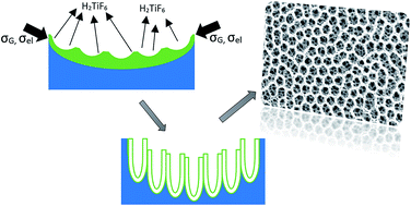
A new method for creating a honeycomb morphology of TiO2 nanotubular arrays has been proposed using a two-step anodization process. The first anodization step utilizes fluoride containing ethylene glycol as an electrolyte (EG-solution). The anodic oxide formed during the first anodization step was removed to expose hemispherical nanoindentations created on the substrate. These nanoimprints acted as templates for honeycomb morphology during the second step of anodization that was carried out in fluoride containing phosphoric acid solution (PA-solution). Several small diameter nanotubes were grown in each honeycomb cell during the second anodization step. The formation of such honeycomb morphology required a threshold concentration of Ti4+ in the anodization electrolyte. Below the threshold Ti4+ concentration (4 × 10⁻³ M in this investigation), a good honeycomb morphology was not observed. The formation mechanism proposed is based on weakly linear surface perturbation theory aided by compressive growth stresses and a decrease in surface energy due to the presence of [TiF6]2− species.
The two-step anodization method has also been employed to obtain highly ordered TiO2 nanotubular arrays by mechanically removing the first anodized layer and growing the well-ordered oxide nanotubes by the second anodization. The ordered hemispherical imprints, also called scalloped imprints, left by the first anodization process on the titanium substrate served as templates for the perfect alignment of the subsequent anodization process.31 Furthermore, the two-step anodization method has been used for fabrication of open-ended TiO2 nanotube arrays.32
Normally, in order to achieve a highly ordered TiO2 nanotubular array, the first and second anodization steps are carried out under similar experimental conditions in a fluoride containing organic solvent with about 2.5% water addition and without changing the anodization potential.33 When the second anodization is carried out at a lower potential than that of the first anodization step, several smaller diameter nanotubes form within the larger scallop imprint of the first anodization revealing a honeycomb or lotus root like morphology.34
In this investigation, a honeycomb like morphology of TiO2 nanotubular arrays has been developed through a two-step anodization process using two different electrolytes and anodization parameters. Fluoride containing organic solvent was used as the electrolyte in the first anodization process and an aqueous acidic solution containing fluoride was used in the second anodization process. A critical concentration of Ti4+ was required in the electrolyte to form the honeycomb structure during the second anodization process. The formation mechanism of the honeycomb like morphology has been discussed based on the perturbation of dielectric interfaces under an electric field and capillary forces.
After anodization, select samples were thermally annealed at 450 °C for 2 hours in air. The heating and cooling rates for thermal annealing were controlled at 5 °C min−1. A Shimadzu UV-2401PC spectrometer equipped with a tungsten lamp was used to obtain the optical absorbance spectra based on the diffuse-reflectance of the samples. The absorbance was recorded by scanning the light wavelength from 250 to 900 nm with a step size of 1 nm. A Thermo-Scientific DXR dispersive Raman microscope was utilized to obtain the vibrational spectra of the sample surfaces. Samples were analysed using a laser of 532 nm in wavelength at 5 mW power, a 0.7 μm spot size, and an exposure time of 5 seconds. The reported results were the average of 32 exposures. X-ray diffraction was performed using a Rigaku Smartlab diffractometer with Cu Kα wavelength of 1.54 Å, operated at 44 kV, 40 mA, and scanning in the 2θ range from 20° to 90°.
![]() | ||
Fig. 2 Titanium nanoindented surface after removal of oxide layer as seen in Fig. 1. |
The second anodization step carried out in an aqueous fluoride solution at 20 V for 40 minutes resulted in two different morphologies depending on the initial concentration of the Ti4+ ions in the electrolyte. If the second anodization was carried out in a freshly prepared PA-solution (0.5 M H3PO4 + 0.14 M NaF), then the anodic oxide showed a regular TiO2 nanotubular morphology as shown in Fig. 3(a) and (b). During this second step of anodization, the oxide nanotubes were grown beneath the scalloped layer. The diameter of these second anodized nanotubes was in the range of 80–100 nm. Since both the electrolyte and the potential were different in this step, the diameter of the nanotubes was different from that of the nanopattern. Therefore, the ordering of the nanotubular array did not improve significantly as compared to the results reported in the literature.35 Fig. 3(b) shows the side view of the anodic oxide formed during this second anodization step, where the vertical orientation of the nanotubes can be clearly seen along with the formation of nanoindentation patterns on the titanium foil due to the second anodization step.
![]() | ||
Fig. 3 SEM image of regular TiO2 nanotubes produced from two-step anodization. (a) Planar view (b) cracked side view also revealing indented titanium substrate. |
When the second step of anodization was carried out in an aged solution, a different morphology, referred to as ‘honeycomb’ structure, where each hemispherical nanoindentation contained multiple smaller nanotubes, was observed. Here, the aging of the solution is referred to the use of the same PA-solution multiple times with a titanium cathode to dissolve Ti4+ into the PA-solution for anodization. In a typical anodization, 300 ml of PA-solution was used for anodizing 2 cm2 area of the titanium coupon for 40 minutes. During the anodization, the following reactions are proposed to take place at the anode:
Ti → Ti4+ + 4e− | (1) |
Ti4+ + 4H2O → Ti(OH)4 + 4H+ | (2) |
Ti(OH)4 → TiO2 + 2H2O | (3) |
TiO2 + 6H+ + 6F− → H2TiF6 + 2H2O | (4) |
Ti4+ + 6F− → [TiF6]2− | (5) |
If the solution was used again for anodization, then accumulation of [TiF6]2− ions would occur. Presence of these [TiF6]2− ions in critical concentration was observed to be essential for formation of the honeycomb structured nanotubular arrays. Li et al.33 also reported the role of aging of the electrolyte, but did not give the value of critical concentration of the [TiF6]2− species, or state if that was the desired effect of aging the solutions. These authors also pointed out that their honeycomb morphology required reduction in the voltage during the second step of anodization. Similar observations were also made by Wu et al.34 The reason for not reporting a critical concentration of [TiF6]2− could be that these researchers carried out the first and second anodization steps in the same electrolyte, though not mentioned explicitly. This present investigation is different from their work because a totally different type of electrolyte was used for the second anodization step and therefore a critical concentration of [TiF6]2− was required to obtain the honeycomb morphology. In this study, the PA-solution was used multiple times, the first anodization run did not reveal any honeycomb like structure as can be seen in Fig. 3(a). When the PA-solution was used for second time, the honeycomb pattern started to appear, where the multiple nanotubes having diameter much smaller than that of the hemispherical nanoindentations formed inside each honeycomb as seen in Fig. 4. It was observed that the outline of the honeycomb morphology formed by the boundaries of the hemispherical nanoindentations.
Based on this observation, it is interpreted that a threshold concentration of [TiF6]2− ions or Ti4+ ions was required to initiate the honeycomb like structure. Therefore, different known concentrations of [TiF6]2− ions were added in the PA-solution before starting the second anodization step. This was carried out by dissolving titanium foil in the PA-solution (0.5 M H3PO4 + 0.14 M NaF) for various times and monitoring the weight loss of the titanium foil as a function of time. It should be noted that titanium foil corrodes in the PA-solution at open circuit potentials. This corrosion process introduced [TiF6]2− ions into the solution. The PA-solution with different concentrations of Ti4+ in the range of 0–6.26 × 10⁻³ M (corresponding to 0–0.3 g of titanium in 1 liter) was used for the second step of anodization. It was observed that the honeycomb morphology started to appear when the concentration of Ti4+ in the form of [TiF6]2− ions was 2 × 10⁻³ M, similar to that shown in Fig. 4. Highly ordered nanopores contained in a honeycomb structure were obtained when the PA-solution was incorporated with 4 × 10⁻³ M of [TiF6]2. It should be noted that the fluoride ions concentration of the PA-solution was not changed. It was kept at 0.14 M. In this investigation, 0.2 g of Ti4+ was dissolved in the 1 liter PA-solution and this solution was used for the second step of anodization on the samples that contained the nanoscalloped patterns to create nanotubular arrays with honeycomb morphology.
Fig. 5 shows the anodization current recorded during the second step of anodization in PA-solution with the addition of 4 × 10⁻³ M Ti4+ as a function of time. The evolution of the honeycomb morphology containing smaller nanotubes within the hemispherical nanoindentation has been depicted in that figure. The anodic current with respect to time has three distinct stages. Stage 1 is marked as a constant current region, where the current density was ∼2.8 mA cm−2 during the first 0.5 seconds of the anodization at 20 V. The current density was lower than that reported for the fresh titanium surface that did not undergo prior anodization.35 This stage signifies oxidation of bare titanium surface that was present within the nanoindented or scalloped regions. The second stage is identified as the region where the anodization current decays. The anodization current in stage 2 can be expressed as:
Ia = Iotn | (6) |
Stage 3 starts after about 20 seconds of anodization where the anodization current started to increase. Perturbation of the surface layer and formation of smaller pores could be observed in this stage until about 300 seconds. After 300 seconds these nanoporous perturbations grew into smaller diameter nanotubes as seen in Fig. 5. Fig. 6(a) and (b) illustrate the honeycomb morphology of the nanotubular arrays after 40 minutes of anodization at 20 V in the PA-solution charged with 4 × 10⁻³ M Ti4+ and the cross section, respectively.
The results of scanning electron microscopy clearly reveal that highly uniform honeycomb structured nanotubes can easily be obtained by carefully controlling the synthesizing conditions such as anodization potential, fluoride concentration, Ti4+ concentration, temperature, and time. This is an environmentally friendly process because the chemicals used are fluoride and phosphate based. In addition, the electrochemical anodization route allows this process to be prepared on a large scale with economic viability due to the low cost and high scalability of the anodization process.
Fig. 6(c) and (d) show the TEM images of the honeycomb structure and the nanotubes within each cell. The frame of the honeycomb cell was about 20–50 nm wide, and each cell of 160–200 nm in diameter contained more than seven smaller nanotubes. The width of the honeycomb frame was about 20–50 nm and the diameter of the smaller nanotubes ranged between 15–30 nm. Comparatively, the regular TiO2 nanotubes had outer diameters in the range of 80–100 nm with wall thickness in the range of 15–20 nm and length in the range of 400–500 nm. The surface areas of the samples were theoretically estimated from the geometry of the nanotubular arrangement based on the SEM and TEM morphologies. The surface area of the regular TiO2 nanotubes was estimated as 43 cm2 per 1 cm2 of the apparent geometric area, and the specific surface area turned out to be 40.95 m2 g−1. The specific surface area of the honeycomb structured anodic oxide layer was estimated to be 68.9 m2 g−1, about 68% higher surface area than that of regular TiO2 nanotubes prepared in this investigation. The average individual pore volumes were 33000 and 4300 nm3, for the regular TiO2 nanotubes and honeycomb nanotubes, respectively. Fig. 7 shows the optical absorbance characteristics of the TiO2 nanotubular samples in as-anodized and annealed conditions. All the samples showed fluctuations in the absorbance at longer wave lengths.
These fluctuations could be associated with the optical interference due to morphology and smaller thickness of the oxide films.37 The dimpled morphology present in the honeycombed structure increased the interference of the optical path and therefore the amplitude of the fluctuation was larger than that of the regular TiO2 nanotubes. A clear absorbance shoulder was observed at 375 nm in case of the regular TiO2 nanotubes annealed at 450 °C for 2 h, which corresponds to a bandgap of 3.3 eV. The bandgap was larger than the bandgap of bulk anatase. The increased bandgap could be attributed to the thinner walls of the nanotubes. On the other hand, the absorbance edge of the honeycomb structured anodic oxide was observed to be closer to 400 nm, indicating a bandgap of 3.1 eV. However, the relative magnitude of the absorbance was lower in the honeycomb morphology than that of the regular TiO2 nanotubes. This could be attributed to the possible high reflectivity of the dimpled morphology of the honeycomb morphology.
Fig. 8 shows the typical XRD patterns obtained from the honeycomb structured and regular TiO2 nanotubes in thermally annealed condition. The regular nanotubes showed the presence of only the anatase phase. Whereas, minor peaks of rutile could be observed on the honeycomb morphology samples in addition to the anatase phase. The lower bandgap of the honeycomb TiO2 sample, observed from the optical absorbance results (Fig. 7), could be attributed to the presence of the rutile phase whose bandgap is about 0.15 eV lower than that of anatase.
![]() | ||
Fig. 8 XRD patterns of the honeycomb structured and regular TiO2 nanotubular samples after annealing at 450 °C for 2 hours in air. |
Fig. 9 shows the Raman spectra of the honeycomb samples in as-anodized and annealed conditions. The as-anodized sample showed a predominant peak at 144 cm−1 that corresponds to the symmetric stretching of Ti–O–Ti bonding in the anatase structure.38 The other Raman active peaks for anatase are reported to occur at the frequencies (cm−1): 146 (Eg), 197 (Eg), 399 (B1g), 515 (A1g), 519 (A1g + B1g superimposed), and 639 (Eg).39 The as-anodized sample showed broadening of the peaks associated with other vibrational modes indicating presence of a large concentration of defects. The as-anodized sample showed a predominantly amorphous structure, and therefore such peak broadening is not unusual. After thermal annealing, both the honeycombed and regular nanotubes showed very similar Raman spectra that pertained to the anatase structure as indexed in Fig. 9. It is interesting to note that peaks corresponding to the rutile phase were not recorded in the Raman spectra in contrast to the XRD results. It could be inferred that the rutile phase was not present on the surface of the honeycomb structured oxide but could be embedded in the bulk of the oxide layer.
The honeycomb morphology anodic oxide showed a higher surface area than that of the regular nanotubes. Therefore, these structures could potentially be used as electrodes for energy conversion and storage applications where the surface area controls the redox reaction rates. Furthermore, rutile phase was observed when annealed at 450 °C for 2 hours in the honeycomb structured samples. A mixture of anatase + rutile phase is considered advantageous due to its superior charge transport properties.40 Therefore, the honeycomb morphology would be a good candidate for further study as a photocatalyst for environmental remediation.
A qualitative phenomenological model will be presented here to explain the formation of the honeycomb structured nanotubular arrays based on a weakly linear perturbation theory as proposed by Maroudas and his group.48 It is well accepted that during stages 1 and 2 of the anodization, an impervious oxide layer with uniform thickness forms. The thickening of this barrier type oxide layer is associated with growth related compressive stresses. The parameters that promote the compressive stresses are: (a) high Pilling–Bedworth ratio of 2.43,49 and (b) electrostriction stress due to the applied field and changing dielectric constants due to the compressive growth stress as well as variation in the concentration of oxygen vacancies across the oxide layer thickness.45 The compressive stresses acting on the film would cause buckling and affect the planar nature of the film. A sinusoidal morphological instability is introduced at this stage. This instability increases the surface area of the film which will be counteracted by the surface energy of the film. The wavelength and amplitude of the instability are determined by these competing parameters. Under favorable conditions the perturbation grows and a regular ordered nanostructured pattern forms similar to the one formed during the first step of anodization. The growth stresses and associated surface perturbation of the oxide layer cause plastic deformation of the underlying metal substrate. In order to maintain a constant oxide film thickness for a given electric field, the deformation pattern of the metal surface follows that of the surface perturbation of the oxide layer and a hemispherical nanoindentation pattern evolves underneath the oxide layer. Scheme 1 illustrates the nanoscallop formation during the first step of anodization.
![]() | ||
Scheme 1 Diagram of oxide layer formation leading to scalloped surface. Showing the effects of the electrostriction stress, σel and growth stress, σG. |
Most of the models reported in literature on the growth of ordered nanotubular/nanoporous oxides start with the scalloped metal/oxide interface. The mechanism of formation of such a scalloped/perturbed interface has not been elucidated, especially for the electrochemical anodization route. Formation of a rugged alloy-oxide interface has been observed during high temperature oxidation of alloys.50 The non-uniformity in the oxide layer thickness was attributed to the rapid diffusion of the less-noble metal of the alloy system in the oxide as compared to its diffusion within the alloy. It should be noted that non-uniform thickness of oxide is not necessarily the same as non-planar oxide metal interface. One can have uniform oxide layer thickness but rugged or non-planar oxide/metal interface.
Uniform thickness of the anodic oxide layer and corrugated metal/oxide interface has been described by Pringle.51 The non-planar metal/oxide interface was attributed to the initial roughness of the metal surface. Our observations indicate that highly ordered nanohemispheres or scalloped metal/oxide interface formed irrespective of the initial surface conditions of the titanium samples. Recently, Cheng and Ngan52 illustrated the formation of the scallop structure at the metal/oxide interface using real time simulation. Though not explicitly stated in their paper, the scallop formation was simulated by using the Cabrera–Mott equation for the aluminum and oxygen ion fluxes and the aluminum flux current density was typically 10 times that of oxygen flux.
The oxide growth on titanium occurs by inward movement of the metal/oxide interface through the titanium substrate. The diffusion coefficients of oxygen ions and tetravalent titanium ions in the rutile structure were similar in order of magnitude at high temperatures (10−21 m2 s−1 at 1000 K).53 However, low temperature diffusivity data are not readily available for the anodic oxide of titanium. Based on the electrochemical impedance data of the anodic TiO2, the diffusivity of oxygen vacancies (majority charge carriers) can be calculated using the relation:
![]() | (7) |
For an oxygen vacancy concentration of 1021 cm−3, the diffusivity of oxygen at room temperature, assuming that oxygen ion diffusion entirely occurs by transport of oxygen vacancies, can be estimated on the order of 10−16 m2 s−1. This value is orders of magnitude higher than that reported for rutile at high temperatures. However, considering that the anodic oxide in the as-anodized condition was amorphous and inherently consisted of a large concentration of oxygen vacancies, the high diffusivity is not unreasonable. When titanium and oxygen species show a similar order of magnitude diffusivity, one should expect a planar metal/oxide interface. Wide variations in the diffusivities of these species would result in a corrugated interface as observed in the case of high temperature oxidation of alloys.46
The formation of a scalloped metal/oxide interface could also be considered as a consequence of sinusoidal perturbation of the top surface of the oxide layer caused by the forces of compressive growth and electrostriction stresses acting against the surface tension of the oxide. The sinusoidal perturbation changes the thickness of the oxide laterally. Since the anodization was carried out at constant potential, the barrier layer would continually have a constant thickness. There are two ways of maintaining the thickness of the barrier layer: (1) surface diffusion of species from the crest of the perturbation to the valley of the perturbation which will result in a planar oxide; or (2) scalloping the metal/oxide interface to follow the pattern of the top layer perturbation. The scalloping could occur either by plastic flow of the substrate or by increased oxidation of the metal at the troughs of the oxide in order to maintain a constant barrier layer thickness. This could be possible when the boundary layer of the electrolyte follows the pattern of the surface perturbation. Fig. 10 shows how the boundary layer configuration varies.
![]() | ||
Fig. 10 Nanoporous surface oxide layer after anodization on a freshly polished titanium coupon using the PA-solution incorporated with Ti4+. The difference between the normally achieved nanotubes shown in Fig. 3 and this oxide layer are obvious. |
In an earlier paper by one of the authors,35 the formation of the nanopatterned oxide structure was explained based on the linear perturbation theory developed by Asaro and Tiller.54 Such energy based perturbation models have been proposed by other researchers also to predict the pore spacing.55,56 In previous works, the variations in the surface energy due to adsorption of anions such as F− and [TiF6]2− and other variations in the dielectric constant due to non-uniform distributions of defect structures across the oxide thickness were not explicitly considered. In this work, an attempt has been made to incorporate these variations into a qualitative framework.
Scheme 1 also illustrates the different stages of evolution of the nanoporous oxide layer during the first step of anodization. During the initial stages of anodization only a planar type barrier layer is formed. Thickening the barrier layer induces compressive stresses. The magnitude of the compressive stress is observed to be a function of anodization current density which is indirectly related to the thickness, as observed by several researchers.57,58 In addition to the growth stress, the stress due to electrostriction is also developed due to the high anodization potential and changes in the dielectric constants due to the presence of point defects. The magnitude of the electrostriction stress for laterally constrained film can be expressed as:59
![]() | (8) |
Δε = ε − (a1 + a2) | (9) |
These compressive stresses undulate the barrier film and the perturbation of the surface can be approximated by sinusoidal variation of amplitude h(x) and wave length λ, as seen in Scheme 1.
The perturbation releases the strain energy that is balanced by increasing the surface area. These effects can be combined and expressed in the form of a variation in chemical potential. The chemical potential of the oxide surface can be expressed as:60
![]() | (10) |
![]() | (11) |
The chemical potential μ(x) varies with ‘x’ because of ridges and valleys as the curvature assumes negative and positive values. Furthermore, the chemical potential varies as a function of time because the adsorption of F− ions during the first step of anodization and the adsorption of F− and [TiF6]2− ions during the second anodization step.
Scheme 2 illustrates the surface evolution during the second step of anodization. To account for the secondary rippling on the already perturbed initial surface, the height of the surface position, h(x, t), can be expressed as:48
h(x) = h(0) + εh(1) + ε2h(2) | (12) |
Hence, h(0) = 0 corresponds to a planar surface morphology. Here we are interested in the evolution of surface morphology in terms of dh/dt which can be expressed as:
![]() | (13) |
Jtotal = JTi + JO + JS | (14) |
JTi = JTi,ox|m/o − JTi,dissolution|o/e | (15) |
JO = JO,ox|m/o − JO,dissolution|o/e | (16) |
![]() | (17) |
JS is the flux due to surface diffusion, DS is the surface diffusivity of ions, δS is the boundary layer thickness and ∂s is the surface length given as:
![]() | (18) |
JTi is the flux of the titanium ions given by the relation:61
![]() | (19) |
It is well documented that the occluded regions such as valleys contain high concentrations of H+ ions due to hydrolysis reactions.62 This accumulations of H+ ions would attract F− anions for charge neutrality which promotes dissolution of the oxide. Furthermore, valleys are under compressive stress and vacancies flow towards the compressive region. Therefore, the valley becomes deeper. On the other hand, the ridge regions will have higher surface tension leading to tensile stress. Atoms and ions are pulled towards the tensile regions and thus the crests grow. Therefore, the instability of the planar oxide manifests to form an ordered nanoporous structure.
During the second step of anodization, the instability of the scalloped region was observed to result in secondary rippling due to the presence of [TiF6]2− ions. The [TiF6]2− ions were preferentially adsorbed in the valleys of the scalloped surface because of its increased negative charge as compared to the F−. It is well documented that anion adsorption reduces the surface energy.63 It is envisioned that the adsorption of [TiF6]2− ions resulted in a larger decrease in the surface energy of the barrier TiO2 layer than that of the F− adsorption. The decrease in the surface energy of the oxide layer on the scalloped region promoted secondary perturbation and much smaller nanoporous structure within the scalloped cells.
The increased surface perturbation by [TiF6]2− was evidenced by carrying out anodization in the Ti4+ incorporated PA solution using a freshly polished titanium coupons. In this case, the initial surface was planar. When anodized at 20 V for 40 minutes, the resultant anodic oxide showed nanopores/nanotubes of much smaller diameter than that normally observed using the PA-solution without Ti4+ addition, as seen in Fig. 10. However, the honeycomb morphology was not observed because the anodization was not carried out on the nanoindented titanium. The results of one-step anodization in Ti4+ containing PA-solution clearly indicated that the initial planar surface was more strongly perturbed because of the [TiF6]2− species and smaller diameter nanopores grew. This observation supports the hypothesis that [TiF6]2− ions decrease the surface energy considerably and secondary perturbations of the scalloped surface caused the growth of smaller nanotubes.
This journal is © The Royal Society of Chemistry 2016 |