
Up-scaled synthesis process of sulphur-based thermoelectric materials†
Tristan Barbiera,
Pierric Lemoinea,
Sabrina Martineta,
Mirva Erikssonb,
Margaux Gilmasa,
Eric Huga,
Gabin Guélouc,
Paz Vaqueiroc,
Anthony V. Powellc and
Emmanuel Guilmeau*a
aLaboratoire CRISMAT, UMR 6508 CNRS ENSICAEN, 6 bd Maréchal Juin, 14050 CAEN cedex 4, France. E-mail: emmanuel.guilmeau@ensicaen.fr
bDiamorph AB, Stureplan 3, SE-11145 Stockholm, Sweden
cDepartment of Chemistry, University of Reading, Whiteknights, Reading RG6 6AD, UK
First published on 15th January 2016
Abstract
The scale up of Spark Plasma Sintering (SPS) for the consolidation of large square monoliths (50 × 50 × 3 mm3) of thermoelectric materials is demonstrated and the properties of the fabricated samples compared with those from laboratory scale SPS. The SPS processing of n-type TiS2 and p-type Cu10.4Ni1.6Sb4S13 produces highly dense compacts of phase pure material. Electrical and thermal transport property measurements reveal that the thermoelectric performance of the consolidated n- and p-type materials is comparable with that of material processed using laboratory scale SPS, with ZT values that approach 0.75 and 0.35 at 700 K for Cu10.4Ni1.6Sb4S13 and TiS2, respectively. Mechanical properties of the consolidated materials show that large-scale SPS processing produces highly homogeneous materials with hardness and elastic moduli that deviate little from values obtained on materials processed on the laboratory scale. More generally, the process described in this paper is a promising way to produce high performance thermoelectric materials with square geometry, specifically required for thermoelectric device production.
Introduction
Factors such as increasing energy demand and current policies towards the promotion of green electricity generation technologies have led to increasing interest in thermoelectric materials for energy harvesting from waste heat. The development of high efficiency materials offers opportunities for the direct conversion of waste-heat into electrical energy in a variety of sectors including automotive, industry, building, solar conversion and aerospace.The power generation performance of thermoelectric materials is quantified by the dimensionless figure-of-merit, ZT = S2T/ρκ, where S is the Seebeck coefficient, T the absolute temperature, ρ the electrical resistivity and κ the thermal conductivity. Several materials, including AgPbmSbTe2+m, NaPbxSbTe2+x and PbTe–PbS exhibit ZT values higher than unity at high temperature (in the temperature range of 600 to 900 K).1–3 However, the high thermoelectric efficiency is not the only criterion in assessing suitability for large-scale applications and other factors play a role. For example, thermoelectric materials are required to have a high yield stress, to be stable at relatively high temperature, and to be comprised of low-price, non-toxic elements with large natural availability. Efforts are needed to develop compounds (and synthesis methods) that not only can exhibit high performances but also have the potential to be produced on large scale. In this context, sulphur-based compounds appear as promising candidates due to their low cost, non-toxicity and high abundance. Among the large variety of sulphur-based thermoelectric compounds investigated, titanium disulphide (TiS2) and tetrahedrite (Cu12Sb4S13) based compounds, offer n- and p-type materials with relatively high thermoelectric performance at low and medium temperatures (i.e. below 700 K).4–7 TiS2 exhibits ZT = 0.48 at 700 K,6 while the reported ZT value of Cu12Sb4S13 is around 0.6 at 673 K.4,8 Recent efforts have sought to enhance the thermoelectric performance of these materials through chemical substitution or intercalation. For example, Cu10.4Ni1.6Sb4S13 and Cu12Sb3TeS13 exhibit ZT values of 0.8 and 0.92 at 700 and 723 K respectively.5,8,9 Intercalation of guest atoms and/or guest layers into TiS2 layers reduces the lattice thermal conductivity (κlat) and therefore increases the thermoelectric performance of this family of layered compounds.10–12 For example, Ag intercalation in TiS2 reduces κlat and increases ZT from 0.32 to 0.45 at 700 K.12
As well as the materials and precursor costs, the synthetic process can strongly affect the price of a thermoelectric generator. Hence an increasing number of publications address issues related to reducing costs of the preparation and fabrication processes. For example, tetrahedrites can be prepared either by synthetic routes developed in laboratory processes or directly from minerals, opening the way for low cost production,13,14 given that tetrahedrite is one of the most widespread sulfo-minerals on earth. Similarly, high-performance tetrahedrite phases have been prepared by high energy ball-milling from only pure elements in a very short time.15 Bourgès et al. also described the synthesis of pure TiS2 using a similar preparation method.16 Whilst powder synthesis methods can be up-scaled in order to prepare larger amounts of powder, the latest developments in Spark Plasma Sintering (SPS) techniques have also led to a change from small lab-scale devices for batch production to larger furnaces suitable for industrial production.17,18 Nevertheless, one of the main concerns remains development of SPS tools to permit flexible production of appropriate shapes, thereby raising productivity by sintering larger or multiple parts in one cycle. From a technological perspective, the fabrication of large square samples in place of the traditional cylindrical compacts, offers considerable advantages for the production of the large numbers of parallelepiped thermoelements required for module assembly, in terms of minimizing the finishing costs and especially, the loss of raw material as a result of cutting. In SPS processes, the problem of adequate electrical conductivity of powders and achievement of a homogenous temperature distribution is particularly acute.19,20 This is particularly true for the sintering of square or more complex shapes. The electric current delivered during SPS processes can in general have different intensity and waveform, which depend upon the power supply characteristics. In order to facilitate homogeneous sintering, temperature gradients inside the specimen need to be minimized. Such gradients are affected by parameters such as the material's electrical conductivity, the die wall thickness and the graphite papers used to prevent direct physical contact between graphite parts and the specimen and used to guarantee electrical contacts between all parts.
With the aim of producing large square specimens of thermoelectric materials, we have investigated the process up-scaling of the bulk sulphide polycrystalline materials TiS2 and Cu10.4Ni1.6Sb4S13. Using two different SPS instruments, we compare the processing of large square monoliths with the laboratory scale fabrication of cylindrical pellets. Structural characterization coupled with thermoelectric and mechanical properties measurements demonstrate that large-scale processing generates consolidated materials, with excellent sample homogeneity and phase purity, together with thermoelectric performance comparable with that achievable in the laboratory-processed materials.
Experimental section
Synthesis and material processing
TiS2 samples were synthesized in a two-step process. Firstly, stoichiometric mixtures of high purity elemental precursors (≥99.5 wt%; Alfa Aesar), sealed in evacuated silica tubes, were heated at 905 K for 12 hours. The resulting agglomerated powder, mainly composed of plate-like grains of 1–10 μm (in the ab plane), was then ground and sieved down to 200 μm in order to destroy large agglomerates. In order to produce large amounts of high purity Cu10.4Ni1.6Sb4S13, the bulk powder was synthesized from the elements by mechanical-alloying, following the process described by Barbier et al.15 Both TiS2 and Cu10.4Ni1.6Sb4S13 were then sintered using the following two different types of pulsed electric current sintering units and the sample densities were determined by geometric measurements (weight/volume); FCT type unit (FCT HPD 25 system, Germany) was used for the sintering of 15 mm diameter pellets (referred to as reference samples) and the other SPS unit (SPS-5.40 MK-VI system, SPS Syntex Inc., Japan) was used for the sintering of square specimens (50 × 50 mm2). Bulk specimens of TiS2 and Cu10.4Ni1.6Sb4S13, sintered in both instruments are depicted in Fig. 1, together with schematic representations of the SPS dies.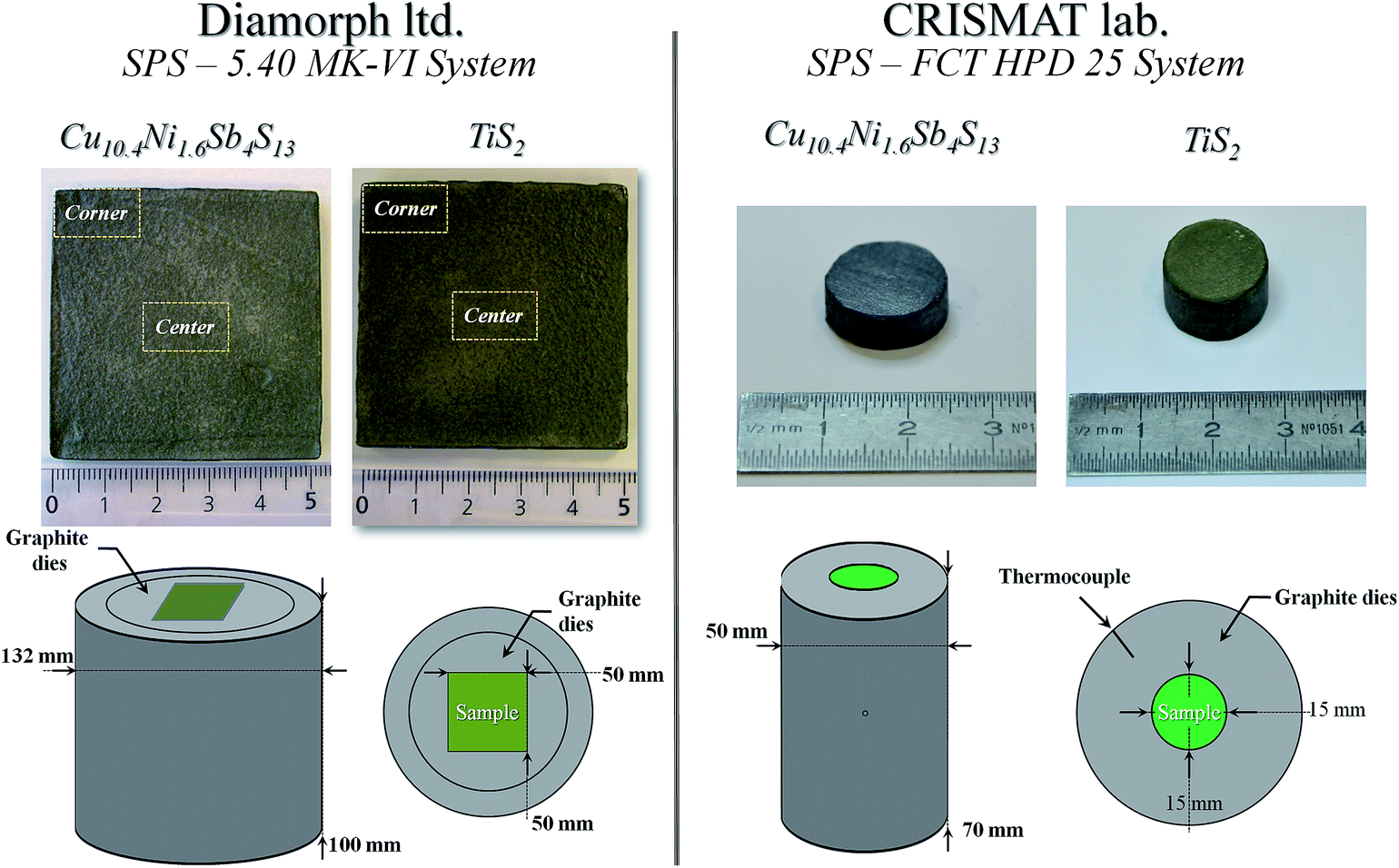 | ||
| Fig. 1 Top: TiS2 and Cu10.4Ni1.6Sb4S13 bulk specimens, sintered in SPS MK-VI Syntex (square samples) and FCT (cylindrical pellet reference samples) instruments. Bottom: Schematic representations of each of the SPS dies. | ||
The reference sample of TiS2 was sintered at 1173 K for 30 min using a heating rate of 100 K min−1 after applying a pressure of 60 MPa at room temperature. This produced 15 mm diameter pellets, ca. 9 mm thick.11 Sintering of square samples was at 1053 K, with a heating rate of 25 K min−1 from 873 K to the sintering temperature, under a pressure of 60 MPa applied at room temperature. The resulting 50 × 50 mm2 samples have a thickness of 3 mm.
For the reference tetrahedrite samples, sintering under a pressure of 60 MPa applied at room temperature, was carried out at temperatures of 673, 693 and 793 K with a holding time of 40 min and a heating rate of 50 K min−1. The fabricated 15 mm diameter pellets are of 5 mm thickness. The square sample of tetrahedrite was sintered at ca. 523 K under a pressure of 60 MPa applied at room temperature, using a holding time of 30 min and heating rate of 50 K min−1. The 50 × 50 mm2 samples are of 3 mm thickness.
Structural and microstructural properties
The crystalline phases were identified by X-Ray Diffraction (XRD) using a PANalytical X'pert Pro diffractometer (Cu Kα1–Kα2 radiations). Measurements were carried out on the surface perpendicular to the applied SPS uniaxial pressure. Data were collected over the angular range 5 ≤ 2θ/° ≤ 99 with a step size of 0.0131°, and a step time of 250 s, using a rotating sample-holder in order to increase accuracy of the measurements. The full-profile-fitting refinements were performed using the Rietveld method through the FullProf and WinPlotr software packages.21,22 The shape of the diffraction peaks was modelled using a Thompson-Cox-Hastings pseudo-Voigt profile function.23 Zero-point shift and asymmetry parameters were systematically refined, and the background contribution was estimated manually. Lattice parameters, fractional atomic coordinates and isotropic displacement parameters (i.e. Debye–Waller factors: Biso) were finally varied in order to refine the crystal structure.Microstructural observations were performed by Scanning Electron Microscopy (SEM-ZEISS Supra 55) coupled to Electron Dispersive Spectroscopy (EDS, EDAX) on breaking surfaces coming from densified samples.
Thermoelectric properties
The electrical resistivity (ρ) and Seebeck coefficient (S) of ingots cut from the sintered samples, were measured simultaneously in the temperature range 300 ≤ T/K ≤ 700, using an ULVAC-ZEM3 device, under partial helium pressure. The thermal diffusivity was analysed over the same temperature range using a Netzsch LFA-457 laser-flash instrument. The thermal conductivity (κ) was determined as the product of the geometrical density; the thermal diffusivity and the theoretical heat capacity, deduced using the Dulong–Petit approximation. In order to check any inhomogeneity in the large square samples, property measurements were performed on different regions of the samples (i.e. centre and corner, Fig. 1). Owing to the preferential orientation of the TiS2 lamellar structure, S, ρ and κ measurements were all measured along the plane perpendicular to the SPS pressure direction. Hall-effect experiments were carried out at 300 K using a Physical Properties Measurement System (PPMS Quantum Design) in a magnetic field up to 7 T.Mechanical properties
Mechanical properties were investigated by nanoindentation measurements. Superficial hardness profiles were obtained with a MTS XP nanoindentation device using the continuous stiffness measurement mode (basic hardness, modulus and tip call) allowing the measure of the hardness all along the test with a frequency of 45 Hz. Samples were slowly indented using a low loading level of a few hundreds of mN, with a constant penetration depth of 2 μm. Experiments were performed at room temperature with a diamond Berkovich tip and 20 indents were performed on each sample.Nanohardness was measured using the Oliver and Pharr methodology.24 This method is useful for brittle materials like SPS sintered thermoelectric materials, as evidenced by previous works on metallic glasses and alumina.25,26 The hardness of the material is given by:
β is a constant that depends only on geometry of the indenter and is equal to 1.034 for a Berkovich tip. F is the force and δ the displacement. The elastic modulus of the test material E may then be calculated using the following expression:

ν is the Poisson's ratio for the test material (a value of 0.21 is generally used for brittle ceramics) and Ei and νi are the elastic modulus and Poisson's ratio, respectively, of the indenter. For diamond, the elastic constants Ei = 1141 GPa and νi = 0.07 are used. Elastic modulus values are measured during the unloading with the slope at maximum loading and are averaged from 20 measurements.

Vickers micro-hardness (under a mass of 200 g for the tetrahedrite samples and 25 g for TiS2 samples) was also measured and mean measurements of 10 tests were obtained. This gives information of the bulk properties, in comparison with the more local and surface results obtained by nanoindentation.
Results and discussion
Sintering processes
Both n-type (TiS2) and p-type (Cu10.4Ni1.6Sb4S13) thermoelectric materials were sintered with two different types of pulsed electric current sintering units. The instruments differ from each other in the way the temperature is measured, making difficult the comparison of the recorded sintering temperatures directly. In the FCT unit (used to prepare reference samples), the temperature was measured using a thermocouple located in a hole at the middle of the carbon die (Fig. 1), resulting in a measurement point 2–3 mm from the sample. In this configuration, the measurement point is therefore independent of the size of the die. In the MK-VI unit (used to fabricate the large square samples), the temperature was measured either by a thermocouple (tetrahedrite) or a pyrometer (TiS2). As it is located on the outside of the die, the distance from the sample (around 30 mm here) depends on the size of the die. Therefore the size of the die will affect the temperature gradient between the measurement point and the sample. Taking into account the larger distance from measurement system to sample in MK-VI device compared to FCT, we expected higher temperature differences between that measured and that of the sample in the case of the square samples compared to the pellet samples. In order to compare conditions between SPS units, we sought to estimate the temperature difference between them, using the sintering curves of the tetrahedrite samples, since the heating kinetics were the same for the samples sintered in each instrument.The temperatures at the start and end of the sintering process were compared between the SPS units. The former were estimated by the intercept method, which consists in extracting the exact temperature from the interception of the two tangents. From the average of temperatures, the temperature difference between the units was approximated to 116 ± 20 K. For the sintering temperature at the end of the sintering process, the sintering curves presented in Fig. 2 clearly demonstrate that in the reference sample, the end of the sintering is around 700 K. However, the interpretation of the sintering curve of the square sample is more difficult as the die size and amount of graphite present in the device are much larger. This results in poor current regulation, which gives rise to fluctuations in the sintering curve. A small plateau present in the sintering (and current curves, see ESI†), just before the current drops, may be interpreted as the end of the sintering and the apparent increase in shrinkage associated with the current drop. Comparison between the FCT (reference) and MK-VI (square) units at this point, leads to an estimated temperature difference of 172 ± 20 K. Plotting the temperature difference at the start and end of the sintering (Fig. 2b) provides an estimate of the evolution with temperature of the temperature difference between the two SPS units. On the basis of this estimate, three sintered samples of tetrahedrites sintered at approximately the same “real” temperature were chosen for comparison of thermoelectric and mechanical properties, namely samples sintered at 523 K (square) and 673 and 693 K (reference).
 | ||
| Fig. 2 (a) Sintering curves of reference and square tetrahedrite samples. The sintering conditions of the reference sample were: sintering temperature/time 793 K/40 min with constant pressure of 60 MPa from RT. The sintering conditions of square samples are: sintering temperature/time 523 K/30 min and 60 MPa from RT. (b) Estimation of the change in temperature difference between the two sintering units with increasing temperature. | ||
For TiS2 the temperature difference between the SPS instruments units is difficult to estimate as the temperatures were measured with different methods and there were greater differences in heating rates. The samples sintered at 1053 K (MK-VI device, square sample) and 1173 K (FCT device, reference: pellet sample) were chosen for the comparison since they exhibit comparable geometrical densities over 95% of the theoretical densities, and absolute value of the Seebeck coefficient (see Thermoelectric properties paragraph).
Structural analysis
The results of Rietveld refinements using X-ray diffraction data of TiS2 are displayed in Fig. 3, where data acquired at corner and centre positions of the square sample are compared with those of the reference sample. Refined crystallographic parameters and reliability factors obtained are presented in Table 1. All patterns are consistent with single phase TiS2, as evidenced by the good agreement between observed and calculated data. Furthermore, the high purity of these samples is supported by the values of the RBragg factor (Table 1). The closely refined crystallographic parameters deduced from the Rietveld analysis (Table 1), and that, whatever the sintering device used or localisation of the sample extracted from bulk (a = 3.404(1) Å and c = 5.699(1) Å, a = 3.405(1) Å and c = 5.699(1) Å, a = 3.407(1) Å and c = 5.702(1) Å for the centre, corner and reference samples, respectively), suggest that these three samples are rather similar and that a good structural homogeneity occurs inside the square sample. However TiS2 square samples evidence larger preferential orientation than the reference sample. In particular, the (001) peak intensities of the corner and centre acquisitions indicate that the square sample is more textured than the reference sample; the ratio of normalized peak intensity (001)/(101) being 0.3 for square samples and 0.2 for the reference. The higher (001) texture strength in square samples may be explained by the larger shape factor (ratio surface/height) in the square samples compared to the reference, which favours the sliding and alignment of plate-like grains during SPS treatment. This behaviour is consistent with the texture development in forged samples where the material is allowed to slide within the mould during hot pressing, increasing the texture of as-produced samples.27–29 The microstructures of reference and square TiS2 samples (corner & centre) were carefully examined by scanning electron microscopy. However, due to the relatively small differences in crystallographic texture between the reference and square samples, no clear distinction could be made from a texture or grain size point of view. In addition, the absence of heterogeneities in the centre and corner parts of the sample confirms the high degree of homogeneity of the samples. EDS measurements were carried out at different locations on the pellet surface and along the cross-section of each sample. All compositions measured confirmed the nominal compositions within the measurement uncertainty. | ||
| Fig. 3 Rietveld refinements of XRD data for TiS2 collected on square (top and middle) and reference (bottom) samples. | ||
![[3 with combining macron]](https://www.rsc.org/images/entities/char_0033_0304.gif) m1 (no. 156), atomic positions: Ti on 1a (0, 0, 0); S on 2d (1/3, 2/3, z)
m1 (no. 156), atomic positions: Ti on 1a (0, 0, 0); S on 2d (1/3, 2/3, z)
| Sample | Square centre | Square corner | Reference | |
|---|---|---|---|---|
| a/Å | 3.404(1) | 3.405(1) | 3.407(1) | |
| c/Å | 5.699(1) | 5.699(1) | 5.702(1) | |
| Ti | Biso/Å2 | 1.40(1) | 1.56(1) | 1.70(1) |
| S | z | 0.246(1) | 0.247(1) | 0.247(1) |
| Biso/Å2 | 0.72(1) | 0.78(1) | 0.66(1) | |
| RBragg factor/% | 6.05 | 6.19 | 5.72 | |
| Relative geometrical density/% | 98.1 | 98.8 | 97.8 | |
The crystallographic parameters deduced by the Rietveld modelling (Table 1) show good agreement between the three TiS2 samples. Unit cell parameters for the centre, corner and reference samples respectively, are also in excellent agreement with previously reported values.6,30,31 Both structural and microstructural features confirm the high degree of homogeneity of the TiS2 square sample and demonstrate the feasibility to up-scale the sintering process to large pieces whilst maintaining high purity and good crystallinity.
Powder X-ray diffraction data of tetrahedrite-like Cu10.4Ni1.6Sb4S13, acquired from the corner and the centre of the square sample, together with those collected for the reference pellets densified at 673 and 693 K (Fig. 4) show sharp diffraction peaks corresponding to the tetrahedrite phase, characteristic of well-crystallized single phase materials. Rietveld analysis demonstrates that the data are well described by the structural model for tetrahedrite.32 Refined crystallographic parameters are presented in Table 2. Moreover, in contrast with the behaviour of TiS2, there is no preferred orientation owing to the isotropic cubic crystal structure of Cu10.4Ni1.6Sb4S13 (space group: I![[4 with combining macron]](https://www.rsc.org/images/entities/char_0034_0304.gif) 3m). As for TiS2, no microstructural and composition changes were observed on different locations of the samples.
3m). As for TiS2, no microstructural and composition changes were observed on different locations of the samples.
 | ||
| Fig. 4 Rietveld refinements of XRD patterns of Cu10.4Ni1.6Sb4S13 acquired for square (left) and reference (right) samples. | ||
3m (no. 217), atomic positions: Cu/Ni(1) on 12d site (1/4, 1/2½, 0) with fixed site occupation factor (SOF) SOF(Cu) = 0.73 and SOF(Ni) = 0.26; Cu(2) on 24g site (x, 0, 0); Sb(1) on 8c site (x, x, x), S(1) on 2a site (0, 0, 0), S(2) on 24g site (x, x, z)
| Sample | Square centre | Square corner | Reference 673 K | Reference 693 K | |
|---|---|---|---|---|---|
| a/Å | 10.316(1) | 10.319(1) | 10.318(1) | 10.321(1) | |
| Cu(1)/Ni(1) | Biso/Å2 | 1.06(1) | 1.42(1) | 1.22(1) | 1.11(1) |
| Cu(2) | x | 0.214(1) | 0.214(1) | 0.215(1) | 0.215(1) |
| Biso/Å2 | 3.61(1) | 3.78(1) | 3.77(1) | 3.63(1) | |
| Sb(1) | x | 0.268(1) | 0.268(1) | 0.268(1) | 0.268(1) |
| Biso/Å2 | 1.45(1) | 1.46(1) | 1.48(1) | 1.58(1) | |
| S(1) | Biso/Å2 | 2.87(1) | 2.86(1) | 2.95(1) | 3.10(1) |
| S(2) | x | 0.115(1) | 0.116(1) | 0.114(1) | 0.114(1) |
| z | 0.362(1) | 0.361(1) | 0.362(1) | 0.363(1) | |
| Biso/Å2 | 1.40(1) | 1.26(1) | 0.96(1) | 1.03(1) | |
| RBragg factor/% | 6.87 | 7.74 | 6.72 | 6.29 | |
| Relative geometrical density/% | 98.6 | 97.9 | 98.3 | 98.3 | |
Thermoelectric properties
Thermoelectric properties from 300 to 700 K of TiS2 ingots cut from the centre and corner regions of square specimens, as well as the reference sample, are displayed in Fig. 5. Temperature dependence in the range of 300–700 K of electrical resistivity, Seebeck coefficient and thermal conductivity of the reference sample are similar to those usually obtained for TiS2 powders sintered in graphite dies between 1073 K and 1173 K for 30 min.11,12 For both ingots from the square sample, the electrical resistivity increases linearly with temperature from 1.4 mΩ cm (RT) to around 6 mΩ cm (700 K). Such metallic temperature dependence is generally observed for TiS2 and the magnitude of the electrical resistivity is in reasonable agreement with previous studies.11,12 The Seebeck coefficient of ca. −160 to 170 μV K−1 suggests a stoichiometry of Ti1.015S2.33 The absolute value of the Seebeck coefficient is slightly higher than that of the reference sample (−140 to 150 μV K−1), which corresponds to a stoichiometry of Ti1.020S2. This suggests that the use of large graphite dies may help reduce sulphur volatilization. The temperature dependencies of the electrical resistivity and Seebeck coefficient of the two samples (centre/corner) are also similar which provides further support for the compositional homogeneity (Ti/S ratio) in addition to that of the microstructure. The small magnitude of the change of Seebeck coefficient suggests that the loss of sulphur in the edge zone of the square die is negligible. Since the electrical transport properties of TiS2 show a high sensitivity to temperature and sulphur volatilization, it suggests that the die geometry with large walls provides good temperature homogeneity and confinement. At high temperature, the electrical resistivity tends towards lower values in the square samples, in agreement with their higher (001) texture strength observed in the XRD pattern. The power factor (Fig. 5c) at 300 K is relatively high, reaching 2.0 mW m−1 K−2, decreasing to 1.1 mW m−1 K−2 at 700 K. To the best of our knowledge, such a high value at 300 K has not previously been reported for TiS2 in thin film and polycrystalline bulk forms. This suggests the measured carrier concentration of 0.4 × 1021 cm−3 is close to the optimum value to achieve the best electrical performance in TiS2 compounds. The values found for the carrier concentration and Seebeck coefficient are also in good agreement with Ti1.015S2 composition,33 for which the highest power factor was obtained in the Ti1+xS2 series. | ||
| Fig. 5 Temperature dependence of (a) electrical resistivity and Seebeck coefficient, (b) thermal conductivity, (c) PF and ZT of TiS2 reference and square samples. | ||
The thermal conductivity of square samples of TiS2 (Fig. 5b), decreases with temperature from around 4.3 W m−1 K−1 at RT to 2.5 W m−1 K−1 at 700 K. These values are higher than those measured in the reference sample, in agreement with the stronger (001) texture observed in the square sample. However, the magnitude and temperature dependence of material from both the centre and corner of the square sample of TiS2 are similar, confirming the homogeneous nature of the samples. The final ZT values are comparable between the three samples, reaching 0.35 at 700 K, demonstrating that up-scaling of the fabrication process produces TiS2 materials with comparable thermoelectric performance to that of laboratory processed samples.
Thermoelectric properties of ingots of the p-type phase, Cu10.4Ni1.6Sb4S13, cut from the centre and corner area of square specimen are displayed in Fig. 6, together with those for the reference samples. The Seebeck coefficient (Fig. 6a) shows similar values for all samples, and increases with temperature, from 120 μV K−1 at RT to 170–180 μV K−1 at 700 K. The magnitude and temperature dependence are in good agreement with those observed for similar compositions, such as Cu10.5Zn1.5Sb4S13 and Cu10.5Ni1.5Sb4S13.4,5 The magnitude of the electrical resistivity is similar for all samples, with minima of the bell curves ranging between 2.9 and 3.3 mΩ cm around 550 K (Fig. 6a). The electrical resistivity of the reference samples is slightly lower than that of the square samples.
 | ||
| Fig. 6 Temperature dependence of (a) electrical resistivity and Seebeck coefficient, (b) thermal conductivity, (c) PF and ZT of Cu10.4Ni1.6Sb4S13 reference and square samples. | ||
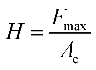
Since the geometrical densities and Seebeck coefficient are identical for all samples, we have studied the microstructures on fractured cross-sections. Scanning electron micrographs of reference and square samples of Cu10.4Ni1.6Sb4S13 (Fig. 7) reveal significant differences between the reference and square samples, with estimated average grain sizes of around 200 nm and 100 nm respectively. A lower sintering temperature in the square samples may account for the smaller grain size. This may also indicate that the estimated temperature difference of 172 K between FCT (reference) and MK-VI (square) SPS units with their respective die configurations is overestimated and is likely to be 150 K or less. Nevertheless, the high relative geometrical density obtained in the square sample (98%) is indicative of a fast densification during sintering, which probably rapidly occurs at the end of the heating ramp. This leads to very fine and dense microstructures in these tetrahedrite compounds. Microstructural differences may contribute to the slightly higher power factors in the reference samples (∼1 mW m−1 K−2 at 700 K) when compared to the square samples (∼0.85 mW m−1 K−2 at 700 K).
 | ||
| Fig. 7 SEM micrographs of (top) reference sample sintered at 693 K and (bottom) square sample sintered at 523 K (estimated 700 K). | ||
The thermal conductivity (κ), obtained using the theoretical heat capacity (Dulong–Petit law Cp = 0.44 J g−1 K−1), increases continuously with temperature and exhibits values in the range 0.8–1.0 W m−1 K−1 at 550 K (Fig. 6). In common with the Seebeck coefficient, the magnitude and temperature dependence of the thermal conductivity are comparable with those reported for Cu10.5Zn1.5Sb4S13 and Cu10.5Ni1.5Sb4S13.4,5 The slightly higher thermal conductivity of the reference samples is likely to be associated with a larger charge-carrier contribution, consistent with the lower values of electrical resistivity arising from the increased grain sizes in the reference samples. However, ZT values are closely comparable between the three samples, increasing from 0.1 at RT to 0.75 at 700 K. The similar electrical and thermal properties obtained in the centre and corner parts of the square samples confirm the high homogeneity of the present sample and provide further support for the effectiveness of the up-scaling process.
Hardness measurements
Table 3 summarises the mechanical properties determined by Vicker's microhardness and nanoindentation tests. Tetrahedrite exhibits a higher microhardness than TiS2, by a factor two on average. Moreover, reference and square samples display the same hardness despite a slightly higher dispersion obtained on square specimens. Both samples are homogeneous from the centre to the edge in terms of Vicker's hardness, showing a good reproducibility of the SPS synthesis independently of the geometry, as well as good homogeneity in square samples.| Sample | Measurement | Reference | Square |
|---|---|---|---|
| Tetrahedrite | Vickers microhardness | 291(3) | 302(19) |
| Hardness from nanoindentation (GPa) | 3.6(1) | 3.6(3) | |
| Elastic modulus from nanoindentation (GPa) | 56(1) | 53(2) | |
| TiS2 | Vickers microhardness | 113(7) | 124(25) |
| Hardness from nanoindentation (GPa) | 1.2(2) | 0.9(2) | |
| Elastic modulus from nanoindentation (GPa) | 43(4) | 43(5) |
Complementary local information on mechanical properties is given by the nanoindentation experiments. Fig. 8 shows typical load–penetration depth curves obtained from tetrahedrite and TiS2 compounds, in square and reference samples. Tetrahedrite again appears to be harder than TiS2, 3.6 GPa against 1.2 GPa (Table 3), in good agreement with the Vicker's measurements. A greater dispersion of the load–penetration curve is observed for tetrahedrite than for TiS2. The initial geometry of the samples weakly influences the hardness values in this case. However, both geometries (square and reference) have analogous mechanical properties at the surface and in the core of the samples. Hardness and elastic modulus measurements on tetrahedrites are also in good agreement with recent published data.34
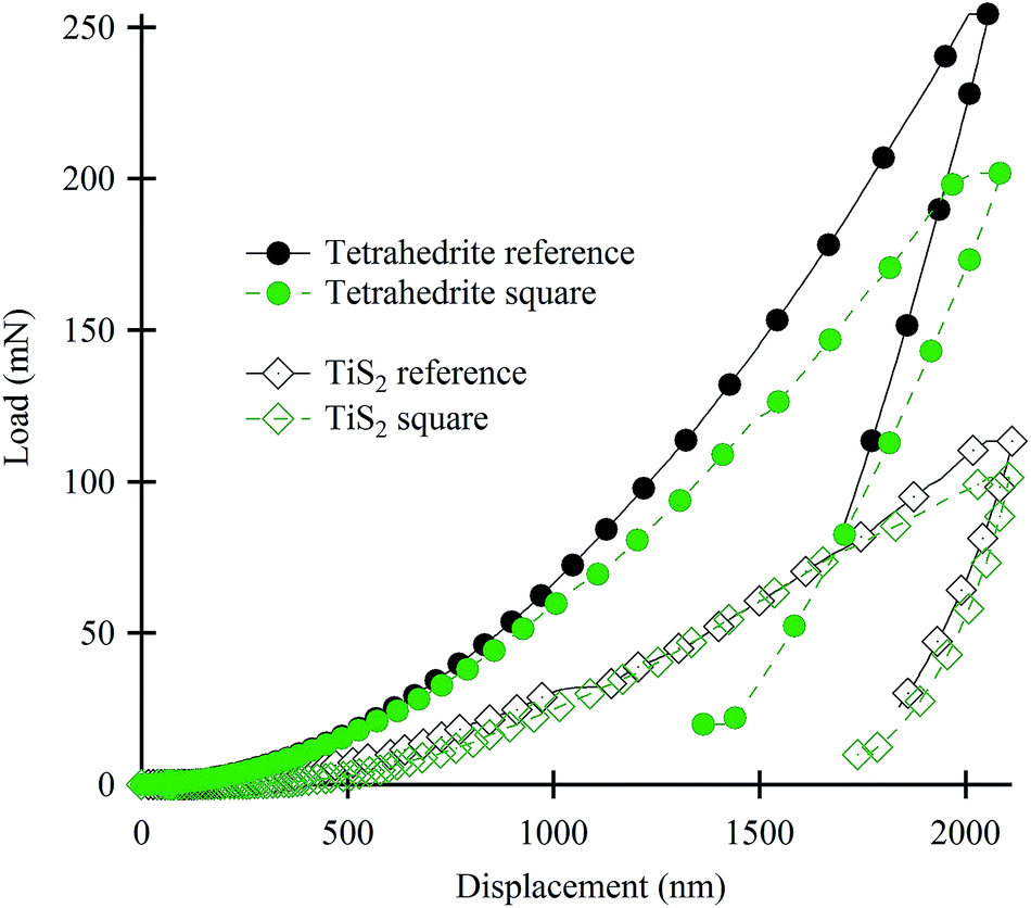 | ||
| Fig. 8 Example of load–displacement curves obtained on tetrahedrite and TiS2 samples showing the influence of the geometry of the samples. | ||
Our results clearly show that tetrahedrite compounds exhibit higher hardness value than TiS2, coupled with a better elastic rigidity. When the hardness is measured by means of Vicker's indentation, the representative volume element of the material located under the indent is sufficiently large to capture mean values that are representative of the mechanical properties of the compounds. Nanoindentation tests are directly linked to the sub-surface local mechanical properties, the maximal depth of indentation being 2 μm in our experiments.
Conclusion
Spark plasma sintering (SPS) is a versatile processing technique that enables the direct manufacture of large amounts of consolidated material. In the present study, we have successfully demonstrated that large square specimens (50 × 50 × 3 mm3) of TiS2 and tetrahedrite Cu10.4Ni1.6Sb4S13 may be fabricated by SPS. Thanks to temperature control and appropriate sample confinement in large SPS dies, the resulting monoliths are shown to be highly homogeneous, phase-pure compacts with high densities. The thermoelectric properties of the large squares of consolidated material are comparable to those of reference samples fabricated on the laboratory scale, with measured ZT values at 700 K that approach 0.75 and 0.35 for Cu10.4Ni1.6Sb4S13 and TiS2, respectively. Whilst the microstructural properties of TiS2 appear to be independent of the consolidation method, scanning electron micrographs of Cu10.4Ni1.6Sb4S13 (Fig. 7) reveal appreciably smaller grain sizes in the large square samples. The measured mechanical properties demonstrate that SPS processing of large square samples results in products in which both the sample density and microstructure are homogeneous. The scaled-up SPS results in approximately five times the volume of thermoelectric material produced by laboratory scale processing. Moreover, the square specimen geometry is optimised for the manufacture of thermoelectric legs of square cross section and may afford a cost-effective solution for consolidation of thermoelectric materials for large-scale applications.Acknowledgements
Financial support by the European Commission (FP7-SME-2012-1, Grant Agreement No. 315019) is gratefully acknowledged.References
- K. F. Hsu, S. Loo, F. Guo, W. Chen, J. S. Dyck, C. Uher, T. Hogan, E. K. Polychroniadis and M. G. Kanatzidis, Science, 2004, 303, 818–821 CrossRef CAS PubMed.
- P. F. P. Poudeu, J. D'Angelo, A. D. Downey, J. L. Short, T. P. Hogan and M. G. Kanatzidis, Angew. Chem., Int. Ed., 2006, 45, 3835–3839 CrossRef CAS PubMed.
- S. N. Girard, J. He, X. Zhou, D. P. Shoemaker, C. M. Jaworski, C. Uher, V. P. Dravid, J. P. Heremans and M. G. Kanatzidis, J. Am. Chem. Soc., 2011, 16588–16597 CrossRef CAS PubMed.
- X. Lu, D. T. Morelli, Y. Xia, F. Zhou, V. Ozolins, H. Chi, X. Zhou and C. Uher, Adv. Energy Mater., 2013, 3, 342–348 CrossRef CAS.
- K. Suekuni, K. Tsuruta, M. Kunii, H. Nishiate, E. Nishibori, S. Maki, M. Ohta, A. Yamamoto and M. Koyano, J. Appl. Phys., 2013, 113, 043712 CrossRef.
- E. Guilmeau, A. Maignan, C. Wan and K. Koumoto, Phys. Chem. Chem. Phys., 2015, 17, 24541–24555 RSC.
- P. Jood and M. Ohta, Materials, 2015, 8, 1124–1149 CrossRef.
- T. Barbier, P. Lemoine, S. Gascoin, O. I. Lebedev, A. Kaltzoglou, P. Vaqueiro, A. V. Powell, R. I. Smith and E. Guilmeau, J. Alloys Compd., 2015, 634, 253–262 CrossRef CAS.
- X. Lu and D. Morelli, J. Electron. Mater., 2014, 43, 1983–1987 CrossRef CAS.
- C. Wan, Y. Wang, N. Wang, W. Norimatsu, M. Kusunoki and K. Koumoto, J. Electron. Mater., 2011, 40, 1271–1280 CrossRef CAS.
- E. Guilmeau, Y. Bréard and A. Maignan, Appl. Phys. Lett., 2011, 99, 2–4 CrossRef.
- T. Barbier, O. I. Lebedev, V. Roddatis, Y. Bréard, A. Maignan and E. Guilmeau, Dalton Trans., 2015, 44, 7887–7895 RSC.
- X. Lu and D. T. Morelli, Phys. Chem. Chem. Phys., 2013, 15, 5762–5766 RSC.
- X. Lu and D. T. Morelli, MRS Commun., 2013, 3, 129–133 CrossRef CAS.
- T. Barbier, S. Rollin-Martinet, P. Lemoine, F. Gascoin, A. Kaltzoglou, P. Vaqueiro, A. V. Powell and E. Guilmeau, J. Am. Ceram. Soc., 2016, 99, 51–56 CrossRef CAS.
- C. Bourgès, T. Barbier, G. Guelou, P. Vaqueiro, A. V. Powell, O. I. Lebedev, N. Barrier, Y. Kinemuchi and E. Guilmeau, J. Eur. Ceram. Soc., 2016, 36, 1183–1189 CrossRef.
- O. Guillon, J. Gonzalez-Julian, B. Dargatz, T. Kessel, G. Schierning, J. Räthel and M. Herrmann, Adv. Eng. Mater., 2014, 16, 830–849 CrossRef CAS.
- M. Tokita, Blucher Material Science Proceedings, No. 1, 2014, vol. 1, pp. 3–6 Search PubMed.
- U. Anselmi-Tamburini, S. Gennari, J. E. Garay and Z. A. Munir, Mater. Sci. Eng., A, 2005, 394, 139–148 CrossRef.
- G. Molénat, L. Durand, J. Galy and a. Couret, J. Metall., 2010, 2010, 1–9 CrossRef.
- J. Rodríguez-Carvajal, Phys. B, 1993, 192, 55–69 CrossRef.
- T. Roisnel and J. Rodríguez-Carvajal, Mater. Sci. Forum, 2001, 378, 118 CrossRef.
- P. Thompson, D. E. Cox and J. B. Hastings, J. Appl. Crystallogr., 1987, 20, 79–83 CrossRef CAS.
- W. C. Oliver and G. M. Pharr, J. Mater. Res., 1992, 7, 1564–1583 CrossRef CAS.
- U. Ramamurty, S. Jana, Y. Kawamura and K. Chattopadhyay, Acta Mater., 2005, 53, 705–717 CrossRef CAS.
- D. Pravarthana, D. Chateigner, L. Lutterotti, M. Lacotte, S. Marinel, P. A. Dubos, I. Hervas, E. Hug, P. A. Salvador and W. Prellier, J. Appl. Phys., 2013, 113, 153510 CrossRef.
- J. G. Noudem, J. Eur. Ceram. Soc., 2009, 29, 2659–2663 CrossRef CAS.
- E. Guilmeau, D. Chateigner and J. G. Noudem, Supercond. Sci. Technol., 2002, 15, 1436–1444 CrossRef CAS.
- E. Guilmeau, D. Chateigner, J. Noudem, R. Funahashi, S. Horii and B. Ouladdiaf, J. Appl. Crystallogr., 2005, 38, 199–210 CrossRef CAS.
- C. Riekel and R. Schöllhorn, Mater. Res. Bull., 1975, 10, 629–633 CrossRef CAS.
- M. Beaumale, T. Barbier, Y. Bréard, S. Hébert, Y. Kinemuchi and E. Guilmeau, J. Appl. Phys., 2014, 115, 043704 CrossRef.
- B. J. Wuensch, Zeitschrift für Kristallographie, 1964, 119, 437–453 CrossRef CAS.
- M. Beaumale, T. Barbier, Y. Bréard, G. Guélou, A. V. Powell, P. Vaqueiro and E. Guilmeau, Acta Mater., 2014, 78, 86–92 CrossRef CAS.
- R. Chetty, A. Bali, M. H. Naik, G. Rogl, P. Rogl, M. Jain, S. Suwas and R. C. Mallik, Acta Mater., 2015, 100, 266–274 CrossRef CAS.
Footnote |
| † Electronic supplementary information (ESI) available. See DOI: 10.1039/c5ra23218j |
| This journal is © The Royal Society of Chemistry 2016 |