
Structural, optical and photoelectrical properties of Cu2O films electrodeposited at different pH
Chang Wanga,
Jianping Xu*a,
Shaobo Shib,
Yuzhu Zhanga,
Zeming Liua,
Xuguang Zhanga,
Shougen Yina and
Lan Li*a
aInstitute of Material Physics, Key Laboratory of Display Materials and Photoelectric Devices, Ministry of Education, Tianjin Key Laboratory for Photoelectric Materials and Devices, Tianjin University of Technology, Tianjin 300384, China. E-mail: xjp0335@163.com; Lilan@tjut.edu.cn; Fax: +86 22 60215226; Tel: +86 22 60215338
bSchool of Science, Tianjin University of Technology and Education, Tianjin 300222, China
First published on 22nd December 2015
Abstract
Cu2O films were electrodeposited on FTO and ZnO thin film substrates under different electrolyte pH. The Cu2O films on FTO substrates have a preferred orientation along the (111) planes for the match between the growing Cu2O film and the FTO substrate at the interface, whereas a transition of the preferred orientation from (100) to (111) occurs for the films on ZnO thin film substrates as electrolyte pH increases. All the Cu2O films show very similar photoluminescence (PL) spectra characteristics with a green emission band, which is related to the inter-band transitions, and a red broad emission band, which is assigned to the defects. The relative weak PL spectra for the films on ZnO thin film substrates can be ascribed to the energy and charge transfer from Cu2O to ZnO. Under light illumination, the Cu2O films on ZnO thin film substrates show the photovoltaic effect, which indicates the formation of Cu2O/ZnO heterojunctions. The photoresponse of the heterojunctions at zero bias voltage shows high sensitivity to visible light illumination, with excellent stability and reproducibility. The photocurrent is larger for the heterojunctions of the Cu2O film deposited at the pH 10.5, which is attributed to the good crystalline quality of the Cu2O film and strong built-in electric field of the ZnO/Cu2O interface.
1. Introduction
Cuprous oxide (Cu2O) is a typical p-type semiconductor with a direct band gap of 1.9–2.5 eV, and it is nontoxic, inexpensive and abundantly found in nature.1–3 Cu2O is considered to be a promising material for solar energy conversion, sensors, transistors, catalysis, nonlinear optical devices, photocathodes for H2 production and electrodes for lithium batteries because of its suitable band gap, high absorption coefficient in the visible region, high mobility, and large diffusion length of minority carriers.3–6 It is well known that morphology, crystalline quality and phase structure influence the photoelectrical properties of Cu2O films and thus the performance of Cu2O based devices.5 For example, Cu2O shows degradation properties related to its morphologies.7,8 The different exposed crystal planes of Cu2O exhibit different catalyzed reactions due to the difference in atomic arrangement, lattice symmetry and spacing.5,7 The defect states can affect the luminescence and electrical properties of Cu2O thin films.9 The absorption coefficient and charge carrier transport are closely related to the crystalline quality of Cu2O films, which determines the energy conversion efficiency of Cu2O based solar cells.5,10,11 Therefore, it is important to control the morphology and crystalline quality of Cu2O films for wide applications in electronics, photoelectronics, photocatalysis and energy conversion.Cu2O films are deposited via various methods such as thermal oxidation, chemical vapor deposition, electrodeposition, spray pyrolysis, chemical oxidation, anodic oxidation and sputtering.4 Among the different deposition methods, electrodeposition is a simple and low cost technique to deposit Cu2O films with controlled thickness.4,12 In the electrodeposition process, the deposition conditions, such as electrolyte pH and composition, deposition time and temperature, deposition current density or voltage and substrates, can affect the morphology and crystalline quality of Cu2O films. For example, the density of Cu ions vacancies can be adjusted by changing the ratio of Cu2+/OH− in the electrolyte, which then influences the optical and electric properties of Cu2O thin films.9,13 The electrolyte pH value and substrate can determine the preferential crystallographic growth orientation in the deposition process and thus the optical properties of Cu2O films.14 In this study, Cu2O films were fabricated on FTO and ZnO thin film substrates via electrodeposition using an electrolyte with different pH values. Moreover, the morphology, crystalline structure and optical-electronic properties of the Cu2O films are investigated.
2. Experimental
2.1 Preparation of ZnO nanocrystalline films
ZnO thin films were spin coated on FTO/glass substrates via sol–gel method. In a typical procedure, 0.025 mol zinc acetate dihydrate (Zn(CH3COO)2·2H2O) and 1.5 mL monoethanolamine were mixed in 50 mL 2-methoxy ethanol under stirring at 70 °C. The solution was stirred for 3 h as the precursor. All substrates were cleaned using an ultrasonic bath with detergent and deionized water, acetone, isopropanol and alcohol for 10 min. The films were spin coated at 700 rpm for 9 s and then 3000 rpm for 20 s. The ZnO thin film substrates were heated in air at 400 °C for 30 min. This coating process was repeated three times.2.2 Fabrication of Cu2O films
Cu2O films were deposited on FTO and ZnO thin film substrates using the three-electrode electrochemical method. The FTO and ZnO thin film substrates were used as the working electrodes, Pt as the counter electrode and an Ag/AgCl electrode as the reference electrode. 22.4 mL lactic acid was added to 0.625 M Cu2SO4 aqueous solution as the electrolyte. The pH of the solution was adjusted to 9.5, 10.5 and 12.5 by adding different amounts of 5 M NaOH solution. Cu2O films were deposited in the electrolyte with different pH values at 60 °C for 360 s. The depositing current density was 2 mA cm−2. The deposited Cu2O films appeared reddish brown in colour and exhibited a transparent, uniform, and smooth surface. Finally, gold (Au) electrodes (about 0.04 cm2 illuminated area) were sputtered onto the Cu2O films to form an ohmic contact.2.3 Material and device characterization
The morphologies of the Cu2O films were observed via field emission scanning electron microscopy (FESEM, Hitachi S-8010). The thickness of approximately 150 nm for the ZnO thin films and approximately 1.6 μm for the Cu2O films was obtained from surface profilometry (AlphaStep D-100). The phase and crystalline quality of the films were analyzed via X-ray diffraction (XRD, Rigaku 2500/PC) using a Cu Kα radiation source. Absorption spectra in the range of 300–800 nm were obtained on a UV-Vis spectrophotometer (Hitachi U-4100). Photoluminescence (PL) spectra were obtained on a spectrometer (FluoroLog 3, Horiba Jobin Yvon) using 450 W Xe lamp. Information on the Fermi-level of the Cu2O films was obtained from Kelvin probe force microscopy (KP020). The photovoltaic characteristics of the devices were evaluated using a Keithley 2400 Source Meter with a solar simulator equipped with an AM 1.5G filter. The photoresponse was measured at zero bias under 450 nm monochromatic light with 2.5 mW cm−2 intensity provided by the fluorescence spectrophotometer. All measurements were performed at room temperature.3. Results and discussion
The morphologies of Cu2O films deposited on FTO and ZnO thin film substrates under different pH conditions are shown in Fig. 1. The SEM images show that Cu2O films are formed in a faceted shape. For the FTO substrates, the particle size of the films increases with an increase in electrolyte pH under the same deposition current density. The Cu2O film deposited at the electrolyte pH 9.5 shows that small particles are coalesced to large particles and the film surface is uneven. With the increase in pH value, the particles become large. The crystallite shape is three-sided pyramid for the films deposited at the electrolyte pH 10.5 and four-sided pyramid for the films deposited at the electrolyte pH 12.5. For the ZnO thin film substrates, the distribution of particle size improved, as revealed from the SEM images (Fig. 1(d)–(f)). The Cu2O film deposited on the ZnO thin film substrate shows an octahedral surface morphology for the electrolyte pH 9.5 and three-sided pyramid surface for the high electrolyte pH value. The improved distribution of particle size of the Cu2O films on the ZnO thin film substrates is mainly due to the fact that FTO glass is much more conductive than ZnO, which results in the electrodeposition on the conductive substrate being faster than the growth out of the substrate.13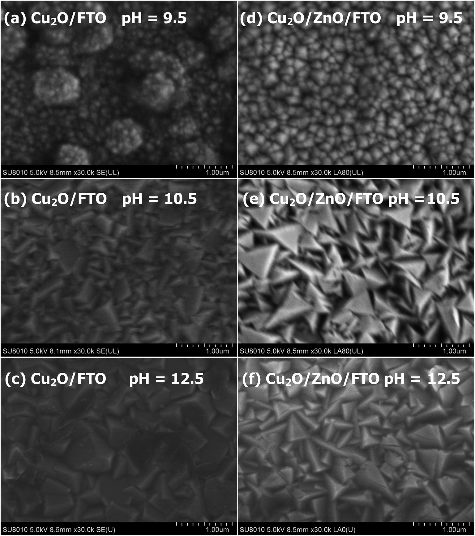 | ||
| Fig. 1 SEM images of Cu2O films with different pH values deposited on FTO (a)–(c) and ZnO thin film substrates (d)–(f). | ||
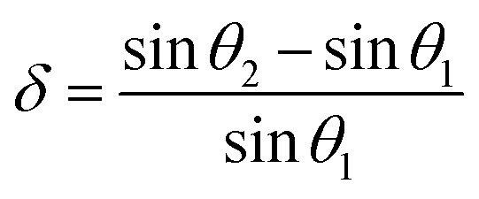
The XRD patterns of the Cu2O films prepared on FTO and ZnO thin film substrates under the different pH conditions are shown in Fig. 2(a) and (b). All the diffraction peaks can be identified as cubic Cu2O (PDF no. 050663) except for the diffraction peaks marked with an asterisk, which are from the FTO substrate. No other phase, such as Cu or CuO, was detected in the XRD patterns. The Cu2O films are polycrystalline with a preferred orientation along the (100) or (111) planes. For the FTO substrates, a dominant diffraction peak of (111) appears for all the samples and the intensity first increases and then decreases with the electrolyte pH increases from 9.5 to 12.5, whereas a transition of the preferred orientation from (100) to (111) occurs for the films on ZnO thin film substrates as the electrolyte pH increases from 9.5 to 10.5 and 12.5. A strong (111) dominant diffraction peak was observed in the Cu2O films deposited on both substrates at a pH 10.5, which indicates the good crystalline quality of the films deposited in the specific environmental conditions. The XRD results reveal that the substrate and electrolyte pH are the main factors that regulate the growth of a preferential crystallographic direction in the deposition process. Similar results have also been reported.14 For the FTO and ZnO thin film substrates, the matching between the growing Cu2O film and the substrate at the interface is different according to the equation as follows:
 | (1) |
 | ||
| Fig. 2 XRD patterns of Cu2O films deposited on FTO (a) and ZnO thin film substrates (b). | ||
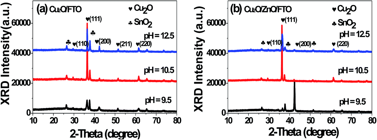
Fig. 3 shows the PL spectra for the Cu2O films deposited on FTO and ZnO substrates under different pH conditions, which were excited at 370 nm. No emission bands in the PL spectra were observed in the ZnO monolayer films under the same excitation energy, which indicate that the emission bands in the PL spectra originate from the Cu2O films. All the PL spectra present very similar characteristics: one green emission band centered at ∼520 nm and a red broad band located at ∼630 nm. The green emission is associated with inter-band transitions, whereas the red emission band is attributed to defects such as oxygen vacancies in the Cu2O films.16 Abundant defects can be generated in Cu2O films prepared via the electrodepositing method. The peaks of the emission bands have no obvious change, whereas the relative intensity of the two emission bands is different for the films deposited in different pH conditions. The relative intensity, Igreen/Ired, exhibits nonlinear increase–decrease dependence on electrolyte pH, which first increases and then decreases. It reaches a maximum under pH 10.5, which suggests the good crystalline quality of the films deposited at pH 10.5, and this is in agreement with the XRD patterns. Compared to that of the Cu2O films on FTO substrates, the PL spectra are relatively weak for the films deposited on ZnO thin film substrates in the same deposition conditions, which could be ascribed to the energy and charge transfer from Cu2O to ZnO due to the type II band alignment of ZnO/Cu2O.12
 | ||
| Fig. 3 PL spectra of Cu2O films deposited on FTO (a) and ZnO thin film substrates (b) under 370 nm excitation. | ||
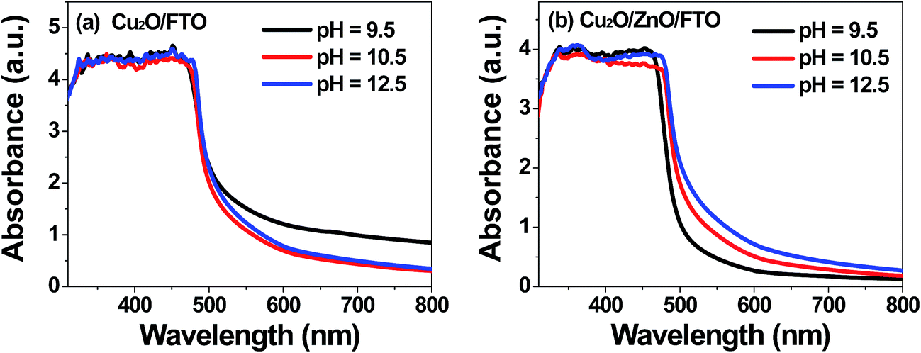
The UV-visible absorption spectra of all the Cu2O films are shown in Fig. 4(a) and (b). All the films exhibit a broad strong absorption in the UV and visible range without any discrete features. The lack of sharpness in the optical absorption feature is due to the “direct forbidden gap” nature of Cu2O.17 For the FTO substrates, the absorption edge has no obvious change and the weak visible absorption in the range of 500–800 nm first decreases and then increases with a pH change from 9.5 to 12.5. However, the absorption edge is red shifted and the visible absorption enhances with a pH increase for the Cu2O films on ZnO thin film substrates. In general, ZnO has strong absorption in the ultraviolet region of the spectrum because of its wide band-gap. It is believed that this spectral discrepancy is mainly ascribed to its different crystalline qualities and surface morphologies.12,18 The SEM images reveal that the film on FTO with pH 9.5 and the film on ZnO thin film substrate with pH 12.5 possess a rough surface and a less uniform size distribution of grains. Therefore, the visible absorption can be ascribed to the rough surface and/or defects in the Cu2O films. Band-gap narrowing is generally related to the grain size, stress/strain and impurities/defects in films.10 The large grain size of all the films does not induce the quantum confinement effect. The calculated lattice constant of the films deposited on ZnO thin film substrates, which was obtained from XRD patterns, is 4.26120 Å, 4.27242 Å and 4.2693 Å for cubic Cu2O films with pH 9.5, 10.5 and 12.5, respectively. The similar trend of the lattice constant is consistent with the optical band gap of Cu2O films with different pH. Stress/strain could be the main reason for the band-gap narrowing.
 | ||
| Fig. 4 UV-Vis absorption spectra of Cu2O films on FTO (a) and ZnO thin film substrates (b). | ||
To study the photoelectric properties of the films, Au electrodes were sputtered onto the Cu2O films and devices with an FTO/Cu2O/Au and FTO/ZnO/Cu2O/Au structure were obtained. The I–V characteristics of the devices in the dark state are shown in Fig. 5(a). The I–V curves of all the FTO/Cu2O/Au devices in dark and light conditions are similar and the typical curves of the device with the Cu2O film deposited at pH 10.5 are shown in the inset of Fig. 5(a). The linear characteristics of the FTO/Cu2O/Au devices reveal ohmic-type contacts between Au and Cu2O and between FTO and Cu2O. Under the light condition, the current has an obvious increase, which is a typical photoconductive property of semiconductors. Electron–hole pairs are generated in the Cu2O film when the photon energy becomes larger than the band-gap of the semiconductor. The non-linear I–V curves of the FTO/ZnO/Cu2O/Au devices exhibit a similar rectifying characteristic. This rectification behavior mainly arises from the Cu2O/ZnO contact. The calculated rectifying ratio of the devices is very low in general, but the rectifying ratio of the device with the Cu2O film deposited at pH 10.5 is much better than that of the other devices. The relatively large forward current with small leakage current for this device could be related to the good crystallization quality of the Cu2O film at pH 10.5.
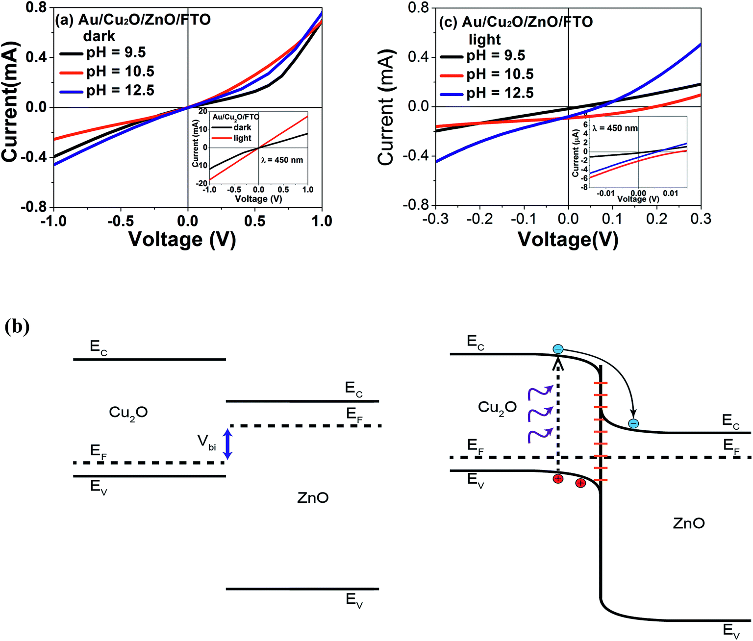 | ||
| Fig. 5 I–V curves of the Au/Cu2O/ZnO/FTO device under dark condition (a). Inset of (a) shows the I–V curves of the Au/Cu2O/FTO device under dark and light illumination. Band alignment for bare ZnO, Cu2O and Cu2O/ZnO structures (b). I–V curves of Au/Cu2O/ZnO/FTO device under AM 1.5 solar simulator illumination (c). Inset of (c) shows the I–V curve of Au/Cu2O/ZnO/FTO devices under 450 nm light illumination. | ||
Although the thickness of the ZnO film is thin and its diffraction peaks were not detected by XRD, its rectification behavior indicates the formation of a heterojunction between Cu2O and ZnO. Cu2O is a well known p-type material and ZnO is an n-type wide band-gap semiconductor. Their bands have a good type-II band alignment, as shown in Fig. 5(b). The Fermi level obtained from the Kelvin probe force is −5.21 eV, −5.33 eV and −5.24 eV for Cu2O films deposited at pH 9.5, 10.5 and 12.5, respectively. The Fermi level of the Cu2O film first shifts to the top of the valence band and then moves as the pH increases from 9.5 to 12.5. The ZnO thin films on FTO substrates can be considered the same as these three devices due to the same fabrication conditions. The Cu2O film deposited at pH 10.5 generates a larger Fermi level difference (namely a stronger interfacial electric field, Vbi) after the construction of the heterostructure with ZnO. For the ZnO/Cu2O heterostructure, the magnitude of the interfacial field, Vbi, dominates the separation efficiency of the photogenerated carriers in Cu2O. A larger Vbi means a greater amount of photogenerated carrier separation in ZnO/Cu2O, which is beneficial to the photoresponse.12
The photovoltaic effects in the ZnO/Cu2O heterojunctions were investigated under AM 1.5 and 450 nm monochromatic light. Fig. 5(c) shows the J–V curves of the FTO/ZnO/Cu2O/Au devices. A small but measurable photovoltaic effect was observed under the illumination. The maximum conversion efficiency value is 0.17% for the device with Cu2O film deposited at pH 10.5. This result indicates the FTO/ZnO/Cu2O/Au device can be used as a self-powered photodetector without any external energy supply for the photovoltaic effect. The Cu2O films have strong absorption in the blue light region, as observed from their absorption spectra (Fig. 3). The photocurrent response properties and stability of the FTO/ZnO/Cu2O/Au device were investigated at a nominal zero set bias under the on/off switching radiation of blue light (λ = 450 nm), as shown in Fig. 6(a) and (b). Four cycles of switching the blue light on and off demonstrated the good stability and reproducibility of the photoresponse. The steep rise and fall edges suggest the fast photoresponse of the devices. The devices display similar blue-light sensitive behaviors except for a small photocurrent difference between the three devices under the same measurement conditions. The photocurrent had a slight increasing trend during the illumination, which is attributed to the generation of the carriers in the quasi-neutral region.19 The photocurrent is larger for the device with the Cu2O film deposited at pH 10.5. Under the illumination of blue light, the photon energy is below the ZnO band gap and these photons are absorbed on the Cu2O films and then produce electron–hole pairs. The proper built-in electric field that arises from the well-aligned energy-band structure (see Fig. 5(b)) of the device can efficiently separate the photogenerated electron–hole pairs in the Cu2O film at the ZnO/Cu2O interface and help the charge carrier transport to the corresponding electrodes, which result in a photocurrent. The rise time and decay time is generally defined as the time required for the photocurrent to increase from 10% to 90% and decrease from 90% to 10%, respectively.20 For the FTO/ZnO/Cu2O/Au device with the Cu2O film deposited at pH 10.5, the rise time and decay time is 65 ms and 46 ms, respectively, which are calculated from the enlarged rising and decaying edges of the photocurrent response, as shown in Fig. 6(b), indicating a relatively fast photocurrent response behavior. The good crystalline quality of the Cu2O film deposited at pH 10.5 and strong built-in electric field of the ZnO/Cu2O interface are the main causes for the fast photoresponse. The responsivity is an important parameter for photodetectors, which can be defined as follows:
 | (2) |
 | ||
| Fig. 6 Photoresponse measurements of Au/Cu2O/ZnO/FTO devices at zero bias under 450 nm light illumination. I–t curves (a) and magnified view of the rise and fall in photocurrent during light switch on and off (b). | ||
4. Conclusion
In summary, Cu2O films were fabricated on FTO and ZnO thin film substrates at different electrolyte pH via the electrodepositing method. The substrates and electrolyte pH value can influence the morphologies, crystalline structure, and optical and photoelectrical properties of the Cu2O films. The Cu2O films deposited at pH 10.5 have a good crystalline quality and their Fermi level is close to the top of the valence band. The Cu2O films on ZnO thin film substrates show the photovoltaic effect and photoresponse without any external energy supply. The excellent stability and reproducibility of the fast photoresponse under visible light indicate that the Cu2O/ZnO structure is suitable as a self-powered photodetector.Acknowledgements
This study was supported by the National High Technology Research and Development Program of China (863 Program) (Grant No. 2013AA014201), the Natural Science Foundation of Tianjin (Grant No. 14JCZDJC31200, 15JCYBJC16700 and 15JCYBJC16800), the National Key Foundation for Exploring Scientific Instrument of China (Grant No. 2014YQ120351) and the International Cooperation Program from Science and Technology of Tianjin (Grant No. 14RCGHGX00872).References
- T. Kazimierczuk, D. Fröhlich, S. Scheel, H. Stolz and M. Bayer, Giant Rydberg excitons in the copper oxide Cu2O, Nature, 2014, 514, 343–347 CrossRef CAS PubMed.
- C. L. Li, Y. B. Li and J. J. Delaunay, A novel method to synthesize highly photoactive Cu2O microcrystalline films for use in photoelectrochemical cells, ACS Appl. Mater. Interfaces, 2014, 6, 480–486 CAS.
- L. B. Xiong, S. Huang, X. Yang, M. Q. Qiu, Z. H. Chen and Y. Yu, P-type and n-type Cu2O semiconductor thin films: controllable preparation by simple solvothermal method and photoelectrochemical properties, Electrochim. Acta, 2011, 56, 2735–2739 CrossRef CAS.
- S. Bijani, L. Martınez, M. Gabás, E. A. Dalchiele and J. R. Ramos-Barrado, Low-temperature electrodeposition of Cu2O thin films: Modulation of micro-nanostructure by modifying the applied potential and electrolytic bath pH, J. Phys. Chem. C, 2009, 113, 19482–19487 CAS.
- S. D. Sun, Recent advances in hybrid Cu2O-based heterogeneous nanostructures, Nanoscale, 2015, 7, 10850–11088 RSC.
- Y. T. Xu, Y. Guo, C. Li, X. Y. Zhou, M. C. Tucker, X. Z. Fu, R. Sun and C. P. Wong, Graphene oxide nano-sheet wrapped Cu2O microspheres as improved performance anode materials for lithium ion batteries, Nano Energy, 2015, 11, 38–47 CrossRef CAS.
- B. J. Heng, T. Xiao, X. Y. Hua, M. Yuan, W. Tao, W. Huang and Y. W. Tang, Catalytic activity of Cu2O micro-particles with different morphologies in the thermal decomposition of ammonium perchlorate, Thermochim. Acta, 2011, 524, 135–139 CrossRef CAS PubMed.
- X. L. Deng, Q. Zhang, E. Zhou, C. J. Ji, J. Z. Huang, M. H. Shao, M. Ding and X. J. Xu, Morphology transformation of Cu2O sub-microstructures by Sn doping for enhanced photocatalytic properties, J. Alloys Compd., 2015, 649, 1124–1129 CrossRef CAS.
- A. Chowdhurya, P. K. Bijalwana and R. K. Sahu, Investigations on the role of alkali to obtain modulated defect concentrations for Cu2O thin films, Appl. Surf. Sci., 2014, 289, 430–436 CrossRef.
- K. Cheng, Q. Q. Li, J. Meng, X. Han, Y. Q. Wu, S. J. Wang, L. Qian and Z. L. Du, Interface engineering for efficient charge collection in Cu2O/ZnO heterojunction solar cells with ordered ZnO cavity-like nanopatterns, Sol. Energy Mater. Sol. Cells, 2013, 116, 120–125 CrossRef CAS.
- S. J. Chen, L. M. Lin, J. Y. Liu, P. W. Lv, X. P. Wu, W. F. Zheng, Y. Qu and F. C. Lai, An electrochemical constructed p-Cu2O/n-ZnO heterojunction for solar Cell, J. Alloys Compd., 2015, 644, 378–382 CrossRef CAS.
- S. T. Ren, G. H. Fan, M. L. Liang, Q. Wang and G. L. Zhao, Electrodeposition of hierarchical ZnO/Cu2O nanorod films for highly efficient visible light-driven photocatalytic applications, J. Appl. Phys., 2014, 115, 064301 CrossRef.
- L. C. Wang, N. R. de Tacconi, C. R. Chenthamarakshan, K. Rajeshwar and M. Tao, Electrodeposited copper oxide films: Effect of bath pH on grain orientation and orientation-dependent interfacial behavior, Thin Solid Films, 2007, 515, 3090–3095 CrossRef CAS.
- I. S. Brandt, C. A. Martins, V. C. Zoldan, A. D. C. Viegas, J. H. D. Silva and A. A. Pasa, Structural and optical properties of Cu2O crystalline electrodeposited films, Thin Solid Films, 2014, 562, 144–151 CrossRef CAS.
- C. L. Jiao, S. R. Zhao, X. Q. Qiang and Y. F. Wei, The relationship of lattice mismatch the HgCdTe/CdZnTe with X-ray diffraction, Laser Infrared, 2007, 37, 910–914 CAS.
- J. W. Park, H. K. Jang, S. Kim, S. H. Choi, H. Lee, J. Kang and S. H. Wei, Microstructure, optical property, and electronic band structure of cuprous oxide thin films, J. Appl. Phys., 2011, 110, 103503 CrossRef.
- Y. L. Pan, S. Z. Deng, L. Polavarapu, N. Y. Gao, P. Y. Yuan, C. H. Sow and Q. H. Xu, Plasmon-enhanced photocatalytic properties of Cu2O nanowire–Au nanoparticle assemblies, Langmuir, 2012, 28, 12304–12310 CrossRef CAS PubMed.
- W. L. Yu, Y. Z. Lin, X. W. Zhu, Z. G. Hu, M. J. Han, S. S. Cai, L. L. Chen and H. H. Shao, Diversity of electronic transitions and photoluminescence properties of p-type cuprous oxide films: A temperature-dependent spectral transmittance study, J. Appl. Phys., 2015, 117, 045701 CrossRef.
- J. P. Clifford, G. Konstantatos, K. W. Johnston, S. Hoogland, L. Levina and E. H. Sargent, Fast, sensitive and spectrally tuneable colloidal quantum-dot photodetectors, Nat. Nanotechnol., 2009, 4, 40–44 CrossRef CAS PubMed.
- Q. H. Li, L. Wei, Y. R. Xie, K. Zhang, L. Liu, D. P. Zhu, J. Jiao, Y. X. Chen, S. S. Yan, G. L. Liu and L. M. Mei, ZnO nanoneedle/H2O solid-liquid heterojunction based self-powered ultraviolet detector, Nanoscale Res. Lett., 2013, 8, 415 CrossRef PubMed.
- Y. W. Shen, X. Q. Yan, Z. M. Bai, X. Zheng, Y. H. Sun, Y. C. Liu, P. Lin, X. Chen and Y. Zhang, A self-powered ultraviolet photodetector based on solution-processed p-NiO/n-ZnO nanorod arrayheterojunction, RSC Adv., 2015, 5, 5976–5981 RSC.
| This journal is © The Royal Society of Chemistry 2016 |