
Realization of a flexible and mechanically robust Ag mesh transparent electrode and its application in a PDLC device†
Liangfei Qiab,
Jia Li*a,
Chaoting Zhua,
Ye Yanga,
Shijin Zhaob and
Weijie Song*a
aNingbo Institute of Material Technology and Engineering, Chinese Academy of Sciences, Ningbo, 315201, P. R. China. E-mail: lijia@nimte.ac.cn; Fax: +86-574-87913375; Tel: +86-574-87913375
bInstitute of Materials Science, Shanghai University, Shanghai, 200072, P. R. China
First published on 26th January 2016
Abstract
In this paper, flexible Ag electrodes with a hexagonal micromesh structure were fabricated on PET substrate using a photolithography technique. The effect of film thickness on optical and electrical properties of Ag electrodes was investigated systematically. Furthermore, these flexible transparent Ag mesh electrodes were firstly applied to a polymer dispersed liquid crystal (PDLC) device and its performance was evaluated. All of the Ag electrodes exhibited a high average transmittance of about 80.2–85.0% in the visible range (400–800 nm), and the minimum sheet resistance value reached 8.2 Ω sq−1. The prepared Ag mesh also showed an excellent performance of adhesion and bending, demonstrating its superior durability. The PDLC device based on Ag mesh electrodes showed comparable performance with that using ITO electrodes, indicating that the Ag mesh film can be a good substitution for ITO electrodes in PDLC devices and may find practical application in large area flexible devices.
1 Introduction
In recent years, flexible devices have become an emerging trend and are finding various applications in daily life.1 A polymer dispersed liquid crystal (PDLC) device, which has a basis structure of liquid crystals sandwiched by a pair of electrodes on a flexible PET substrate, is a promising device to modulate electro-optical performance in display devices and smart windows.2 Most commonly, the transparent conducting electrodes (TCEs) used for flexible devices nowadays are still based on a transparent conductive oxide, particularly indium-tin oxide (ITO) due to its excellent optical transmittance and low sheet resistance in the visible range of the electromagnetic spectrum.3 However, an ITO electrode has drawbacks such as high price due to In metal deficiency and brittleness due to its ceramic nature, which restrain its application in large-scale flexible devices.4 In recent decades, alternative TCEs have been investigated to replace ITO, including carbon nanotube networks,5,6 graphene,7 conductive polymers,8,9 random nanowires10,11 and Ag mesh.12–14 Among these, Ag mesh electrodes are promising candidates because they offer good optical transparency and high electrical conductivity as well as superior mechanical stability.15 It has been demonstrated theoretically and experimentally that their optical and electrical properties could be tuned relatively independently by changing the relevant geometrical parameters of Ag mesh structures, such as line width (w), period (p), and thickness (h).12,16,17Generally, the network structure of Ag mesh electrodes can be designed to be random or regular in shape. Random Ag mesh electrodes were fabricated by some novel methods such as nanosphere lithography,18 electrospun nanotroughs,19 inject printing,20,21 laser sintering,22 and methods based on the coffee ring effect.23,24 Recently, random Au meshes fabricated by grain lithography have demonstrated 83% transmittance at 20 Ω sq−1.25 Ag networks on PET are prepared by depositing Ag film inside the gaps of a cracked TiO2 gel mold, which has a high transmittance of 88% at 10 Ω sq−1.26 Ag gratings of 78% transmittance at 23 Ω sq−1 have been investigated using nanoimprint lithography.27 However, these methods could give rise to problems of complex treatments and nonuniform performances which rely on the repeatability of molding.
On the other hand, physical lithography methods such as electron beam lithography, nanoimprint and photolithography have been used to prepare uniform and ordered Ag meshes, which is in favor of the repeatability and device stability thanks to its uniform structure. However, the two previous methods are relatively costly and not scalable. As a conventional technique, photolithography has been applied for large-area patterning.28 Ag mesh electrodes fabricated using a photolithography method show a transmittance of 74% at about 7 Ω sq−1.29,30 While these electrodes are mostly prepared on rigid substrates, few works are about flexible substrates. Furthermore, to our knowledge, the fabrication of a PDLC device with a Ag mesh film acting as electrodes has not been reported.
In this work, we demonstrate a hexagonal Ag mesh on PET substrates directly by photolithography, which act as the electrodes for the PDLC device. The effects of film thickness on their performance are investigated systematically. The optical, electrical and mechanical properties of this Ag mesh film as well as the performance of the PDLC device are evaluated in detail.
2 Experimental
2.1 Fabrication procedure
Polyethylene terephthalate (PET) substrates were sequentially cleaned in ethanol, acetone and deionized water by ultrasonication for 2 minutes each, followed by drying with nitrogen gas. Photolithography was performed in a yellow room inside a cleanroom. Fig. 1 shows the schematic diagram of the fabrication of the Ag mesh film. A KMP e3130b photoresist (Kempur Microelectronics, China) was first spin coated on the PET substrates at 3500 rpm for 35 seconds and prebaked at 90 °C for 90 seconds. After exposing to 365 nm UV light using an ABM/6/350/NUV/DCCD/M Manual Mask Aligner System (ABM, USA) for 40 seconds, the photoresist was developed in KMP PD238 developer (Kempur Microelectronics, China) for 40 seconds. Ag films of different thicknesses (10 nm, 25 nm, 40 nm, 55 nm, 70 nm) were sputtered onto the samples after 5 nm thick Cr deposition, acting as an adhesive layer, using JCP-350M2 magnetron sputtering apparatus (Technol, China). Finally, Ag mesh films were patterned after a lift-off process in acetone. The line width and periodicity were set as 4 μm and 100 μm, respectively.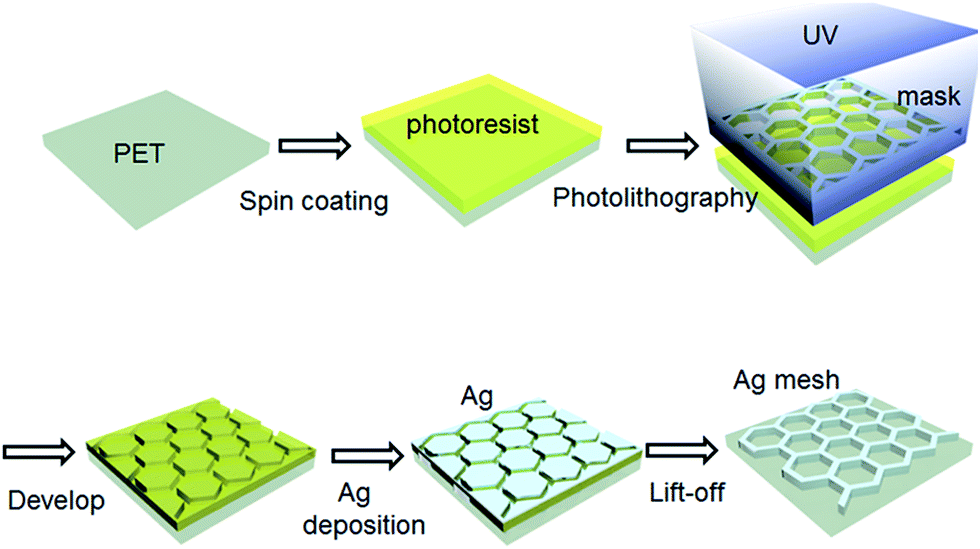 | ||
| Fig. 1 Schematic of the Ag mesh film fabrication process. | ||
A PDLC device was fabricated using the above prepared Ag mesh as a transparent electrode. NOA 65 (Norland products) and nematic LC E7 (Yantai Xianhua Chem-Tech. Co., Ltd) were used as the pre-polymer and nematic LC mixture, respectively. The mixing ratio of NOA 65 and E7 was fixed at 2![[thin space (1/6-em)]](https://www.rsc.org/images/entities/char_2009.gif) :3. Silica microspheres with a mean diameter of 60 μm were used as spacers to control the thickness of the PDLC device. The substrates, Ag mesh coated PET films were cut into 40 mm × 40 mm pieces. Before using as electrodes, a thin layer of ZnO:Al with a thickness of 50 nm was deposited on the Ag mesh for protection, ensuring the uniform conductivity of the electrode. The LC/NOA65 mixture was coated and spread on the bottom Ag mesh electrode and then covered by a top Ag mesh electrode. The sandwich structure was then exposed to UV light with the intensity of 15 mW cm−2 for 8 min.
:3. Silica microspheres with a mean diameter of 60 μm were used as spacers to control the thickness of the PDLC device. The substrates, Ag mesh coated PET films were cut into 40 mm × 40 mm pieces. Before using as electrodes, a thin layer of ZnO:Al with a thickness of 50 nm was deposited on the Ag mesh for protection, ensuring the uniform conductivity of the electrode. The LC/NOA65 mixture was coated and spread on the bottom Ag mesh electrode and then covered by a top Ag mesh electrode. The sandwich structure was then exposed to UV light with the intensity of 15 mW cm−2 for 8 min.
2.2 Characterization and measurement
The surface morphologies of the Ag mesh films were examined using a field emission scanning electron microscope (FE-SEM, Hitachi S-4800). The optical transmittance and haze of the Ag mesh films were obtained at room temperature using a UV-Vis-NIR spectrophotometer (Agilent, Cary 5000). The sheet resistance was measured using a four-point probe system (ST-2258A). The thicknesses of the films were calculated and conformed using atomic force microscopy (Veeco, Dimension 3100V). To investigate the mechanical properties, a bending test was carried out with home-made equipment. The adhesion test was performed using a 12.7 mm wide 3 M scotch tape to attach onto the Ag mesh film and then peeled off from the sample. To evaluate the performance of the fabricated PDLC device, the specular transmittance–voltage curve was measured using a spectroscopic ellipsometer (model M2000DI) with an alternating voltage potential (0–120 V) applied across the device.3 Results and discussion
3.1 Microstructure of Ag mesh films
Five hexagonal Ag mesh films with thicknesses of 10, 25, 40, 55 and 70 nm were prepared on PET substrates. Fig. 2 shows the SEM images and the optical image of the fabricated 70 nm Ag micromesh patterns on the PET substrate. Fig. 2a indicates a uniform and perfect metal network, and the enlarged image (Fig. 2b) shows that the Ag wires are well connected with a straight boundary and smooth surface. The Ag film deposited using magnetic sputtering on an amorphous PET substrate indicated good quality with compact and homogenous distribution of small particles of about 200 nm (Fig. 2c). The line width measured from Fig. 2c is about 5.5 μm, deviating from the designed value of 4 μm for the mask, which may be because of the deviation of the mask fabrication and photolithography process. The uniform and compact Ag film morphologies benefit its conductivity and mechanical performance. Fig. 2d shows the optical image of a Ag mesh film on a PET substrate, the letters on paper can be clearly seen through the Ag mesh transparent film.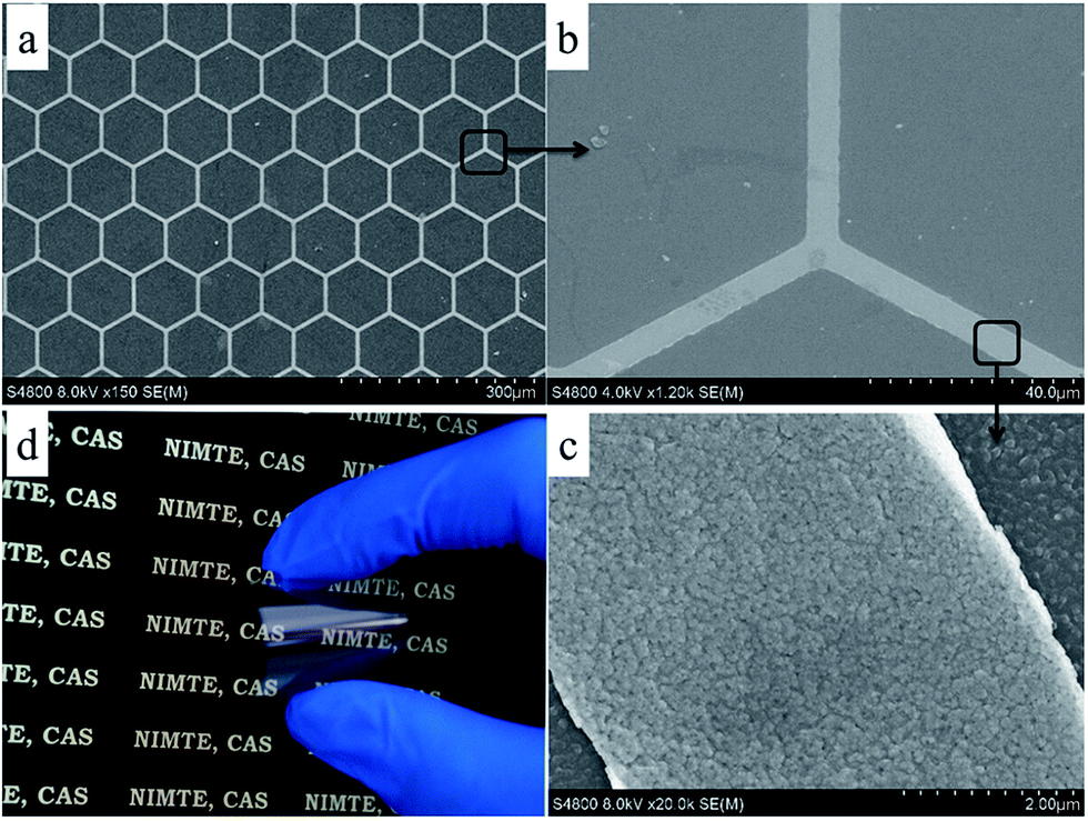 | ||
| Fig. 2 (a) SEM image of the fabricated Ag mesh on a PET substrate; (b) and (c) enlarged SEM images of Ag films; (d) optical image of the Ag mesh film on PET. | ||
3.2 Optical and electrical properties of Ag mesh films
Fig. 3 shows the optical transmittance spectra of the fabricated Ag mesh with different thicknesses, all transmittance spectral measurements were referenced to air. Ag mesh films have almost constant transmittance values in the whole wavelength range. The average transmittance of the Ag mesh films on PET with 10, 25, 40, 55, and 70 nm film thicknesses in the entire visible wavelength range (400–800 nm) were 85.0%, 82.7%, 81.5%, 81.6% and 80.2%, respectively. This indicates that all the Ag mesh films possess uniformity and a high transmittance of >80% in a broad wavelength range. It was noticed that there is a slight decline while the film thickness is increasing to 70 nm, which may be because of the lager line width. Taking the open area ratio of the Ag mesh as 92% and the transmittance of the PET substrate as 90%,31 the theoretical transmittance of the Ag mesh film should be around 82.8%. The transmittance of a Ag mesh of 10 nm film thickness in our experiment is 85%, which is attributed to the transparency of the Ag film when the thickness is less than 10 nm.32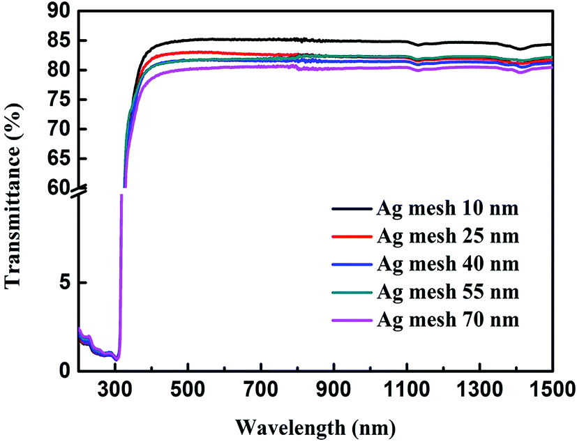 | ||
| Fig. 3 Transmittance of Ag meshes on a PET substrate with 10, 25, 40, 55, and 70 nm thicknesses. | ||
Sheet resistance values were measured and are summarized in Table 1. The measured sheet resistances of the Ag mesh films with thicknesses of 10, 25, 40, 55 and 70 nm were 108.3, 42.5, 18.1, 12.3, and 8.2 Ω sq−1, respectively, which demonstrated a significant reduction when the film thickness increased from 10 nm to 70 nm. It indicates that the sheet resistance of the transparent metal electrode could be controlled relatively independently by adjusting the thickness of the Ag mesh without sacrificing the optical transmittance, which is far different from the other types of TCEs including TCOs, CNTs, and nanowires, where there is a trade-off between optical transmittance and sheet resistance, making it a great challenge for these TCEs to obtain good optical and electrical properties simultaneously.
| Thickness (nm) | T (%) | R (Ω sq−1) | FOM | Haze (%) | |
|---|---|---|---|---|---|
| Ag mesh film | 10 | 85.0 | 108.3 | 20.5 | 1.1 |
| 25 | 82.7 | 42.5 | 44.5 | 1.7 | |
| 40 | 81.5 | 18.1 | 96.7 | 2.2 | |
| 55 | 81.6 | 12.3 | 143.2 | 2.6 | |
| 70 | 80.2 | 8.2 | 194.7 | 2.2 | |
| ITO film30 | — | 85.7 | 13.4 | 175.5 | — |
To evaluate the effect of mesh thickness on the overall performance of the TCEs, a figure of merit (FOM) was determined, which was the ratio of the electrical conductance and the optical conductance. The equation of DC/OPT is as follows:
 | (1) |
The haze values of different Ag mesh films are also measured and shown in Table 1. The haze value is defined as the ratio of diffusive transmittance to total transmittance, with illumination from the glass side. The thicker the Ag thickness, the higher the haze value. The haze value reached saturation after the Ag thickness was larger than 40 nm. Although the value was far less than that of Ag nanowires reported in literature, a low haze value not larger than 1% is important to their application, especially for touch screen applications.
3.3 Mechanical properties of Ag mesh films
Besides electrical and optical properties, mechanical stability of the TCE film on a flexible substrate is also vital for its applications. To further evaluate the mechanical stability of the Ag mesh transparent electrodes, a cyclic bending test and an adhesive tape test were performed. Fig. 4 shows the bending test. The original length of the Ag mesh on PET is L = 30 mm, the deformation of each cycle is dL = 15 mm, therefore, the bending radius is R = 6.7 mm, and strain is ε = 1.0% according to ε = h/2R (where h is the whole thickness of the Ag mesh and PET, and R is the bending radius34). The same measurement was done on ITO coated PET as a comparison. As can be seen in Fig. 4, commercial ITO’s resistance increased significantly and reached 1200.0 Ω after 2000 bending cycles. Fig. 4a shows the SEM image of the ITO film after 2000 bending cycles. Some micro cracks developed perpendicular to the bending direction, which was due to the brittleness of the ITO film. The formation of these micro cracks lead to a deteriorative electrical conductivity during repeated deformation. In contrast, the changes in resistance of Ag mesh films were far less than that of the ITO film. The mechanical performance of the Ag mesh films was influenced by the film thickness. The 10 nm Ag mesh film showed an inferior performance after bending, which may be due to the small film thickness. Increasing the film thickness demonstrated an apparent improvement of stability (showed in Fig. S2†). For the samples with a Ag thickness of 70 nm, the change in resistance was less than 5% of its original value (from 10.0 to 10.2 Ω) throughout 2000 bending cycles. The SEM image of the Ag mesh after 2000 bending cycles (Fig. 4b) also confirmed that the Ag mesh structure remained unchanged and no cracks could be observed.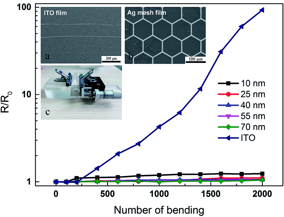 | ||
| Fig. 4 Effect of repeated bending on the sheet resistance of the ITO and Ag mesh. SEM images of ITO (a) and Ag meshes (b) after 2000 bending cycles; (c) test setup of cyclic bending. | ||
The tape test was also conducted to evaluate the adhesion between the Ag mesh film and PET substrate. Fig. 5 shows the changes in sheet resistance of Ag mesh films with different thicknesses during the repeated adhesive tape test. The adhesive properties improved with increasing Ag mesh film thickness. The inferior performance of the 10 nm sample was due to the peeling off of the mesh film from the substrate in some part because of low thickness (as shown in Fig. S3†). The changes in the resistance value decreased and kept steady for thicker films. For the sample with the 70 nm Ag film, the sheet resistance changed slightly (<5%) after 100 cycles, which is superior to Ag nanowire films.35 Both the bending test and tape test indicated that our Ag mesh electrodes demonstrate excellent flexibility and adhesion, as well as high optical and electrical properties, which may benefit their applications in optoelectronic devices.
 | ||
| Fig. 5 Changes in the sheet resistance of the Ag mesh films during the adhesive tape test. | ||
3.4 Performance of the PDLC device with Ag mesh electrodes
The PDLC device was fabricated to evaluate its performance with a Ag mesh film as the electrode. The Ag mesh film with 70 nm Ag thickness was chosen for device fabrication. A device using commercial PET/ITO film with almost the same sheet resistance value (8 Ω sq−1, brought from KDX Co., Ltd.) was prepared at the same conditions for comparison. Conductive copper tape was stuck on each electrode for better contact. Fig. 6a shows the specular transmittance–voltage curve of the PDLC devices at the wavelength of 550 nm using a Ag mesh film and an ITO film as electrodes, respectively. The device with the Ag mesh film as the electrode shows almost the same performance as that with the ITO electrode. The specular transmittance value is around zero when the voltage is below 20 V, indicating an off state of the device. A linear increase in transmittance with a steep slope between 30 V and 70 V can be observed. After that, the specular transmittance tends towards saturation with voltage increasing above 70 V. The maximum specular transmittance is 41%. In general, the driving voltage can be defined at the applied voltage of an optical transmittance of 90% of the maximum value,36 thus the driving voltage in this device is around 80 V. The thickness of the cell gap of this device is 60 μm, which leads to a higher driving voltage and lower specular transmittance compared to devices with a thinner cell gap.37 Fig. 6b and c show the photographic images of the device with Ag mesh electrodes at off and on states, respectively. An AC voltage of 100 V was selected as the on state voltage. In the off state, the device presents opaque color with good scattering properties. After applying voltage, the device became transparent with some milky color, indicating a relatively high haze value. The PDLC device with Ag mesh electrodes shows a high contrast ratio and uniformity in both on and off states. It indicates that the Ag mesh film can be a good substitute for the ITO electrode in a PDLC device and may find application in large area flexible device fabrication. | ||
| Fig. 6 (a) The specular transmittance–voltage curve of the PDLC device with a Ag mesh and an ITO electrode. Photographic images of the PDLC device with a Ag mesh electrode at (b) the off state and (c) on state. | ||
4 Conclusions
We have demonstrated a hexagonal Ag mesh transparent conductive electrode on a PET flexible substrate. The Ag mesh is patterned by photolithography with a fixed line width of 4 μm and periodicity of 100 μm. Five different Ag mesh films were prepared with thicknesses from 10 nm to 70 nm. All samples showed a high optical transmittance of >80% as well as a good conductivity of 8 Ω sq−1 at a film thickness of 70 nm. This can be used to change the optical transmittance and electrical resistance independently by adjusting the film thickness, line width and periodicity. The Ag mesh produced using photolithography and magnetic sputtering on a flexible substrate also showed an excellent stability in terms of adhesion and bending. Furthermore, this Ag mesh electrode can be a good electrode candidate for a PDLC device with a high contrast ratio and uniformity at both on and off states.Acknowledgements
This work was supported by the Natural Science Foundation of China (No. 21377063), Zhejiang Natural Science Foundation (No. LY15F040004) and the International S & T Cooperation Program of China (No. 2015DFH60240).References
- J. Z. Song and H. B. Zeng, Angew. Chem., Int. Ed., 2015, 54, 9760–9774 CrossRef CAS PubMed.
- Y. Kim, D. Jung, S. Jeong, K. Kim, W. Choi and Y. Seo, Curr. Appl. Phys., 2015, 15, 292–297 CrossRef.
- M. Layani, A. Kamyshny and S. Magdassi, Nanoscale, 2014, 6, 5581–5591 RSC.
- K. S. Kim, Y. Zhao, H. Jang, S. Y. Lee, J. M. Kim, K. S. Kim, J.-H. Ahn, P. Kim, J.-Y. Choi and B. H. Hong, Nature, 2009, 457, 706–710 CrossRef CAS PubMed.
- Z. C. Wu, Z. H. Chen, X. Du, J. M. Logan, J. Sippel, M. Nikolou, K. Kamaras, J. R. Reynolds, D. B. Tanner, A. F. Hebard and A. G. Rinzler, Science, 2004, 305, 1273–1276 CrossRef CAS PubMed.
- D. S. Hecht, A. M. Heintz, R. Lee, L. Hu, B. Moore, C. Cucksey and S. Risser, Nanotechnology, 2011, 22, 075201 CrossRef PubMed.
- J. H. Zhu, M. J. Chen, Q. L. He, L. Shao, S. Y. Wei and Z. H. Guo, RSC Adv., 2013, 3, 22790–22824 RSC.
- S.-I. Na, S.-S. Kim, J. Jo and D.-Y. Kim, Adv. Mater., 2008, 20, 4061–4067 CrossRef CAS.
- K. Ellmer, Nat. Photonics, 2012, 6, 808–816 CrossRef.
- Q. J. Huang, W. F. Shen and W. J. Song, RSC Adv., 2015, 5, 45836–45842 RSC.
- J. Z. Song, J. H. Li, J. Y. Xu and H. B. Zeng, Nano Lett., 2014, 14, 6298–6305 CrossRef CAS PubMed.
- J. van de Groep, P. Spinelli and A. Polman, Nano Lett., 2012, 12, 3138–3144 CrossRef CAS PubMed.
- N. Kwon, K. Kim, S. Sung, I. Yi and I. Chung, Nanotechnology, 2013, 24, 235205 CrossRef PubMed.
- M.-G. Kang, H. J. Park, S. H. Ahn and L. J. Guo, Sol. Energy Mater. Sol. Cells, 2010, 94, 1179–1184 CrossRef CAS.
- H.-J. Kim, S.-H. Lee, J. Lee, E.-S. Lee, J.-H. Choi, J.-H. Jung, J.-Y. Jung and D.-G. Choi, Small, 2014, 10, 3767–3774 CrossRef CAS PubMed.
- P. B. Catrysse and S. Fan, Nano Lett., 2010, 10, 2944–2949 CrossRef CAS PubMed.
- F. Afshinmanesh, A. G. Curto, K. M. Milaninia, N. F. van Hulst and M. L. Brongersma, Nano Lett., 2014, 14, 5068–5074 CrossRef CAS PubMed.
- T. C. Gao, B. M. Wang, B. Ding, J. K. Lee and P. W. Leu, Nano Lett., 2014, 14, 2105–2110 CrossRef CAS PubMed.
- H. Wu, D. Kong, Z. Ruan, P.-C. Hsu, S. Wang, Z. Yu, T. J. Carney, L. Hu, S. Fan and Y. Cui, Nat. Nanotechnol., 2013, 8, 421–425 CrossRef CAS PubMed.
- B. Y. Ahn, D. J. Lorang and J. A. Lewis, Nanoscale, 2011, 3, 2700–2702 RSC.
- Y. Li, L. Mao, Y. Gao, P. Zhang, C. Li, C. Ma, Y. Tu, Z. Cui and L. Chen, Sol. Energy Mater. Sol. Cells, 2013, 113, 85–89 CrossRef CAS.
- S. Hong, J. Yeo, G. Kim, D. Kim, H. Lee, J. Kwon, H. Lee, P. Lee and S. H. Ko, ACS Nano, 2013, 7, 5024–5031 CrossRef CAS PubMed.
- M. Layani, M. Gruchko, O. Milo, I. Balberg, D. Azulay and S. Magdassi, ACS Nano, 2009, 3, 3537–3542 CrossRef CAS PubMed.
- Z. Zhang, X. Zhang, Z. Xin, M. Deng, Y. Wen and Y. Song, Adv. Mater., 2013, 25, 6714–6718 CrossRef CAS PubMed.
- C. F. Guo, T. Sun, Q. Liu, Z. Suo and Z. Ren, Nat. Commun., 2014, 5, 3121 Search PubMed.
- B. Han, K. Pei, Y. Huang, X. Zhang, Q. Rong, Q. Lin, Y. Guo, T. Sun, C. Guo, D. Carnahan, M. Giersig, Y. Wang, J. Gao, Z. Ren and K. Kempa, Adv. Mater., 2014, 26, 873–877 CrossRef CAS PubMed.
- M.-G. Kang, M.-S. Kim, J. Kim and L. J. Guo, Adv. Mater., 2008, 20, 4408–4413 CrossRef CAS.
- S. M. Huang, L. M. Dai and A. W. H. Mau, Adv. Mater., 2002, 14, 1140–1143 CrossRef CAS.
- F. L. M. Sam, C. A. Mills, L. J. Rozanski and S. R. P. Silva, Laser Photonics Rev., 2014, 8, 172–179 CrossRef CAS.
- J. W. Lim, Y. T. Lee, R. Pandey, T. H. Yoo, B. I. Sang, B. K. Ju, K. Hwang do and W. K. Choi, Opt. Express, 2014, 22, 26891–26899 CrossRef CAS PubMed.
- K. Neyts, A. Real, M. Marescaux, S. Mladenovski and J. Beeckman, J. Appl. Phys., 2008, 103, 093113 CrossRef.
- H. Kang, S. Jung, S. Jeong, G. Kim and K. Lee, Nat. Commun., 2015, 6, 6503 CrossRef CAS PubMed.
- Y. H. Kim, C. Sachse, M. L. Machala, C. May, L. Muller-Meskamp and K. Leo, Adv. Funct. Mater., 2011, 21, 1076–1081 CrossRef CAS.
- J. L. Ni, X. F. Zhu, Z. L. Pei, J. Gong, C. Sun and G. P. Zhang, J. Phys. D: Appl. Phys., 2009, 42, 175404 CrossRef.
- Q. Huang, W. Shen, X. Fang, G. Chen, Y. Yang, J. Huang, R. Tan and W. Song, ACS Appl. Mater. Interfaces, 2015, 7, 4299–4305 CAS.
- J. Kim and J. I. Han, Electron. Mater. Lett., 2014, 10, 665–669 CrossRef CAS.
- H. H. Khaligh, K. Liew, Y. Han, N. M. Abukhdeir and I. A. Goldthorpe, Sol. Energy Mater. Sol. Cells, 2015, 132, 337–341 CrossRef.
Footnote |
| † Electronic supplementary information (ESI) available. See DOI: 10.1039/c5ra21988d |
| This journal is © The Royal Society of Chemistry 2016 |