
Hierarchical TiO2–B/anatase core/shell nanowire arrays for efficient dye-sensitized solar cells
Hong-Yan Chen*,
Jie Fan,
Hua-Shang Rao,
Hao-Lin Feng,
Wen-Guang Li,
Dai-Bin Kuang* and
Cheng-Yong Su
MOE Key Laboratory of Bioinorganic and Synthetic Chemistry, Lehn Institute of Functional Materials, School of Chemistry and Chemical Engineering, Sun Yat-sen University, Guangzhou 510275, P. R. China. E-mail: chenhy33@mail.sysu.edu.cn; kuangdb@mail.sysu.edu.cn
First published on 1st December 2015
Abstract
The fabrication of hierarchically structured photoanode materials is believed to be an effective way to obtain efficient dye-sensitized solar cells (DSSCs). In this paper, hierarchical TiO2–B/anatase core/shell heterojunction nanowire arrays on a titanium plate substrate are synthesized and used as novel photoanode materials for DSSCs. By using H2Ti3O7 nanowire arrays as the precursor template, anatase nanoparticle coated TiO2–B nanowire arrays are prepared via a hydrothermal reaction followed by a calcination process. Photoelectric measurements reveal that the anatase nanoparticle shell makes the pristine TiO2–B nanowire rougher for more dye adsorption and effective light scattering, which can enhance the light harvesting ability and thus the photocurrent density of the photoanode largely. Moreover, the dynamic electron transport and recombination study via electrochemical impedance spectroscopy (EIS) and intensity modulated photocurrent/photovoltage spectroscopy (IMPS/IMVS) measurements reveal that the TiO2–B/anatase composite photoanode based cell has a faster electron transport and higher electron collection efficiency than a TiO2–B based cell. As a consequence, the photoelectric conversion efficiency of the hierarchical composite photoanode was greatly enhanced to 4.88%, which is among the highest reported value for TiO2 nanowire array photoanodes grown on titanium plate substrate.
1. Introduction
Since the pioneering work of Grätzel and co-workers, dye-sensitized solar cells (DSSCs) have become an attractive solar energy conversion technology due to their low cost, facile fabrication process and relatively high power conversion efficiency.1,2 As the carrier for dye adsorption and the transport path for photo-generated electrons, the photoanode plays a key role in determining the photovoltaic performances of DSSC devices, and should provide a large surface area and a strong light scattering ability to ensure sufficient light harvesting, and also fast electron transport to efficiently collect electrons. Therefore, much effort has been devoted to exploring excellent photoanode materials, and a variety of semiconductor metal oxides (such as TiO2, ZnO, SnO2, ZnSnO4, etc.) with different structures and morphologies (nanoparticles, 1D and 2D nanostructures, hybrid structures, etc.) have been well studied in recent years.3–6 Given that small nanoparticle (smaller than 25 nm) based photoanodes always suffered from a weak light scattering effect and serious electron recombination resulting from their small particle size and thus a large amount of grain boundaries and defects,7–9 research on 1D and quasi-1D nanostructured materials with strong light scattering and fast electron transport ability was put on the schedule.10,11 However, the achieved conversion efficiency was not satisfactory in that the surface area of these structures were low. To address the problem, hierarchical 1D nanostructures constructed by growing nano-branches (such as nanoparticles, nanorods, nanosheets, etc.) on a pristine matrix,12–14 became a hot issue. The composite structure utilized secondary nano-building blocks to compensate for the lower surface area of the pristine nanowire, which combined with the fast electron transportation and slow electron recombination of the 1D matrix contributed to the higher power conversion efficiency.TiO2 is one of the most commonly used wide-gap semiconductors. It has four main polymorphs in nature, including anatase, rutile, brookite and TiO2–B. Among them, anatase crystal was widely used due to its excellent stability and photoelectric properties.15 TiO2–B is a metastable monoclinic morphology of TiO2 with a relatively open structure which performs well in lithium-ion batteries.16,17 Recently, TiO2–B and its mixed-phase composites with anatase were also reported to show good photocatalytic activity in the photocatalytic degradation of organic matter and water splitting.18–21 However, compared with other polymorphs, less attention was paid to TiO2–B for its application in DSSCs. Pure TiO2–B nanobelts, nanorods, and nanoparticles have been reported as photoanode materials, but the conversion efficiency was a little low, usually less than 2.5%.22,23 To improve the performance, 1D TiO2–B nanostructures were always mixed with anatase nanoparticles to integrate the large surface area of nanoparticles with the fast electron transport and light scattering effect of 1D materials.24,25 However, there still existed lots of electron transfer interfaces among nanoparticles and neighbouring 1D nanostructures which should be detrimental to electron transport and collection. In addition, it was well established that a mixed-phase structure of TiO2–B and anatase was beneficial to the photoelectrical performance of composite materials due to the energy band differences between the two phases. The principal reason is similar to P25, a kind of commercial TiO2 nanoparticle with an average size of ca. 20 nm which is composed of the anatase and rutile phases,26 whose difference between the conduction band (CB) edges can promote irreversible charge transfer from one phase to the other.27,28 This concept has been demonstrated in photocatalytic applications.19,20 Therefore, the fabrication of a hierarchical TiO2–B 1D array photoanode with a mixed-phase crystal structure may be a good choice to achieve excellent photovoltaic performance.
Herein, TiO2–B/anatase core/shell nanowire arrays on titanium plate substrate were synthesized and used as novel photoanode materials for efficient DSSCs. The synthesis process involved a hydrothermal growth of H2Ti3O7 nanowire arrays first, followed by a secondary hydrothermal process to form an anatase nanoparticle shell on the outer surface, and then a calcination process was carried out to transform the inner core to the TiO2–B phase. The light harvesting capability of this composite photoanode was investigated using a dye adsorption amount test and UV-vis diffuse reflectance spectra, and the dynamic electron transport and recombination were investigated via electrochemical impedance spectroscopy (EIS) and intensity modulated photocurrent/photovoltage spectroscopy (IMPS/IMVS) measurements. It was revealed that the hierarchical TiO2–B/anatase mixed-phase photoanode can provide a larger dye adsorption amount and a stronger light scattering effect, and also had a faster electron transport and higher electron collection efficiency than a TiO2–B photoanode. As a result, the photoelectric conversion efficiency of the TiO2–B nanowire based cell was greatly enhanced to 4.88%.
2. Experimental
2.1 Synthesis of TiO2–B nanowire arrays (BNW) and TiO2–B/anatase core/shell nanowire arrays (BANW)
BNW were synthesized through the thermal dehydration of H2Ti3O7 nanowire arrays. First, a titanium plate (2.5 × 3 cm2) was cleaned ultrasonically for 15 min with detergent, water, ethanol and acetone in turn. Then the dried plate was placed at an angle against the wall of a Teflon-lined stainless-steel autoclave containing 30 mL 1 M NaOH aqueous solution. The autoclave was sealed and put into an electronic oven, maintained at 220 °C for 24 hours, and cooled down to room temperature naturally. The obtained nanowire arrays were cleaned several times with water to remove redundant NaOH, then immersed in 0.2 M HCl solution for 15 min. This soak process was repeated 3 times to ensure that all the Na+ was replaced with H+ to form H2Ti3O7 nanowires. After washing with water, the H2Ti3O7 nanowires were dried at 70 °C for 30 min and then calcined in a muffle furnace at 400 °C for 4 h. For the preparation of BANW, the as-prepared H2Ti3O7 nanowires underwent another hydrothermal process at 110 °C for 24 h to grow an outer anatase crystal shell. The reaction solution was 30 mL of 0.05 M HNO3 aqueous solution. After thoroughly cleaning with water, the obtained samples were calcined in the muffle furnace at 450 °C for 4 h to convert the inner H2Ti3O7 core to the TiO2–B phase.2.2 Assembly of DSSCs devices
The as-prepared BNW and BANW films were treated with TiCl4 by soaking in 0.04 M TiCl4 aqueous solution at 70 °C for 30 min, and then sintered at 520 °C for 30 min. This process coated the pristine nanowires with a layer of nanoparticles to improve the interfacial connection. To distinguish it from the pristine film, the TiCl4 treated BNW film was denoted as BNW–TiCl4. All the photoanode films were immersed in N719 dye solution at a high temperature for about 20 h to adsorb dye molecules. The concentration of N719 was 0.5 mM in a mixed solvent of acetonitrile and tert-butanol (volume ratio, 1![[thin space (1/6-em)]](https://www.rsc.org/images/entities/char_2009.gif) :1). Afterward, these films were rinsed with acetonitrile and dried in air. Then the dye-sensitized photoanodes were assembled with Pt counter electrodes to form sandwich type cells with I−/I3− redox pair based liquid electrolyte sandwiched between them. The Pt counter electrodes were prepared by the thermal deposition of H2PtCl6 solution (5 mM in isopropanol) at 400 °C using an FTO glass substrate. The composition of the electrolyte was 0.03 M I2, 0.05 M LiI, 0.6 M 1-methyl-3-propylimidazolium iodide, 0.10 M guanidinium thiocyanate, and 0.5 M tert-butylpyridine dissolved in a solvent mixture of acetonitrile and valeronitrile (volume ratio, 85:15).
:1). Afterward, these films were rinsed with acetonitrile and dried in air. Then the dye-sensitized photoanodes were assembled with Pt counter electrodes to form sandwich type cells with I−/I3− redox pair based liquid electrolyte sandwiched between them. The Pt counter electrodes were prepared by the thermal deposition of H2PtCl6 solution (5 mM in isopropanol) at 400 °C using an FTO glass substrate. The composition of the electrolyte was 0.03 M I2, 0.05 M LiI, 0.6 M 1-methyl-3-propylimidazolium iodide, 0.10 M guanidinium thiocyanate, and 0.5 M tert-butylpyridine dissolved in a solvent mixture of acetonitrile and valeronitrile (volume ratio, 85:15).
2.3 Characterizations
The crystal structure and morphology of the samples were investigated using X-ray powder diffractometry (XRD, Bruker D8, Cu Kα radiation, λ = 1.5418 Å), confocal Raman Spectroscopy (Renishaw inVia), field emission scanning electron microscopy (FE-FEM, JSM-6330F) and transmission electron microscopy (TEM, JEOL-2010-HR). The diffuse reflectance ability and dye adsorption amount of photoanode films was monitored by UV-vis diffuse reflectance spectra and absorption spectra, respectively, both on a UV-vis-NIR spectrophotometer (Shimadzu, UV-3150). To determine the dye adsorption amount, the dye-sensitized photoanode films were immersed in 0.1 M NaOH aqueous solution to detach the dye molecules, and the characteristic absorbance of the dye solution at 520 nm was recorded to calculate the dye amount according to Lambert–Beer’s Law. The current density–voltage (J–V) curves of the DSSCs were recorded using a Keithley 2400 source meter under AM 1.5 G (100 mW cm−2) illumination. The light source was a solar light simulator (Oriel, 91192), whose incident light intensity was calibrated by a NREL-calibrated Si solar cell. An electrochemical workstation (Zahner, Zennium) was used to perform the electrochemical impedance spectroscopy (EIS) and intensity-modulated photocurrent/photovoltage spectroscopy (IMPS/IMVS). The EIS was measured in the dark at a bias potential of open-circuit voltage with the frequency ranging from 10 mHz to 1 MHz and an alternative signal of 10 mV. For IMPS/IMVS measurements, the incident light intensity was set at 30, 60, 90, 120 and 150 W m−2, and the scanning frequency range was set from 1000 Hz to 10 mHz.3. Result and discussion
It is well known that the thermal dehydration of H2Ti3O7 is a feasible way to prepare TiO2 polymorphs.12,19,29 By using a titanium plate as the starting material to react with NaOH under hydrothermal conditions and followed by a H+ exchange reaction process, H2Ti3O7 nanowire arrays on a titanium plate substrate were prepared first, which were converted to the TiO2–B phase subsequently via calcination at 400 °C. Fig. 1a shows the XRD patterns of the as-prepared nanowires (bottom curve). The diffraction peaks agree with the standard TiO2–B phase peaks well (JCPDS 74-1940) and no peaks corresponding to other TiO2 crystal phases can be observed, indicating that the pure phase TiO2–B nanowire arrays (denoted as BNW) have been obtained. To prepare TiO2–B/anatase core/shell nanowire arrays (denoted as BANW), a secondary hydrothermal reaction was carried out on the surface of pristine H2Ti3O7 nanowire arrays to generate an anatase crystal layer, and then the H2Ti3O7 core was converted to the TiO2–B phase via sintering. The XRD pattern (Fig. 1a, up curve) confirms the co-existence of the two crystal phases, although the characteristic peaks corresponding to anatase (JCPDS 21-1272) are very strong while the signal for TiO2–B is a little weak. This mixed-phase structure can also be demonstrated by Raman spectra, which has been verified to be a sensitive detection method to distinguish the crystal form of samples.30,31 As shown in Fig. 1b, different patterns are observed for the BNW and BANW samples. BNW exhibits typical characteristic peaks corresponding to TiO2–B, which is consistent with previous reports,31 while the BANW exhibits both the peaks of TiO2–B and anatase. Therefore, it can be inferred that pure phase TiO2–B and TiO2–B/anatase mixed-phase nanowire arrays have been successfully prepared.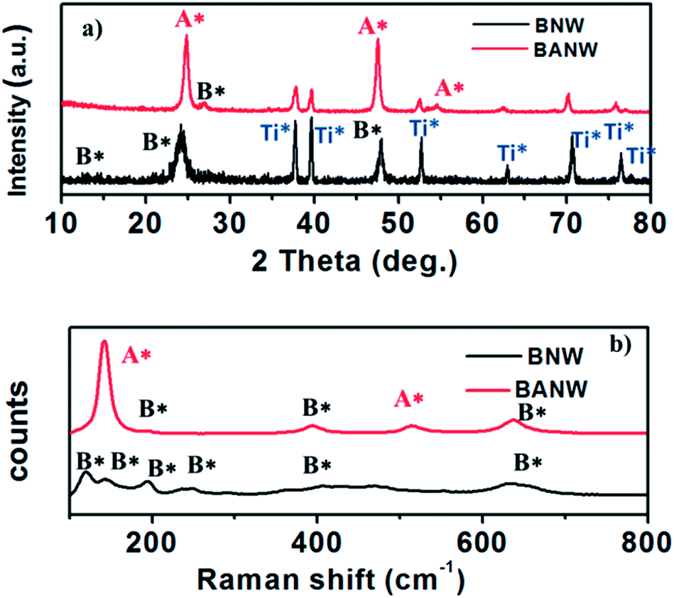 | ||
| Fig. 1 XRD (a) and Raman patterns (b) of BNW and BANW samples. | ||
The morphology and structure of the as-prepared samples were examined using field emission scanning electron microscopy (FE-FEM) and transmission electron microscopy (TEM). As shown in Fig. 2a–c, the pure phase TiO2–B nanowire arrays consist of smooth nanowires with a diameter of ∼80 nm, and the length of the nanowire array is ∼16 μm. Moreover, the HR-TEM image (Fig. 2c, inset) further confirmed that the crystal form is the TiO2–B phase. After the secondary hydrothermal growth process, anatase nanoparticles of several nanometers can be clearly observed on the surface, while the inner core remains in the TiO2–B phase (Fig. 2d–f). In addition, the diameter of a single nanowire is increased to ∼120 nm while the length of the nanowire array is reduced to ∼15 μm. These results further confirmed that TiO2–B/anatase core/shell nanowire arrays were successfully prepared.
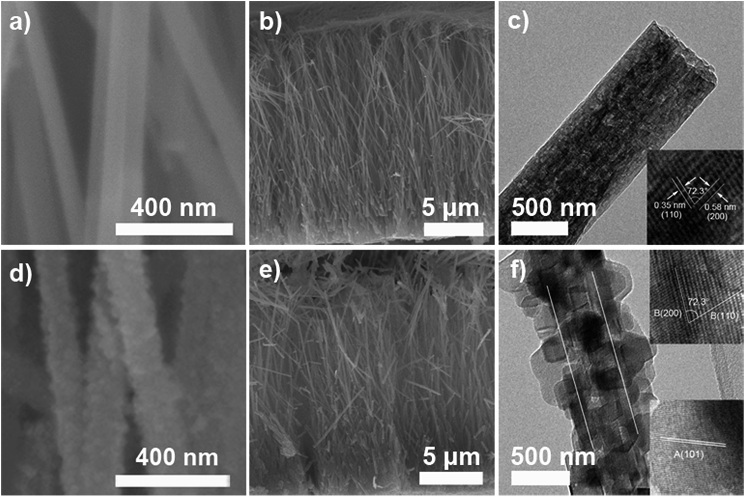 | ||
| Fig. 2 (a and b) SEM and (c) TEM images of BNW, inset in (c) is the corresponding HR-TEM image showing the TiO2–B crystal structure; (d and e) SEM and (f) TEM images of BANW, inset in (f) is the corresponding HR-TEM images showing the TiO2–B and anatase crystal structure. | ||
The low dye adsorption amount is an important factor limiting the photovoltaic performance of 1D nanostructured photoanodes. The surface area enlargement by roughening the surface of the nanowires should be an effective solution. Therefore, the as-prepared composite photoanode films were assembled into DSSC devices and tested. For comparison, three cells based on pure TiO2–B nanowire array films (BNW), TiCl4 treated TiO2–B nanowire array films (TiO2–B nanowire films coated with a thin anatase nanoparticle layer, denoted as BNW–TiCl4) and TiO2–B/anatase core/shell nanowire array films (BANW) were tested. The BNW–TiCl4 film was prepared by soaking TiO2–B nanowire arrays in TiCl4 aqueous solution, a method which is known to improve the current density of DSSCs.32–34 Different from hydrothermal treatment, the nanoparticle coating via TiCl4 treatment was very thin and partially amorphous. Fig. 3 shows the photocurrent density–voltage (J–V) curves of the three cells and the corresponding photovoltaic parameters including the short circuit current density (Jsc), open circuit voltage (Voc), overall energy conversion efficiency (η) and fill factor (FF) are listed in Table 1. The pure phase BNW cell shows a conversion efficiency of 1.22%, with Jsc of 2.28 mA cm−2, Voc of 706 mV and FF of 0.76. After treatment with the TiCl4 solution, the Jsc value of the BNW–TiCl4 cell increases greatly to 4.06 mA cm−2, and the Voc slightly increases to 718 mV while the FF decreases to 0.71, thus leading to a η of 2.08%. This value can be further improved to 4.88% when the anatase nanoparticle shell was coated on the TiO2–B nanowires via the hydrothermal process. In detail, the Jsc of the BANW cell increased further to 8.98 mA cm−2, and the Voc increased to 756 mV, while the FF increased to 0.72.
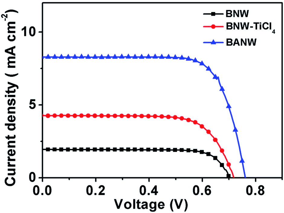 | ||
| Fig. 3 (a) Photocurrent density–photovoltage (J–V) curves of DSSCs based on the BNW, BNW–TiCl4, and BANW photoanodes. | ||
| Cell | Jsc (mA cm−2) | Voc (mV) | η (%) | FF | Dye uptake (nmole cm−2) |
|---|---|---|---|---|---|
| BNW | 2.28 | 706 | 1.22 | 0.76 | 59.14 |
| BNW–TiCl4 | 4.06 | 718 | 2.08 | 0.71 | 66.85 |
| BANW | 8.98 | 756 | 4.88 | 0.72 | 104.46 |
Obviously, both the Jsc and Voc were improved when the anatase nanoparticle coating formed on the surface of the BNW. In particular, the Jsc was increased from 2.28 to 8.98 mA cm−2 after the core/shell mixed-phase structure formation, and an over four times improvement was obtained. It is known that the Jsc value of solar cells is determined by the light-harvesting efficiency (LHE), electron injection efficiency (ηinj), and electron collection efficiency (ηcc) of the cell and the incident light intensity.35 To detect the LHE of different photoanodes, the dye anchoring amount and light scattering ability were examined. According to UV-Vis absorption spectra measurement, the dye amount anchored on the BANW photoanode was calculated to be 104.46 nmol cm−2, which was much larger than BNW (59.14 nmol cm−2) and BNW–TiCl4 (66.85 nmol cm−2). It means that the nanoparticle decoration can enhance the surface area greatly thus providing more active sites for dye adsorption. Undoubtedly, the larger amount of dye molecules can absorb more photons to generate electrons. On the other hand, the light scattering effect of the photoanodes was examined using diffuse reflection spectra. As shown in Fig. 4, the TiCl4 treated sample shows a slightly higher diffuse reflection than BNW since a very thin nanoparticle layer was coated on the bare nanowires. Surprisingly, the BANW sample shows much higher reflection over the whole visible light region, especially in the range from 400 nm to 600 nm. This phenomenon can be attributed to the scattering effect of the outer anatase nanoparticle shell which makes the nanowire surface much rougher and individual nanoparticles can also act as light-scattering centres, especially in the short wavelength range.36 The large dye anchoring amount and strong light scattering ability of the BANW composite photoanode should lead to a high LHE and thus a largely enhanced Jsc value.
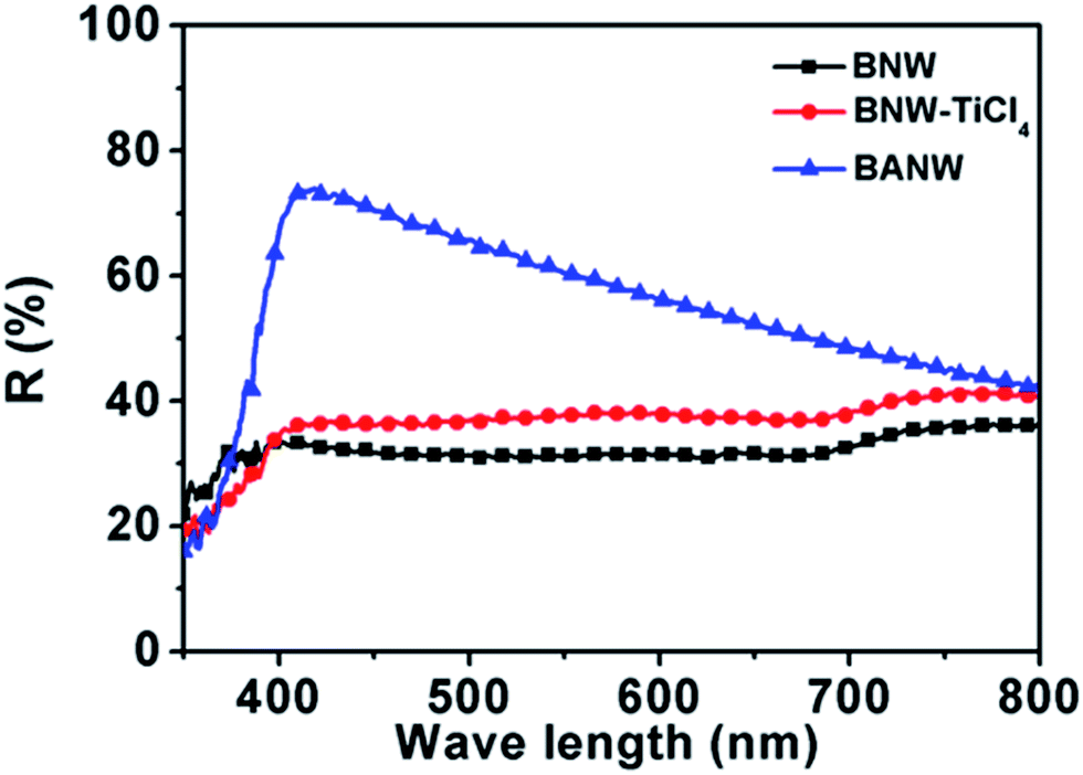 | ||
| Fig. 4 Diffuse reflectance spectra of BNW, BNW–TiCl4, and BANW photoanode film without dye loading, respectively. | ||
It should be noted that the increase of Jsc is biggish after the formation of the mixed-phase structure. The Jsc of BNW–TiCl4 cell was nearly two times higher than that of the bare BNW cell, and was further improved to over four times for the BANW cell. TiCl4 treatment can help to improve the Jsc of anatase TiO2 photoanodes since it can modify the surface defects and facilitate electron transport, but the efficacy was somehow limited.33,34 Except for the enhanced LHE, the massive increase of Jsc can be attributed to the enhanced driving force for electron injection and transport which resulted from the mixed-phase structure of TiO2–B/anatase composite photoanode. It has been reported that TiO2–B has a little smaller band gap than anatase phase, which can drive the electron transfer from anatase phase to TiO2–B.19 As illustrated in Scheme 1, the photo-generated electrons injected into the conductive band (CB) of the anatase nanoparticle shell can be transferred to the CB of TiO2–B. This driving force can facilitate the electron separation and transport that leads to an enhanced ηcc, which is also beneficial to the Jsc value. This assumption can be confirmed by an electron dynamic study which was further discussed below. In addition to the Jsc, the mixed-phase composite structure also helped to increase the Voc value. As mentioned before, the composite structure can provide a large amount of dye molecules to absorb incident light to generate photoelectrons. Compared to pure TiO2–B, the heterojunction energy band structure and electron accumulation on the CB of composite TiO2 would induce the quasi-Fermi level shifting negatively, and as a result, the Voc of the composite photoanode based cell should increase, given that the Voc of DSSCs is determined by the difference between the Fermi level of the semiconductor photoanode and the redox potential of the electrolyte.37 In the BANW photoanode a thick layer of anatase particles attached tightly to the surface of the TiO2–B nanowires, and the driving force for electron transport as well as energy band shift should be enhanced. That is why the Voc was improved from 706 mV for BNW to 718 mV for BNW–TiCl4, and further to 756 mV for BANW.
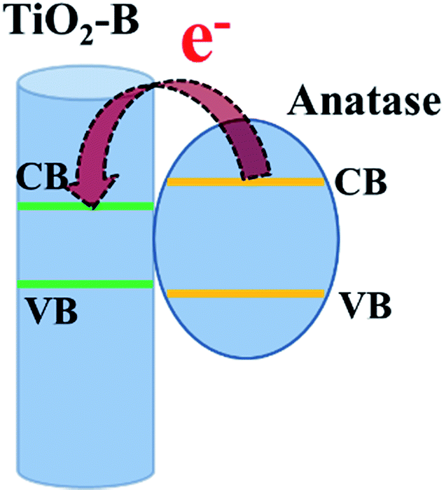 | ||
| Scheme 1 Schematic diagram of the electron transfer process in the TiO2–B/anatase core–shell photoanode. | ||
To further understand the influences of the mixed-phase structure on nanowire array photoanodes, the electrochemical impedance spectroscopy (EIS) measurement was carried out. Fig. 5 shows the Nyquist plots of the cells based on the BNW, BNW–TiCl4, and BANW photoanodes. The bigger semicircle at the middle frequency range refers to an electron transfer process at the TiO2/dye/electrolyte interface.38 By using an equivalent circuit containing resistance (R) and a constant phase element (CPE) (Fig. 5, inset), the electron recombination resistance was fitted to be 569.3 Ω, 316.8 Ω, and 111.8 Ω for the BNW, BNW–TiCl4 and BANW cells, respectively. This indicated that the greatest electron recombination happened in the BANW cell, while the pristine BNW cell showed the weakest recombination. This is because the smooth surface of the bare TiO2–B nanowire had fewer surface defects for electron recombination. When coating with anatase nanoparticles, the surface defects and trapping sites were increased greatly, which would undoubtedly increase the electron recombination possibility. Since the BANW structure had a thicker nanoparticle shell, the electron recombination was the greatest. The electron lifetime of the three cells, estimated by τn = R2 × CPE2, was 0.63 s, 0.39 s, and 0.10 s for the BNW, BNW–TiCl4 and BANW cells, respectively, further confirming that the BANW structure showed the greatest electron recombination. Generally, it is believed that high electron recombination and a shorter electron lifetime will lead to a decrease in Voc. However, the Voc of the three cells exhibited a reverse order, that is BANW > BNW–TiCl4 > BNW. This suggested that the energy band negative shift induced by the mixed-phase structure played a dominant role in affecting the Voc value. Although the electron recombination possibility in the BANW was large, the anatase shell can elevate the Fermi level immensely to get a high Voc.
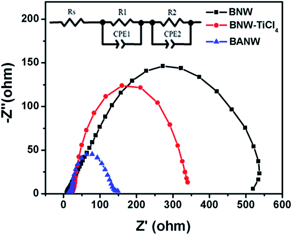 | ||
| Fig. 5 Nyquist plots of cells based on the BNW, BNW–TiCl4, and BANW photoanode, respectively. Inset is the equivalent circuit used to fit the plots by Z-view software. | ||
The electron transport dynamics in the composite structure photoanode was further examined by intensity-modulated photocurrent/photovoltage spectroscopy (IMPS/IMVS), which has been proven to be an effective way to disclose the charge transport mechanism in DSSCs.39 Fig. 6 shows the curves of electron transport time (τd) and electron lifetime (τr) of different cells as the function of incident light intensity. Here, τd (τr) is calculated from the formula τd = 1/2πfIMPS (τr = 1/2πfIMVS), where fIMPS (fIMVS) is the characteristic frequency of the minimum IMPS (IMVS) imaginary component. Surprisingly, the BNW cell showed the longest transport time although it had the fewest surface defects and trapping sites, while the BANW cell gave the shortest transport time (Fig. 6a). It means that the electron transport rate was the fastest in the BANW cell. This phenomenon is attributed to the energy band difference of the TiO2–B/anatase composite structure which may facilitate the electron transfer and transport. In addition, the larger dye-loading amount of the mixed-phased composite structure, especially the BANW photoanode, can generate a higher photoelectron density on the CB of TiO2, which may also accelerate the fast electron transport. To gain better insight into the electron transport within composite photoanodes, the electron diffusion coefficient (Dn) was calculated via the expression: Dn = d2/(4τd). As plotted in Fig. 6d, the Dn value of all cells increases with the raising of light intensity, while the BANW cell shows the highest value and the BNW–TiCl4 cell also shows a higher value than the BNW cell. This means that the electron transport was faster within the TiCl4-treated BNW photoanode although only a thin layer of nanoparticles was formed on the TiO2–B nanowires; when a thick anatase nanoparticle shell formed, the electron transport capability was enhanced further. This result further verified the statement that the TiO2–B/anatase mixed-phase structure can accelerate the electron transport. On the other hand, the electron lifetime of the three cells showed a reverse order as BANW < BNW–TiCl4 < BNW (Fig. 6b). This can be attributed to the adverse effects of nanoparticle decoration on the shell which may provide more surface reaction sites for electron recombination. This result is highly consistent with the EIS study. As a consequence, the charge collection efficiency (ηcc) of different cells was calculated according to the formula ηcc = 1 − (τd/τr).40 Fig. 6c shows the ηcc curves as the function of incident light intensity. The electron collection in the BNW cell was a little inefficient and the value decreased with increasing light intensity. After being treated with TiCl4, the collection capability of the composite photoanode based cell was obviously raised, and the BANW cell showed the best ηcc value. The high electron collection efficiency should contribute a lot to the Jsc value,35 which agreed well with the photovoltaic measurement. Therefore, it can be concluded that the hierarchical TiO2–B/anatase core/shell mixed-phase structure can provide a strong light harvesting ability, and also have fast electron transport and a high electron collection efficiency, thus leading to a higher conversion efficiency than the pristine TiO2–B photoanode.
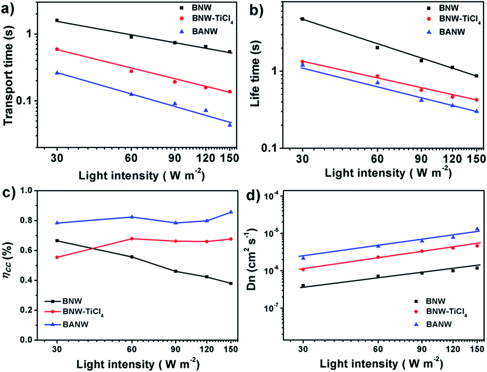 | ||
| Fig. 6 Electron transport time (a), electron lifetime (b), electron collection efficiency (c) and electron diffusion coefficients (d) as the function of the incident light intensity of DSSCs based on different photoanodes. | ||
4. Conclusion
In this work, hierarchical TiO2–B/anatase core/shell nanowire arrays on a titanium plate substrate are synthesized via a hydrothermal reaction combined with a calcination process. Such a hierarchical composite structure can provide an enlarged surface area for dye adsorption and effective light scattering, thus leading to a high photo-generated current density when used as a photoanode for DSSCs. In addition, the electron transport and recombination investigation reveals that the composite photoanode exhibits more serious electron recombination but faster electron transport than the pristine TiO2–B nanowire array photoanode. The fast electron transport should be attributed to the larger light utilizing ability and the energy band difference between the mixed-phase structure which can facilitate the electron transfer and transport. Therefore, a high electron collection efficiency is obtained for the composite photoanode based cell. As a result, both the Jsc and Voc of the hierarchical composite photoanode based cell are greatly enhanced and an η of 4.88% is obtained which is attributed to the strong light harvesting capability, fast electron transport and high electron collection efficiency. This value is among the highest reported value of TiO2 nanowire array photoanodes grown on a titanium plate substrate, which is believed to be improved further by replacing the opaque metal plate with a transparent conductive glass substrate suitable for front-side illumination devices.Acknowledgements
The authors acknowledge financial support from the National Natural Science Foundation of China (51472274, 21103236), the Pearl River S&T Nova Program of Guangzhou (2014J2200025), the Program of Guangzhou Science and Technology (2014J4100016, 201504010031), the NSF of Guangdong Province (S2013030013474) and the Research Fund for the Doctoral Program of Higher Education (20110171120026).Notes and references
- B. O’Regan and M. Grätzel, Nature, 1991, 353, 737–740 CrossRef.
- G. Calogero, A. Bartolotta, G. Di Marco, A. Di Carlo and F. Bonaccorso, Chem. Soc. Rev., 2015, 44, 3244–3294 RSC.
- H.-Y. Chen, D.-B. Kuang and C.-Y. Su, J. Mater. Chem., 2012, 22, 15475–15489 RSC.
- X. Lai, J. E. Halpert and D. Wang, Energy Environ. Sci., 2012, 5 Search PubMed.
- Q. F. Zhang and G. Z. Cao, Nano Today, 2011, 6, 91–109 CrossRef CAS.
- A. Pang, X. Sun, H. Ruan, Y. Li, S. Dai and M. Wei, Nano Energy, 2014, 5, 82–90 CrossRef CAS.
- T. P. Chou, Q. Zhang, B. Russo, G. E. Fryxell and G. Cao, J. Phys. Chem. C, 2007, 111, 6296–6302 CAS.
- J. Nelson and R. E. Chandler, Coord. Chem. Rev., 2004, 248, 1181–1194 CrossRef CAS.
- J. van de Lagemaat, N. G. Park and A. J. Frank, J. Phys. Chem. B, 2000, 104, 2044–2052 CrossRef CAS.
- B. Liu and E. S. Aydil, J. Am. Chem. Soc., 2009, 131, 3985–3990 CrossRef CAS PubMed.
- X. Feng, K. Shankar, O. K. Varghese, M. Paulose, T. J. Latempa and C. A. Grimes, Nano Lett., 2008, 8, 3781–3786 CrossRef CAS PubMed.
- J.-Y. Liao, B.-X. Lei, H.-Y. Chen, D.-B. Kuang and C.-Y. Su, Energy Environ. Sci., 2012, 5, 5750–5757 CAS.
- W.-Q. Wu, H.-S. Rao, H.-L. Feng, X.-D. Guo, C.-Y. Su and D.-B. Kuang, J. Power Sources, 2014, 260, 6–11 CrossRef CAS.
- J. Qu, G. R. Li and X. P. Gao, Energ. Environ. Sci., 2010, 3, 2003–2009 RSC.
- C. Magne, F. Dufour, F. Labat, G. Lancel, O. Durupthy, S. Cassaignon and T. Pauporté, J. Photochem. Photobiol., A, 2012, 232, 22–31 CrossRef CAS.
- T. B. Lan, J. Dou, F. Y. Xie, P. X. Xiong and M. D. Wei, J. Mater. Chem. A, 2015, 3, 10038–10044 CAS.
- A. R. Armstrong, G. Armstrong, J. Canales, R. Garcia and P. G. Bruce, Adv. Mater., 2005, 17, 862–865 CrossRef CAS.
- J. F. Zhu, J. L. Zhang, F. Chen and M. Anpo, Mater. Lett., 2005, 59, 3378–3381 CrossRef CAS.
- D. Yang, H. Liu, Z. Zheng, Y. Yuan, J.-c. Zhao, E. R. Waclawik, X. Ke and H. Zhu, J. Am. Chem. Soc., 2009, 131, 17885–17893 CrossRef CAS PubMed.
- B. Liu, A. Khare and E. S. Aydil, ACS Appl. Mater. Interfaces, 2011, 3, 4444–4450 CAS.
- W. Li, Y. Bai, W. Zhuang, K.-Y. Chan, C. Liu, Z. Yang, X. Feng and X. Lu, J. Phys. Chem. C, 2014, 118, 3049–3055 CAS.
- K. Pan, Q. L. Zhang, Q. Wang, Z. Y. Liu, D. J. Wang, J. H. Li and Y. B. Bai, Thin Solid Films, 2007, 515, 4085–4091 CrossRef CAS.
- L. H. Qi, Y. J. Liu and C. Y. Li, Appl. Surf. Sci., 2010, 257, 1660–1665 CrossRef CAS.
- K. Pan, Y. Z. Dong, W. Zhou, G. F. Wang, Q. J. Pan, Y. Yuan, X. H. Miao and G. H. Tian, Electrochim. Acta, 2013, 88, 263–269 CrossRef CAS.
- Y. Z. Dong, K. Pan, G. H. Tian, W. Zhou, Q. J. Pan, T. F. Xie, D. J. Wang and H. G. Fu, Dalton Trans., 2011, 40, 3808–3814 RSC.
- B. Ohtani, O. O. Prieto-Mahaney, D. Li and R. Abe, J. Photochem. Photobiol., A, 2010, 216, 179–182 CrossRef CAS.
- D. C. Hurum, A. G. Agrios, K. A. Gray, T. Rajh and M. C. Thurnauer, J. Phys. Chem. B, 2003, 107, 4545–4549 CrossRef CAS.
- T. Kawahara, Y. Konishi, H. Tada, N. Tohge, J. Nishii and S. Ito, Angew. Chem., Int. Ed., 2002, 41, 2811–2813 CrossRef CAS.
- H. Y. Zhu, Y. Lan, X. P. Gao, S. P. Ringer, Z. F. Zheng, D. Y. Song and J. C. Zhao, J. Am. Chem. Soc., 2005, 127, 6730–6736 CrossRef CAS PubMed.
- L. B. Yang, Y. Zhang, W. D. Ruan, B. Zhao, W. Q. Xu and J. R. Lombardi, J. Raman Spectrosc., 2010, 41, 721–726 Search PubMed.
- A. R. Armstrong, G. Armstrong, J. Canales and P. G. Bruce, Angew. Chem., Int. Ed., 2004, 43, 2286–2288 CrossRef CAS PubMed.
- C. J. Barbé, F. Arendse, P. Comte, M. Jirousek, F. Lenzmann, V. Shklover and M. Grätzel, J. Am. Ceram. Soc., 1997, 80, 3157–3171 CrossRef.
- P. M. Sommeling, B. C. O’Regan, R. R. Haswell, H. J. P. Smit, N. J. Bakker, J. J. T. Smits, J. M. Kroon and J. A. M. van Roosmalen, J. Phys. Chem. B, 2006, 110, 19191–19197 CrossRef CAS PubMed.
- N. Fuke, R. Katoh, A. Islam, M. Kasuya, A. Furube, A. Fukui, Y. Chiba, R. Komiya, R. Yamanaka, L. Y. Han and H. Harima, Energy Environ. Sci., 2009, 2, 1205–1209 Search PubMed.
- K. Zhu, N. R. Neale, A. Miedaner and A. J. Frank, Nano Lett., 2007, 7, 69–74 CrossRef CAS PubMed.
- G. Veerappan, D. W. Jung, J. Kwon, J. M. Choi, N. Heo, G. R. Yi and J. H. Park, Langmuir, 2014, 30, 3010–3018 CrossRef CAS PubMed.
- J. Bandara and U. W. Pradeep, Thin Solid Films, 2008, 517, 952–956 CrossRef CAS.
- F. Fabregat-Santiago, J. Bisquert, E. Palomares, L. Otero, D. Kuang, S. M. Zakeeruddin and M. Grätzel, J. Phys. Chem. C, 2007, 111, 6550–6560 CAS.
- H. Wang, P. G. Nicholson, L. Peter, S. M. Zakeeruddin and M. Grätzel, J. Phys. Chem. C, 2010, 114, 14300–14306 CAS.
- Y.-F. Wang, K.-N. Li, W.-Q. Wu, Y.-F. Xu, H.-Y. Chen, C.-Y. Su and D.-B. Kuang, RSC Adv., 2013, 3, 13804–13810 RSC.
| This journal is © The Royal Society of Chemistry 2016 |