
Effect of Zn substitution at a Cu site on the transport behavior and thermoelectric properties in Cu3SbSe4†
Aparabal Kumar,
P. Dhama,
Deepash S. Saini and
P. Banerji*
Materials Science Centre, Indian Institute of Technology, Kharagpur 721302, India. E-mail: pallab@matsc.iitkgp.ernet.in; Tel: +91 3222 283984
First published on 7th January 2016
Abstract
An attempt is made in this study to find the effect of substitution of Zn at a Cu site in copper antimony selenide (Cu3−xZnxSbSe4; x = 0, 0.5, 1.0), prepared using a conventional melt growth followed by spark plasma sintering, with the aim of investigating the transport behavior and thermoelectric properties. A single parabolic band model with acoustic phonon scattering approximation was used to explain the transport phenomenon and density of states effective mass. The intrinsic samples (x = 0) show unipolar transport with holes as majority charge carriers. It was found that both the effective mass and carrier concentration decreased with increase in Zn concentration. From thermal conductivity measurements, evidence of bipolar carrier transport is found above 475 K in Zn containing samples and thus the possibility of involvement of other scattering mechanisms along with acoustic phonons is not ruled out. The Seebeck coefficient of the samples containing Zn show a negative value above 600 K whereby it is observed that substitution of Cu with Zn contributes electronic charge carriers in Cu3−xZnxSbSe4. The value of the thermoelectric figure of merit (ZT) in Zn substituted samples first increases till 475 K and then starts to decrease sharply due to bipolar charge transport, however, Cu2.5Zn0.5SbSe4 (x = 0.5) shows the highest ZT compared to other samples.
1 Introduction
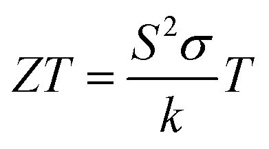
Waste heat recovery is an essential step to cope with limited sources of conventional energy together with its higher demand. One of the emerging and non-conventional areas is thermoelectricity.1–3 Thermoelectric materials play an important role in converting waste heat into electricity.4,5 The efficiency of these materials is represented by a dimensionless parameter called the thermoelectric figure of merit (ZT), and is given by
 | (1) |
Since all the above parameters are interrelated and change in one parameter will affect the value of the other, it is a challenging task to optimize the thermoelectric figure of merit just by changing one parameter. Such as reducing the value of electronic contribution of thermal conductivity (ke) in effect reduces the value of the electrical conductivity (σ) which is not desired. Thus to optimize ZT, the best option is to reduce the value of the thermal conductivity (k) by reducing the contribution of kl. One of the best ways to reduce the value of kl is to use the concept of electron crystal – phonon glass where electrons can move throughout the lattice and phonon will be scattered by several scattering centers as is happened during the movement of the phonon in the glass.6,7 Several approaches have been adopted to optimize the thermoelectric figure of merit by optimizing the lattice thermal conductivity using various concepts such as modification in the band structure, grain boundary scattering, quantum confinement effect, strained endotaxial structure, band convergence, nanostructuring, etc.8–14
For the selection of a material for commercial application, it is expected that it should be cheaper, highly abundant in the earth crust, environment-friendly as well as high efficiency (thermoelectric figure of merit). Till date PbTe is the best polycrystalline thermoelectric material with maximum reported thermoelectric figure of merit,15 however, lead is toxic, and tellurium is less abundant. Thus worldwide various research groups have been trying to find lead and tellurium free thermoelectric materials to achieve a reasonable value of ZT. Thermoelectric studies on Cu–Sb–Se based compounds are reported for the phases Cu3SbSe3, Cu3SbSe4, and CuSbSe2.16–20 Though complete phase diagram of Cu–Sb–Se based system is still not established which is essential to understand its properties,16 Cu3SbSe4 is one of the best thermoelectric materials as it shows good thermoelectric behavior near 675 K.21–28 Despite the fact that Cu3SbSe4 is a potential thermoelectric material, very few experimental studies on this material is reported. To understand low lattice thermal conductivity in the ternary Cu–Sb–Se system, Zhang et al. performed the first principle calculation based on density functional theory and found that lattice anharmonicity plays a major role behind this.17 Do et al. theoretically studied the effect of substitution and doping in Cu3SbSe4 at different sites and predicted the band structure using first principle density functional theory.29 The authors reported that Se site always possesses large positive formation energy whereas Cu site shows negative formation energy for Na, Mg and Zn, and Sb site for Ti, V, Ge, Sn, and Pb. To improve the transport properties as well as the value of ZT, further modification like doping, alloying, nanostructuring and nano-inclusion in Cu3SbSe4 structure is proposed.23
Formation of impurity level near the band edge is desired in the materials since it will allow thermal excitation of charge carriers. Cu3SbSe4 is suitable in this respect as its activation energy are smaller than its band gap (∼0.3 eV) due to formation of defect level inside its band gap.30 To tune the properties we have adopted the technique of substitution of an element by another with a small difference in atomic and ionic radii. In this work, we have thus attempted to study the effect of zinc substituted copper antimony selenide (Cu3−xZnxSbSe4 for x = 0, 0.5, and 1.0) on its thermoelectric properties where Zn substitutes Cu atom in copper antimony selenium alloy. Ionic radius of Zn (Zn2+) is almost same as that of Cu. When Zn substitutes Cu in Cu3SbSe4, it is expected that some of the Zn (or Cu) atoms will form secondary phases inside the material due to the difference in their valence electron structures. The amount of secondary phase will increase with increase in Zn content. Thus additional phonon scattering will take place due to the disordered arrangement of secondary phases inside Cu3SbSe4 which should reduce the value of the thermal conductivity.
2 Experimental
2.1 Synthesis
For the investigation and analysis of thermoelectric properties in Cu3−xZnxSbSe4 (with x = 0, 0.5 and 1.0), high purity lump (6N, Alfa Aesar) of elemental Cu, Sb, Se and Zn were used as source materials. Each of the elements were first etched with their suitable etchant to remove surface oxide layer, if any, and then rinsed with methanol and deionized water after which it is kept in a vacuum furnace to remove moisture. The cleaned materials were weighted with proper stoichiometric ratio and kept in ampoules evacuated to 10−6 Torr before sealing. Double ampoule (i.e. one ampoule with smaller diameter containing the elements was put inside another ampoule of larger diameter) sealing was made to overcome the problem of difference in thermal expansion coefficient of the materials and ampoule during solidification. After sealing, the ampoules were placed in a vertical furnace. The temperature of the furnace was slowly raised to 1200 °C and kept at this temperature for 24 h to homogenize the melt. Then the temperature was reduced at a rate of 20 °C h−1 to 500 °C and was kept at this temperature for next 24 h after which the furnace was switched off for room temperature cooling. The obtained cylindrical ingots of diameter 10 mm by this process were first annealed for 72 h at 250 °C under vacuum to achieve the desirable (single) phase of grown materials and then pulverized into fine particles using an agate mortar followed by planetary ball milling. The resulting powder was sintered under vacuum by spark plasma sintering (Fuji Electronic) at 300 °C and 65 MPa for 7 min using a graphite die of 10 mm central opening diameter. The density of the samples was determined using Archimedes' principle was found to be around 90% of the theoretical density. The pellets were used for structural analysis and measurements of thermal and electrical transport properties. For Seebeck coefficient measurements, bar-shaped samples of size 1.3 × 1.2 × 8 mm3 were prepared by cutting the pellets using a low speed saw diamond cutter (Isomet) after carrying out resistivity and Hall measurements.2.2 Structural characterization
Phase analysis of the materials was carried out by powder X-ray diffraction of the samples (PANalytical – X'PertPro X-ray diffractometer) for 2θ scan operated at 20 mA and 40 kV, using Ni-filtered Cu Kα radiation (λ = 1.54056 Å) in reflection geometry, equipped with a position sensitive detector. The XRD was performed for 2θ value between 15–80 degree with a small step and low scanning speed and the obtained data were analyzed using Rietveld refinement. For transmission electron microscopic (TEM) analysis, samples were prepared by conventional polishing and dimpling, followed by argon-ion milling at liquid nitrogen temperature. TEM investigations were carried out using a JEOL JEM 2100 machine operated at an accelerating voltage of 200 kV. The surface morphology was analyzed by a Field Emission Scanning Electron Microscope (FESEM) (Zeiss, Merlin – Gemini II). High resolution X-ray photoelectron spectroscopy (XPS) was employed to analyze the chemical state of the samples by using a PHI 5000 VersaProbe II (ULVAC-PHI, Japan) system connected with a microfocused (100 μm, 25 W, 15 kV) monochromatic Al Kα source (hν = 1486.6 eV), a hemispherical electron energy analyzer, and a multichannel detector.2.3 Electrical characterization
Electrical resistivity (ρ) and Hall measurements were carried out under van der pauw configuration in the temperature range 300–625 K in the nitrogen ambient to avoid oxidation. Hall measurement was carried out in the presence of 1.0 T magnetic field. Seebeck coefficient measurements were carried out where a bar-shaped sample was placed between the spring assisted copper heating blocks of diameter 8 mm under dynamic vacuum.312.4 Thermal characterization
Thermal conductivity measurements were carried out using Hot Disk – thermal constant analyzer (TPS-2500S). Double sided isotropic transient measurement was performed in the temperature range 300–625 K under dynamic vacuum where the sample was adjusted on high temperature sample holder fitted with tubular furnace.3 Results and discussion
The crystal structure, crystallite size, and phase purity were studied using X-ray diffractogram (XRD). To identify the crystallographic symmetry of Cu3−xZnxSbSe4 (x = 0, 0.5 and 1.0), Rietveld refinement was carried out using the diffraction data obtained at room temperature. The XRD pattern of the samples are shown in Fig. 1.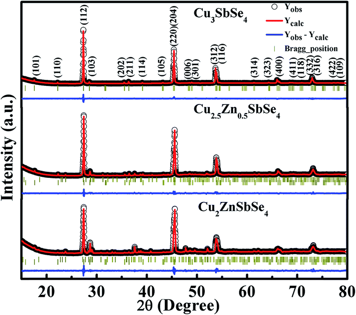 | ||
| Fig. 1 X-ray diffractogram of Cu3−xZnxSbSe4 with x = 0, 0.5 and 1.0. | ||
All the major peaks are indexed with refined data. It was found that the samples show tetragonal crystal structure with space group I![[4 with combining macron]](https://www.rsc.org/images/entities/char_0034_0304.gif) 2m and high phase purity was observed in intrinsic sample (x = 0). The XRD pattern of the samples with the addition of Zn clearly consists of more diffraction peaks (though with very low intensity) than intrinsic sample around 30–40 degree and seems to contain a considerable amount of secondary phases. Samples containing Zn was refined with two space groups, i.e. I2m of Cu3SbSe4 with tetragonal, and secondary phase of CuSbSe2 with Pnma space group and orthorhombic crystal structure. Refined structural parameters in Cu3−xZnxSbSe4 for x = 0, 0.5 and 1.0 are compiled in the ESI file in Tables S1–S3† respectively. The crystal structure of the intrinsic sample, i.e. x = 0 was obtained using Diamond software and shown in Fig. 2. The crystallite size of the samples was calculated using Scherrer formula. The value of crystallite size was found to be within 20–30 nm. Small crystallite is advantageous for thermoelectric applications as it helps to reduce the value of thermal conductivity by scattering long wavelength phonon.
2m and high phase purity was observed in intrinsic sample (x = 0). The XRD pattern of the samples with the addition of Zn clearly consists of more diffraction peaks (though with very low intensity) than intrinsic sample around 30–40 degree and seems to contain a considerable amount of secondary phases. Samples containing Zn was refined with two space groups, i.e. I2m of Cu3SbSe4 with tetragonal, and secondary phase of CuSbSe2 with Pnma space group and orthorhombic crystal structure. Refined structural parameters in Cu3−xZnxSbSe4 for x = 0, 0.5 and 1.0 are compiled in the ESI file in Tables S1–S3† respectively. The crystal structure of the intrinsic sample, i.e. x = 0 was obtained using Diamond software and shown in Fig. 2. The crystallite size of the samples was calculated using Scherrer formula. The value of crystallite size was found to be within 20–30 nm. Small crystallite is advantageous for thermoelectric applications as it helps to reduce the value of thermal conductivity by scattering long wavelength phonon.
 | ||
| Fig. 2 Crustal structure of Cu3SbSe4. | ||
Field emission scanning electron spectroscopy (FESEM) has been employed to study the surface morphology of the materials. The micrographs are shown in Fig. 3(a) for policed and etched surface, whereas Fig. 3(b)–(d) are for the fractured surface of plasma sintered Cu3SbSe4, Cu2.5Zn0.5SbSe4 and Cu2ZnSbSe4, respectively. Fig. 3(b)–(d) indicate that the sintered samples due to its dense texture could be useful for the thermoelectric application. It is clearly observed that no grain growth has taken place in sintered samples which is required to reduce the value of thermal conductivity by phonon scattering due to smaller particle size within the samples.
 | ||
| Fig. 3 FESEM image of (a) polished and etched surface, whereas (b), (c) and (d) are for the fractured surface of spark plasma sintered Cu3SbSe4, Cu2.5Zn0.5SbSe4, and Cu2ZnSbSe4, respectively. | ||
Further studies on chemical analysis of the samples Cu3−xZnxSbSe4 with x = 0 and 1.0 were carried out using high resolution XPS and the obtained (narrow) spectra of the elements were fitted using XPSPEAK41 and are shown in Fig. 4. Carbon (C 1s) was used as a reference material with corresponding bonding energy 284.6 eV for XPS identification. In Cu3SbSe4, the core level of Cu 2p, Sb 3d, and Se 3d were examined. It was found that Cu 2p core level splits into two strong intense peaks, i.e. Cu 2p3/2 (932.2 eV) and Cu 2p1/2 (952.1 eV) with splitting energy 19.9 eV which suggest that Cu in Cu3SbSe4 is (+1) oxidation state.32 Similarly the experimental data of the core level of antimony was fitted with doublet intense peak (Sb 3d5/2 and Sb 3d1/2) with binding energy 529 eV and 538.4 eV, respectively, and spin–orbit splitting (SOS) of 9.4 eV. Presence of Se 3d peak at 54.1 eV confirms the existence of Se in the (−2) state in the sample. In Cu2ZnSbSe4 spectra, the existence of Cu, Sb and Se peaks were observed with same spin orbital splitting and nearly same binding energy except the presence of Zn peak in the later. Zinc is also giving two intense peaks, i.e. Zn 2p1/2 and Zn 2p3/2 with binding energy 1043.8 eV and 1020.7 eV, respectively, and SOS 23.1 eV. From XPS analysis, it is confirmed that all the constitute elements are present in the samples.
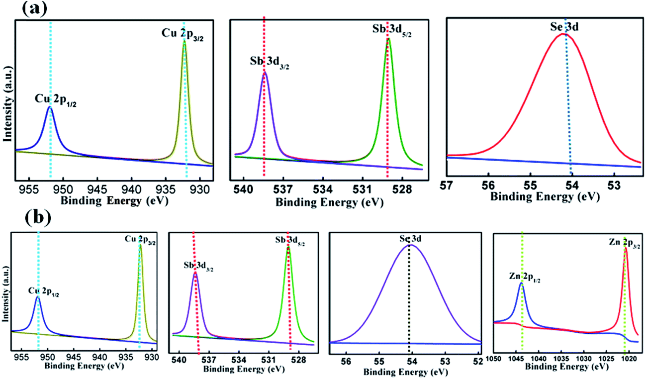 | ||
| Fig. 4 X-ray photoelectron spectra of (a) Cu3SbSe4, and (b) Cu2ZnSbSe4. | ||
For studying further the microstructure in Cu3−xZnxSbSe4 with x = 0 and 1.0, transmission electron microscopy (TEM) was employed and the micrograph is shown in Fig. 5. From the lattice fringes, it was found that the lattice spacing in Cu3SbSe4 (x = 0) is 3.19 Å which is closely matched to (112) plane with JCPDS file of pdf # 85-0003. Similarly, the lattice spacing of 3.057 Å corresponds to (103) plane and 3.34 Å corresponds to (112) plane in case of Cu2ZnSbSe4 (x = 1.0) and matches with the same JCPDS file. The selected area electron diffraction (SAED) pattern (shown in inset) shows the samples are polycrystalline.
 | ||
| Fig. 5 Bright field TEM image of (a) Cu3SbSe4, and (b) Cu2ZnSbSe4 with SAED pattern shown in inset. | ||
Temperature dependent electrical resistivity in Cu3−xZnxSbSe4 with x = 0, 0.5 and 1.0 are shown in Fig. 6(a). In case of Cu3SbSe4 (x = 0), unipolar charge carriers, i.e. the holes, take part in the transport process. When temperature is increased, the resistivity of the intrinsic samples is found to decrease throughout the temperature range measured (300–650 K) due to thermal excitation of charge carriers and shows typical non-degenerate semiconducting behavior. It was observed that the electrical resistivity of the intrinsic sample (x = 0) was lower than that of the samples with partial substitution of Cu by Zn in Cu3SbSe4. It is due to scattering of charge carriers via secondary phases present in the samples containing Zn. The increase in electrical resistivity in Zn content samples compared to intrinsic one can also be expected by neutralization (compensation) of holes (majority carriers in Cu3−xZnxSbSe4 with x > 0) by the electrons coming from the thermal excitation of Zn. Although in case of Cu3−xZnxSbSe4 with x > 0, resistivity does not decrease linearly, the nonlinear behavior, observed at 475 K, could be attributed to the bipolar charge transport in the samples. This was later confirmed by the thermal conductivity measurements.
 | ||
| Fig. 6 (a) Plot of electrical resistivity as a function of temperature (b) logarithmic resistivity vs. inverse of temperature (c) temperature dependent Seebeck coefficient, and (d) temperature dependent power factor. | ||
A good linearity was observed when the logarithmic value of resistivity was plotted as a function of reciprocal of temperature till 475 K for Cu3−xZnxSbSe4 with x = 0.5 and 1.0, as shown in Fig. 6(b). From the Arrhenius plot and fitting the experimental data, the value of activation energy in Cu3−xZnxSbSe4, for x = 0, 0.5 and 1.0, was determined and found to be 0.130 eV, 0.091 eV and 0.076 eV, respectively. It can be understood by using the concept of impurity level formed via doping in semiconducting materials. When Cu is substituted by Zn, it will form donor level near the conduction band and with more Zn content, as shallow impurity level will be formed leading to an effective decrease in the value of energy band gap. This has been confirmed by the XRD data. It is found that small difference in size of Zn and Cu ions creates distortion in the lattice and increases the value of the lattice constants (a and c in case of Cu3SbSe4), which in turn decreases the value of energy gap.
Thermal conductivity of all the samples is shown in Fig. 7. Since the optical phonon has a negligible role in heat transport in non-metals due to their weaker dispersion compared to acoustic phonon, thermal conductivity can be decreased by reducing heat transfer via acoustic term of lattice vibration. Heat transport is directly dependent on the mean free path (l) of phonon and the value of l is temperature dependent and above room temperature l ∝ 1/T. The experimentally obtained thermal conductivity shows a variation of T−1 which represents the dominant scattering mechanism as phonon–phonon interaction in the studied temperature range in the intrinsic samples. In Zn substituted samples, it was observed that above 475 K, there is a deviation from T−1 variation. Thus, some other scattering mechanisms involved along with acoustic phonon scattering. From the resistivity measurements, strong evidence of bipolar transport is found above 475 K in Zn substituted samples. Thus single parabolic band (SBP) model is not appropriate to explain this transport behavior in the samples containing Zn above this temperature (475 K). By Zn addition, the thermal conductivity of the samples decreases greatly. It may be due to decrease in the electronic contribution of thermal conductivity as a result of scattering of electrons by the small amount of secondary phase that exists in Zn containing samples, as well as the scattering of acoustic phonon via secondary phases, and a difference in atomic and ionic radii in Cu and Zn. It was observed from the experimental data that the sample with x = 0.5 shows lower thermal conductivity whereas the intrinsic one has maximum thermal conductivity. It is due to scattering of acoustic phonons via substitutional impurities in the crystal lattice with asymmetric occupancy of Zn at Cu-1 site for x = 0.5. In the case of x = 1, all the Cu-1 sites of Cu3SbSe4 are occupied by Zn and shows less asymmetric behavior compared to x = 0.5 and hence shows the higher value of thermal conductivity than that of Cu2.5Zn0.5SbSe4.
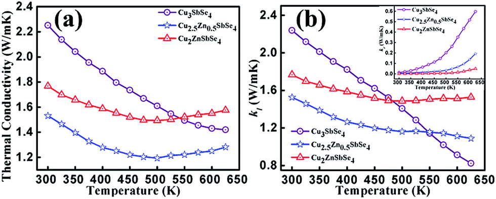 | ||
| Fig. 7 Temperature dependent (a) total thermal conductivity, and (b) lattice thermal conductivity (electronic contribution of thermal conductivity is shown in inset). | ||
The electronic contribution of thermal conductivity (ke) was calculated using Wiedemann–Franz law as given below
| ke = LσT = L(neμ)T | (2) |
 | (3) |
 | (4) |
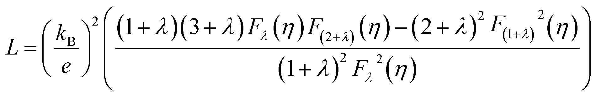
The limitation of eqn (3) is that it is applicable only for single parabolic band (SPB) with acoustic phonon scattering (APS) approximation where it is assumed that only one type of carrier is dominant and there is no influence of minority charge carrier in charge transport. For acoustic phonon scattering, the value of λ become 0 and simplifies eqn (3). If only SPB-APS approximation is considered, the value of L can be obtained following Kim et al.,34 and is given by
 | (5) |
The value of L from eqn (5) was used to calculate the value of electronic contribution of thermal conductivity neglecting a possible error due to bipolar effect in Zn containing samples above 475 K, and is plotted in the inset of Fig. 7(b). The variation of lattice contribution of thermal conductivity can be estimated by subtracting electronic contribution term from total thermal conductivity (kl = k − ke) and its variation with temperature is shown in Fig. 7(b).
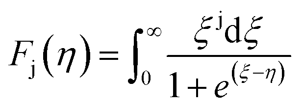
For all three samples, no influence of minority carrier transport was observed at room temperature and thus SPB model is valid to explain and calculate different electrical and thermal transport parameters. The density of states effective mass at room temperature is calculated using eqn (4), (6) and (7) shown below considering the APS approximation (λ = 0).
 | (6) |
 | (7) |
All the parameters used here are earlier defined. The value of effective mass along with other electrical parameters, viz. carrier concentration, Hall mobility, electrical resistivity and activation energy have been presented in Table 1.
| Sample | Carrier concentration (cm−3) | Hall mobility (cm2 V−1 S−1) | Electrical resistivity (Ω cm) | Activation energy (eV) | (m*/m0) |
|---|---|---|---|---|---|
| Cu3SbSe4 | 2.7674 × 10¹⁸ | 63 | 3.549 × 10⁻² | 0.130 | 0.86 |
| Cu2.5Zn0.5SbSe4 | 8.1290 × 10¹⁷ | 85 | 8.129 × 10⁻² | 0.091 | 0.78 |
| Cu2ZnSbSe4 | 1.5265 × 10¹⁷ | 102 | 4.014 × 10⁻¹ | 0.076 | 0.67 |
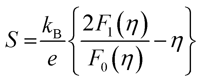
The temperature dependent Seebeck coefficient (S) is shown in Fig. 6(c). Steady state differential method was used to measure the value of S to overcome the influence of any voltage offset. The positive value of Seebeck coefficient in intrinsic Cu3SbSe4 shows holes as majority charge carriers in the samples. Here, the p-type behavior shown by Cu3SbSe4 is attributed to Cu vacancy. In the case of Cu3−xZnxSbSe4 with Zn > 0, it was found that the Seebeck coefficient is first increasing with increase in temperature and after reaching a maximum value starts to decrease sharply. This behavior of Seebeck coefficient is similar to that of electrical resistivity and it is due to thermal excitation of charge carriers. It was also found that the sample containing Zn shows bipolar transition (above 475 K) and starts showing the negative value of Seebeck coefficient after a certain temperature (>600 K). The total Seebeck coefficient (due to both electrons and holes) in case of bipolar carrier transport can be explained with the help of the following relation35
 | (8) |
Temperature dependent power factor is shown in Fig. 6(d). It was observed that the value of power factor in Cu3−xZnxSbSe4 (x = 0.5 and 1.0) is higher than that of the samples with x = 0 in the temperature range 400–525 K. Moreover, the behavior of power factor of the samples containing Zn first increases till 475 K and thereafter starts to decrease sharply as if they are following the pattern of variation in Seebeck coefficient.
The temperature dependent thermoelectric figure of merit in all the samples is shown in Fig. 8. A maximum ZT value (ZT ≈ 0.35) was observed in the samples with x = 0.5, i.e. Cu2.5Zn0.5SbSe4 at 475 K due to the relatively higher value of Seebeck coefficient and the smaller value of thermal conductivity than that of other samples. From the temperature vs. ZT plot, it is observed that ZT of the sample, in which Zn is occupying the place of Cu1 site in Cu3SbSe4, starts to decrease above 475 K. It is due to the sharp decrease in Seebeck coefficient and electrical conductivity above 475 K.
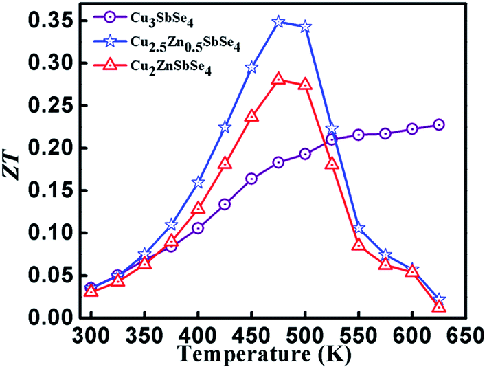 | ||
| Fig. 8 Temperature dependent thermoelectric figure of merit. | ||
4 Conclusion
Polycrystalline Cu3−xZnxSbSe4 (x = 0, 0.5 and 1) are synthesized using melt grown technique followed by planetary ball milling and spark plasma sintering (SPS). Single parabolic band (SPB) model considering acoustic phonon scattering (APS) was used to explain the transport behavior of the samples. No impurity phase was found in the intrinsic samples and very small amount of secondary phase was observed in Zn content sample. The results show that the thermal conductivity of the intrinsic sample (x = 0) is higher than that of the samples with substitution of Zn at Cu site. The lowest value of thermal conductivity is found for the samples with x = 0.5 (Cu2.5Zn0.5SbSe4) due to strong acoustic phonon scattering. The value of electrical resistivity increases with increase in Zn content which is attributed to decrease in carrier concentration. The behavior of Seebeck coefficient of Cu3SbSe4 shows the majority charge carriers are holes and carrier concentration increases with increase in temperature. In case of Cu3−xZnxSbSe4 (with x > 0), the value of Seebeck coefficient decreases sharply above 475 K due to bipolar carrier transport and above a certain specific temperature (>600 K) materials start to show n-type behavior. In this investigation, it was found that the material Cu2.5Zn0.5SbSe4 is having the highest ZT. In spite of an effective increment in the value of ZT with Zn substitution at Cu site in Cu3SbSe4, further optimization and doping at other sites are required to achieve a workable thermoelectric figure of merit for its use in commercial application.Acknowledgements
One of the authors (AK) acknowledges help of Mr Krishnendu Sarkar (Materials Science Centre, IIT Kharagpur) for XPS analysis. The authors acknowledge the DST-FIST funded XPS facility at the Department of Physics, IIT Kharagpur.References
- H. J. Goldsmid, Introduction to Thermoelectricity, Springer, Heidelberg, 2010 Search PubMed.
- Thermoelectric Handbook: Macro to Nano, ed. D. M. Rowe, CRC Taylor & Francis, Boca Raton, 2006 Search PubMed.
- D. M. Rowe, CRC handbook of Thermoelectrics, CRC Taylor & Francis, Boca Raton, 1995 Search PubMed.
- A. Shakouri, Annu. Rev. Mater. Res., 2011, 41, 399–431 CrossRef CAS.
- L. E. Bell, Science, 2008, 321, 1457–1461 CrossRef CAS PubMed.
- G. J. Snyder and E. S. Toberer, Nat. Mater., 2008, 7, 105–114 CrossRef CAS PubMed.
- L. D. Zhao, V. P. Dravid and M. G. Kanatzidis, Energy Environ. Sci., 2014, 7, 251–268 CAS.
- L. D. Zhao, S. H. Lo, Y. Zhang, H. Sun, G. Ta, C. Uher, C. Wolverton, V. P. Dravid and M. G. Kanatzidis, Nature, 2014, 508, 373–377 CrossRef CAS PubMed.
- M. G. Kanatzidis, Chem. Mater., 2010, 22, 648–659 CrossRef CAS.
- M. S. Dresselhaus, G. Chen, M. Y. Tang, R. G. Yang, H. Lee, D. Z. Wang, Z. F. Ren, J. P. Fleurial and P. Gogna, Adv. Mater., 2007, 19, 1043–1053 CrossRef CAS.
- Y. Pei, X. Shi, A. LaLonde, H. Wang, L. Chen and G. J. Snyder, Nature, 2011, 473, 66–69 CrossRef CAS PubMed.
- K. Biswas, J. Q. He, Q. C. Zhang, G. Y. Wang, C. Uher, V. P. Dravid and M. G. Kanatzidis, Nat. Chem., 2011, 3, 160–166 CrossRef CAS PubMed.
- W. Liu, X. Tan, K. Yin, H. Liu, X. Tang, J. Shi, Q. Zhang and C. Uher, Phys. Rev. Lett., 2012, 108, 166601 CrossRef PubMed.
- L. D. Hicks and M. S. Dresselhaus, Phys. Rev. B: Condens. Matter Mater. Phys., 1993, 47, 12727–12731 CrossRef CAS.
- K. Biswas, J. He, I. D. Blum, C. I. Wu, T. P. Hogan, D. N. Seidman, V. P. Dravid and M. G. Kanatzidis, Nature, 2012, 489, 414–418 CrossRef CAS PubMed.
- Y. Zhang, V. Ozolins, D. Morelli and C. Wolverton, Chem. Mater., 2014, 26, 3427–3435 CrossRef.
- Y. Zhang, E. Skoug, J. Cain, V. Ozolin, D. Morelli and C. Wolverton, Phys. Rev. B: Condens. Matter Mater. Phys., 2012, 85, 054306 CrossRef.
- K. Tyagi, B. Gahtori, S. Bathula, A. K. Srivastava, A. K. Shukla, S. Auluck and A. Dhar, J. Mater. Chem. A, 2014, 2, 15829–15835 CAS.
- D. Li and X. Y. Qin, J. Appl. Phys., 2006, 100, 023713 CrossRef.
- J. Zhou, G. Q. Bian, Q. Y. Zhu, Y. Zhang, C. Y. Li and J. Dai, J. Solid State Chem., 2009, 182, 259 CrossRef CAS.
- C. Yang, F. Huang, L. Wu and K. Xu, J. Phys. D: Appl. Phys., 2011, 44, 295404 CrossRef.
- T. R. Wei, F. Li and J. F. Li, J. Electron. Mater., 2014, 43, 2229–2238 CrossRef CAS.
- D. Li, R. Li, X. Y. Qin, C. J. Song, H. X. Xin, L. Wang, J. Zhang, G. L. Guo, T. H. Zou, Y. F. Liu and X. G. Zhu, Dalton Trans., 2014, 43, 1888–1896 RSC.
- E. J. Skoug, J. D. Cain and D. T. Morelli, Appl. Phys. Lett., 2011, 98, 261911 CrossRef.
- A. M. Fernandez and J. A. Turner, Sol. Energy Mater. Sol. Cells, 2003, 79, 391 CrossRef CAS.
- D. Do, V. Ozolins, S. D. Mahanti, M. S. Lee, Y. Zhang and C. Wolverton, J. Phys.: Condens. Matter, 2012, 24, 415502 CrossRef PubMed.
- V. B. Ghanwat, S. S. Mali, S. D. Kharade, N. B. Pawar, S. V. Patil, R. M. Mane, P. S. Patil, C. K. Hong and P. N. Bhosale, RSC Adv., 2014, 4, 51632–51639 RSC.
- K. Tyagi, B. Gahtori, S. Bathula, V. Toutam, S. Sharma, N. K. Singh and A. Dhar, Appl. Phys. Lett., 2014, 105, 261902 CrossRef.
- D. T. Do and S. D. Mahanti, J. Alloys Compd., 2015, 625, 346–354 CrossRef CAS.
- T. R. Wei, H. Wang, Z. M. Gibbs, C. F. Wu, G. J. Snyder and J. F. Li, J. Mater. Chem. A, 2014, 2, 13527 CAS.
- B. Paul, Measurement, 2012, 45, 133–139 CrossRef.
- K. Roy, C. P. Vinod and C. S. Gopinath, J. Phys. Chem. C, 2013, 117, 4717–4726 CAS.
- Materials, Preparation and Characterization in Thermoelectrics, ed. D. M. Rowe, CRC Taylor & Francis Group, Boca Raton, 2012 Search PubMed.
- H. S. Kim, Z. M. Gibbs, Y. Tang, H. Wang and G. J. Snyder, APL Mater., 2015, 3, 041506 CrossRef.
- J. H. Bahk, Z. Bian and A. Shakouri, Phys. Rev. B: Condens. Matter Mater. Phys., 2014, 89, 075204 CrossRef.
Footnote |
| † Electronic supplementary information (ESI) available. See DOI: 10.1039/c5ra21165d |
| This journal is © The Royal Society of Chemistry 2016 |