
 Open Access Article
 This Open Access Article is licensed under a
 Creative Commons Attribution 3.0 Unported Licence
Unusual crystalline morphology of Poly Aryl Ether Ketones (PAEKs)†
Yuan
Wang
*,
James D.
Beard
,
K. E.
Evans
and
Oana
Ghita
College of Engineering, Mathematics and Physical Sciences, University of Exeter, North Park Road, EX4 4QF, UK. E-mail: y.wang@exeter.ac.uk
First published on 22nd December 2015
Abstract
The crystal structure of Poly Aryl Ether Ketones (PAEKs) fabricated using a range of manufacturing processes has been investigated by high resolution electron microscopy. The study has revealed a hierarchical spherulitic crystal structure, different from the common spherulite morphology with lamellae grown in a radial direction. The results show that spherulites in laser sintered PAEKs are built of granular crystal blocks of 75–145 nm in size self-assembled along the radial direction. The study also showed that the granular crystal blocks are composed of small primary crystals approximately 20–30 nm in size combined together with a secondary structure. The secondary structure was found to be less ordered and was preferentially removed during chemical etching whereas the primary crystals remained intact.
Introduction
PAEKs are a family of high temperature polymers known for their excellent properties: high strength, high chemical and wear resistance, as well as biocompatibility.1–3 The structures of these materials, together with their equivalent composites, glass and carbon based PAEKs, have been discussed in many studies in relation to specific properties and manufacturing methods.4–7 Injection and compression moulding are two of the main manufacturing methods used for these materials. Recently, laser sintering has also been introduced as an additive manufacturing process able to create more complex structures with these materials.8 The importance of understanding the crystal structure of PAEKs is apparent when defining manufacturing parameters and their final properties. For example, the laser sintering process is known for its prolonged cooling–annealing stage. This phase of the additive manufacturing process can allow a high level of molecular arrangement and lead to the creation of highly stable and highly ordered crystal structures. It is known that a highly crystalline structure leads to high stiffness and strength.9 At present, knowledge of the crystal structure of the high temperature polymer PAEK family is limited, particularly in the case of laser sintered PAEKs. PAEKs are semi-crystalline materials with crystallinity varying between 22% and 42% depending on the method of fabrication.10–12 A few studies have characterised the crystal morphology of PEEK made by conventional manufacturing e.g. injection moulding or hot press; however, the results are contradictory and there is still an ongoing debate on the exact crystal morphology. Fundamental studies carried out on the crystal structure of PEEK, grown from either solution or melt, concluded that PAEKs crystallized in the form of spherulites.13–15 Bassett et al. studied the lamellar structure of chemically etched PEEK spherulites by using TEM and found an approximate spacing of 10 nm between lamellae, therefore suggesting the possibility of having two populations of lamellar thickness with thin lamellae lying between thick ones.16,17 Hsiao et al. studied the thickness of lamellae by SAXS and suggested again the presence of two populations of lamellae with different thicknesses.18,19 However, there is no direct microstructural observation to verify the location and morphology of these two types of lamellae. The dual population lamellar theory is challenged by others who found that the theory could not be applied to fully interpret the double melting behaviour of PEEK and suggested that the PEEK crystals should only have one type of crystal morphology.20,21 The double melting peak of PEEK was attributed to a melting–recrystallization effect rather than two separate crystal morphologies. Again, lack of direct information from high resolution microscopy made these theories unconvincing. Nevertheless, none of the current models has a strong consensus; the evidence for the true crystal morphology of PEEK and the crystallization mechanism is inconclusive and requires further investigation.This paper reports new findings on the crystal morphology of various grades of PAEK powders or bulk components fabricated through various manufacturing methods such as injection moulding, isothermal melt crystallization and laser sintering. Via high resolution scanning electron microscopy (SEM), two types of nano-sized crystal blocks which are self-organized into a spherulitic structure were revealed in this study.
Experimental
Materials
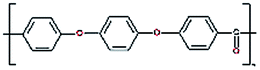
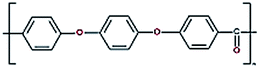
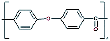
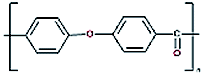
PEK HP3 powder supplied by EOS, Germany,22 PEEK 450PF and 150PF powder, both supplied by Victrex (UK), were used for laser sintering.23 PEK HP3 is the only commercialized powder designed for the laser sintering process. PEEK 150PF and 450PF are not specifically designed for the laser sintering system; in order to improve the powder flow, they were conditioned at 250 °C for 24 hours and sieved before manufacturing.24 PEEK 150PF and 450PF have the same molecular structure but different molecular weight, while PEK HP3 and PEK HT G22 differs in molecular structure. The glass transition temperature (Tg), melting temperature (Tm), molecular weight and molecular structure of the powders proposed for investigation are presented in Table 1. The material used for the manufacture of injection moulding samples is an Poly Ether Ketone (PEK) injection moulding grade, VICTREX HT G22 granules, equivalent to PEK HP3 powder.23| Powder | T g (°C) | T m (°C) | Molecular structure | M n (g mol−1) |
|---|---|---|---|---|
| PEEK 450PF | 147 | 343 |
|
32![[thin space (1/6-em)]](https://www.rsc.org/images/entities/char_2009.gif) 000 000 |
| PEEK 150PF | 147 | 343 |
|
23000 |
| PEK HP3 | 164 | 372 |
|
23000 |
| PEK HT G22 | 160 | 373 |
|
23000 |
Manufacturing
Characterization
In order to investigate the crystal morphology inside the fabricated samples, the specimens were fractured at room temperature and then the sputter coating machine was used to apply gold/palladium coating on the fracture surfaces to improve the electrical conductivity of the polymer and to obtain high resolution images. The setting of the coating thickness was 10 nm.
To explore in more detail the crystalline structure, PAEK samples were chemically etched and then imaged again with SEM. Two methods were used to prepare the etched samples.
Method 1: the cross sections of samples were manually polished by using wet SiC papers with various grits, staring from 800 grit, followed by 1200, 2000, 3000 and 5000 grits then finishing with a very fine 7000 grit SiC paper. After polishing, the permanganic chemical etching as proposed by Bassett et al. was applied by soaking the prepared samples into etching solution. To prepare the etching solution, 1 g of potassium permanganate (97%, Sigma-Aldrich, UK) was ground into fine powder with a mortar and pestle.17 Then the fine powder was added into 40 ml orthophosphoric acid (98%, Sigma-Aldrich, UK) and stirred for at 20 min to dissolve the powder. 10 ml distilled water was then added into the solution and stirred to mix. The polished samples were etched with the prepared solution in a glass baker in an ultrasonic bath for fifty minutes. The samples and etching solution were poured into 100 ml hydrogen peroxide (2% in water) to terminate the etching. Samples were washed several times with distilled water before SEM characterization.
Method 2: the fracture surfaces of PAEKs samples were directly etched in the solution without polishing. The same etching procedure as described above (method 1) was applied here. For the etched samples, the coating thickness was set to 5 nm.
Results
PAEKs powders
As demonstrated by the SEM images in Fig. 1, the PEEK and PEK powders with size in order of tens of microns are composed of clusters of small particles with sizes of the order of few microns. It is seen from the SEM images that these small particles contain submicron size fibrils, which are further confirmed by TEM as seen in Fig. 2.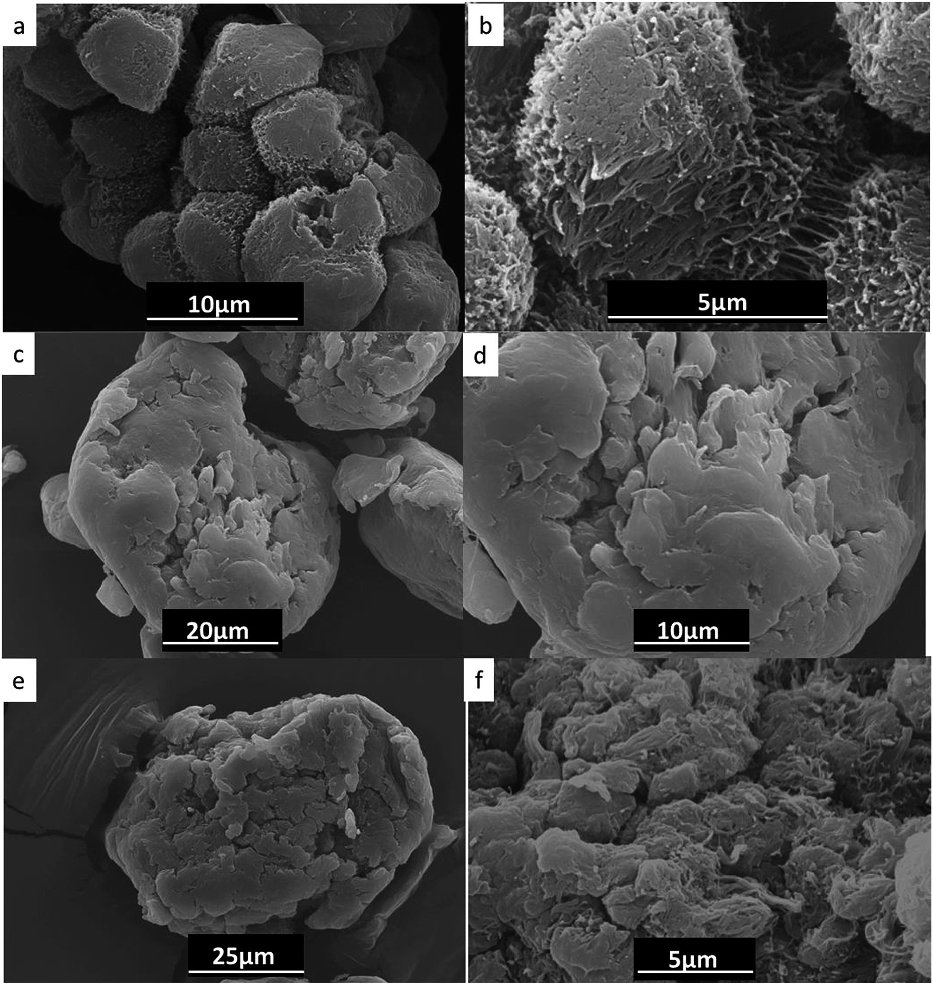 | ||
| Fig. 1 SEM microstructure of PAEK powders: PEEK 150PF (a) and (b), PEEK 450PF (c) and (d), and PEK HP3 (e) and (f). (a) and (c) and (e) are low magnification SEM images, showing the PAEK powders are composed of clusters of small particles with sizes of the order of few microns. (b), (d) and (f) are high magnification SEM images, showing the fibril structure of small particles in PAEK powder. | ||
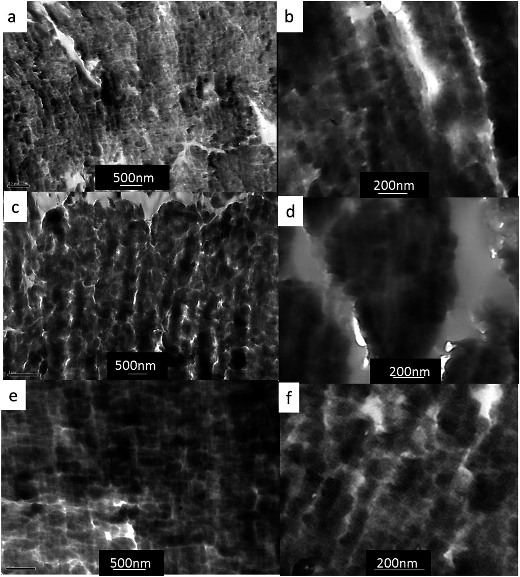 | ||
| Fig. 2 TEM microstructure of PAEKs powder: PEEK 150PF (a) and (b), PEEK 450PF (c) and (d), and PEK HP3 (e) and (f). (a) and (c) and (e) are low magnification images, showing that fibrils observed in the SEM images in Fig. 1 are orientated in a preferred direction. (b), (d) and (f) are high magnification images, showing the fibrils are actually made by arrays of connected granular blocks having size of several tens of nanometers. | ||
Low magnification images show that all fibrils are orientated in a preferred direction. Previous studies on polyolefins reported similar particles and fibril structures in polymer powder produced from chemical synthesis process.26,27 Interestingly, the fibrils in PAEKs powder are actually made by arrays of connected granular blocks having size of several tens of nanometers, as shown in the high magnification images in Fig. 2.
Laser sintered PAEKs
Fig. 3 shows TEM images of samples of various sintered PAEKs. In Fig. 3, all samples show spherulitic morphology which is the typical crystal morphology of crystalline PAEKs as reported in many other studies.13–15,17,28 The size of the spherulites appearing in all three types of laser sintered PAEKs is approximately 6 μm.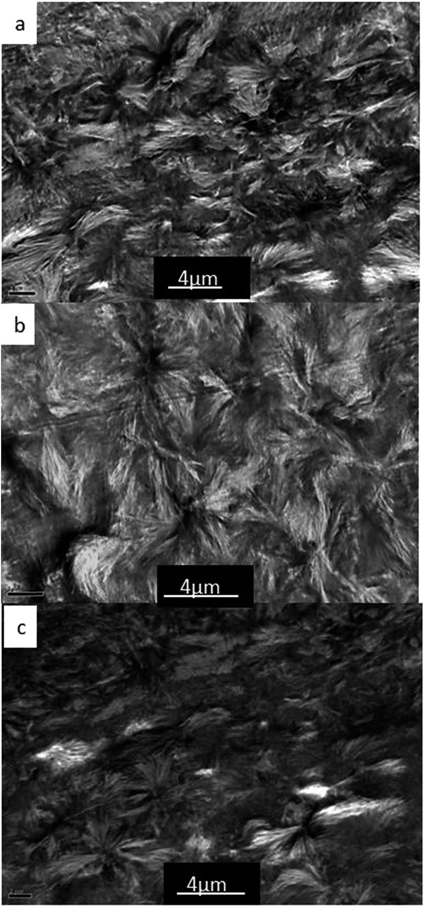 | ||
| Fig. 3 Spherulitic crystal structure in laser sintered samples PEEK 150PF (a), PEEK 450PF (b) and PEK HP3 (c). The size of spherulites appearing in all three types of laser sintered PAEKs is approximately 6 μm. | ||
The SEM images in Fig. 4 show the morphology of spherulites on the fracture surface of the three types of laser sintered PAEK samples. Surprisingly, rather than stacks of smooth lamellar spreading in radial directions as observed under TEM, numerous granular blocks appeared as part of the spherulite. These granular blocks are self-assembled into arrays following a spherulitic configuration. Moreover, closer comparison of the images in Fig. 4 (b), (d) and (f) indicates that these granular blocks assemble slightly differently within the formed spherulites. In the case of PEEK 150PF and PEK HP3, the granular blocks are assembled along the radial directions of the spherulite, while the granular blocks in PEEK 450PF are aligned in the radial as well as the circumferential directions in a spider web-like structure. Granular blocks in PEEK 150PF and PEK HP3 have sizes of approximately 120 nm and 145 nm, respectively. In PEEK 450PF, the granular blocks aligned in radial directions have sizes of approximately 120 nm, while those aligned in circumferential directions have sizes of approximately 75 nm.
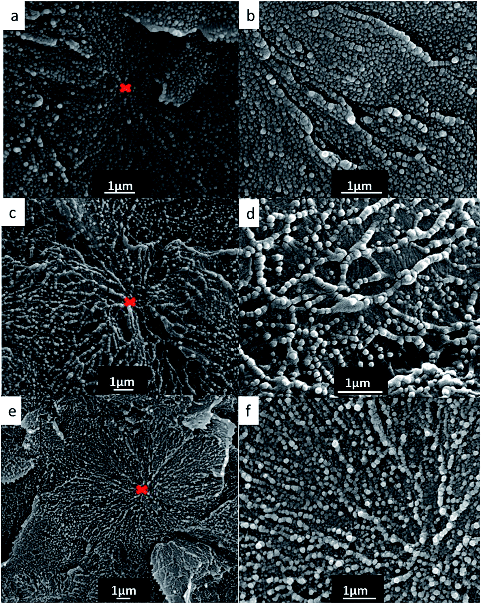 | ||
| Fig. 4 SEM images reveal the granular blocks in the spherulites crystals: PEEK 150PF (a) and (b), PEEK 450PF (c) and (d), and PEK (e) and (f). The centre of spherulite is marked with red crosses. Granular blocks appear as part of the spherulite, which are self-assembled into arrays following a spherulitic configuration. The granular blocks assemble slightly differently within the formed spherulites. In the case of PEEK 150PF (a) and (b) and PEK HP3 (e) and (f), the granular blocks are assembled along the radial direction of the spherulite, while the granular blocks PEEK 450PF (c), (d) are aligned in the radial as well as the circumferential direction in a spider web-like structure. | ||
In an attempt to confirm that the granular blocks are crystalline in structure, an amorphous PEEK sample was prepared for comparison. PEEK 150PF was selected for this purpose. The powder was dispersed on a glass slide and melted on a hot stage at 400 °C. The samples were then quenched immediately in water to obtain amorphous PEEK samples. The PEEK manufactured by this method was transparent. To confirm that the quenched PEEK is indeed amorphous material, the prepared sample was investigated by SEM, XRD and DSC. The PEEK 150PF powder and laser sintered samples were also analyzed using SEM, XRD and DSC and the results are compared in Fig. 5. No diffraction peaks were found in the XRD spectrum of amorphous PEEK, only the broad background peak was recorded. While diffraction peaks were found in both powdered and laser sintered samples. This shows the amorphous nature of the quenched PEEK sample. The DSC traces of the quenched PEEK are typical DSC traces of amorphous PEEK, as found in other studies.16,20,28 The enthalpy of the cold crystallization endothermic peak at 180 °C is equal to that of the exothermic melting peak at 345 °C which concludes that the quenched PEEK has zero initial crystallinity according to the equation,
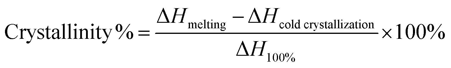
 | ||
| Fig. 5 (a) The SEM fracture surface image of quenched PEEK 150PF, (b) the XRD spectrum of quenched PEEK 150PF, (c) the DSC thermogram of the quenched PEEK 150PF, (d) the SEM image of PEEK 150PF powder, (e) the XRD spectrum of PEEK 150PF powder, (f) the DSC thermogram of the PEEK 150PF powder, (g) the SEM fracture surface image of laser sintered PEEK 150PF, (h) the XRD spectrum of laser sintered PEEK 150PF and (i) the DSC thermogram of the laser sintered PEEK 150PF. | ||
For comparison, the DSC traces of the initial PEEK 150PF powder and the laser sintered PEEK 150PF are given in Fig. 5(d) and (e). The DSC measurements suggest that both samples are semi-crystalline material. The laser sintered 150PF shows double melting peaks. The PEEK 150PF powder has a broad melting peak and the shape of the peak is non-symmetric which could suggest the presence of overlapped melting peaks. The DSC traces and crystallinity of powder and laser sintered PEEK 150PF samples are not exactly the same, as they had been experiencing different thermal histories due to their different manufacturing processes employed originally. Examples of DSC traces of laser sintered PEEK 450PF, PEK HP3 and injection moulded PEK HT G22 are shown in the ESI.†
In Fig. 5(a), the SEM image from the fracture surface of the quenched PEEK shows the absences of crystal blocks in the amorphous PEEK. The fracture surface is rather flat and micro-cracks induced by thermal shrinkage are the only visible microstructure features present in the amorphous sample. This result clearly demonstrates that the granular blocks identified in laser sintered samples are crystalline in structure. Hereinafter, the granular blocks identified in the laser sintered PAEKs are referred to as granular crystal blocks.
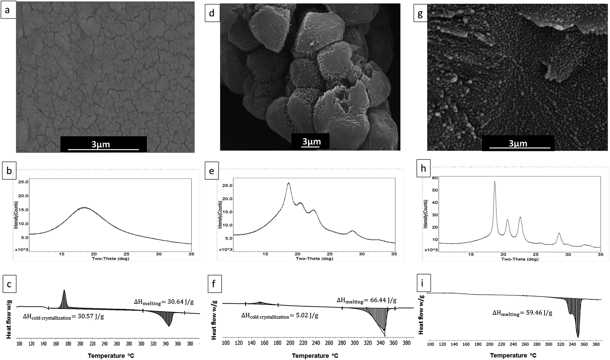
Chemical etching was applied in order to obtain a better understanding of the internal structure of the large granular crystal blocks.17 After etching, the large granular crystal blocks were no longer visible; they were split into small crystals of 20–30 nm in size, as shown in Fig. 6. Fig. 6(a)–(c) show the small crystals exposed on the polished cross section after etching (prepared by method 1), while (d)–(f) show the small crystals exposed on the etched fracture surface without polishing (prepared by method 2). As it can be seen, the polishing has no significant effect on the size of small crystals. Hereinafter, the small crystals identified on the etched surface are referred as primary crystals. This result suggests that each large granular crystal block is composed of several primary crystals and a secondary structure, present amongst the primary crystals. The secondary structure is likely to have a less-ordered structure such that they were preferentially removed during etching.
 | ||
| Fig. 6 SEM images showing the small primary crystals exposed on the etched surface of various samples. (a)–(c) show the primary crystals on polished cross section of PEEK 150PF, PEEK 450PF and PEK HP3, respectively. (d)–(f) show the primary crystals on the etched fracture surface without polishing. The secondary structures presented between primary crystals are removed away by etching. | ||
Discussion
From these results it was concluded that laser sintered PEEK and PEK have a hierarchical structure including three types of crystal morphologies within the spherulites:(i) Primary crystal blocks having size of 20–30 nm.
(ii) Secondary structure, less ordered than primary crystal and bonding primary crystals together.
(iii) Granular crystal blocks, which are composed of primary crystal blocks and secondary structures 75–145 nm size.
Scheme 1 schematically illustrates the proposed relationship between these morphologies. It is possible that the secondary structure provides strong enough bonding among the primary crystals such that internal fracture of large granular crystal blocks would not take place; the fracture only occurring along the boundaries of large granular crystal blocks. Therefore, the crystals revealed on the fracture surfaces are the large granular crystal blocks rather than small primary crystals.
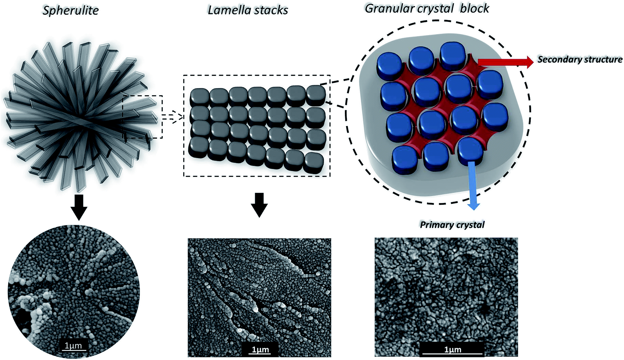 | ||
| Scheme 1 Schematic illustration of the proposed hierarchical spherulitic crystal structure of PAEKs. | ||
It is not clear why these structures are visible in the SEM but cannot be detected during TEM imaging. Upon a general review of crystal structures in semi-crystalline polymers, it is found that many other researchers were not able to detect the granular crystal blocks under TEM either; they only detected the lamellar structure of the spherulites.13,14,16,17 This could be explained by the different image formation method of these two techniques. The SEM scanning electron images are produced by the morphology and surface topography, while the TEM bright field images are attributed to the mass thickness and diffraction contrast. The granular crystals exposed to surface may be easily identified by their unique morphological features in the SEM. However, in the TEM there is no significant mass thickness or diffraction contrast between crystal blocks as they are composed of the same material.
AFM has also been used as an alternative method to study the crystal morphology in the literature. The lamellar structure of semi-crystalline polymer PP, PP copolymer, LDPE and PMMA have been widely studied with AFM.29–33 Strobl et al. identified a nodular crystal structure in the lamellae of PP and LDPE. Strobl's study found that the size of the nodular crystals was approximately 20 nm.29,30 Based on these findings, Strobl et al. suggested that the crystal growth involved multiple steps. Formation of the nodular crystals is the first step of crystallization. Then, the nodular crystals merge into lamellae and ultimately transform into the final crystal form.29,30 In our study, the high resolution SEM investigation suggests that there are two types of nodular crystals present in the PAEKs, the small primary crystal and the large granular crystal block.
AFM analysis was performed here to further demonstrate the presence of granular crystal blocks and primary crystals in PAEK observed by SEM. The AFM analysis was carried out on the surface of isothermally crystallized PEEK 150PF film. Neither the laser sintered sample nor the injection moulded specimen prepared in this study are ideal samples for AFM analysis. For example, the laser sintered sample was fully embedded in the powder bed during laser sintering which left a loss powder layer on top of the surface. Since the surface of injection moulded sample was in contact with the mould, any machining pattern on the mold surface could be copied onto the polymer surface. All of these surface imperfections could mask the true crystal morphology of polymer during AFM scanning. Therefore, the PEEK 150PF film prepared by isothermal crystallization was chosen as an ideal sample for AFM study.
Fig. 7(a) and (b) show the AFM images obtained from the as-prepared melt crystalized PEEK 150PF film (no etching applied prior to AFM scanning). As can be seen, the AFM images again suggest the presence of the nodular crystals. Both large crystal blocks in (a) and the small primary crystals in (b) can be detected by AFM. Fig. 7(c) and (d) show the linear profiles across the nodular crystals marked with the dotted lines in the AFM images. The sizes of crystals were measured from the peak width. When scanning a relatively large area, the large granular crystals with sizes of approximately 40–50 nm were detected by AFM as shown in Fig. 7(a) and (c).
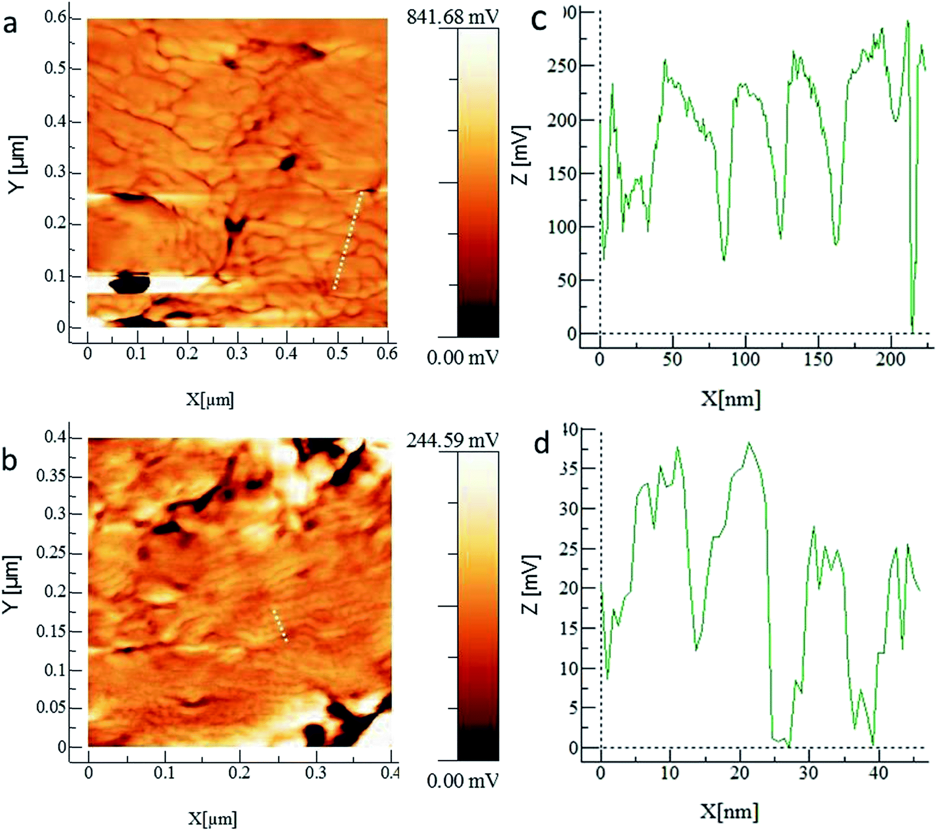 | ||
| Fig. 7 AFM images taken from the melt crystalized PEEK 150PF. (a) and (b) show the large granular crystals and small primary crystals, respectively. (c) and (d) are the surface profiles of nodular crystals measured from the dotted lines marked in (a) and (b), respectively. | ||
Samples from the same isothermal crystallized PEEK 150PF film were also used for SEM investigation. Fig. 8 shows the SEM images of spherulitic crystalline structure and confirmed again the presence of granular crystal blocks as previously noticed in the laser sintered samples as shown in Fig. 4, although this time, the structure was created through isothermal crystallization. The size of crystal blocks of the isothermal crystallized PEEK 150PF is approximately 55 nm. The size of small primary crystal measured from SEM images of etched film sample is approximately 15 nm. The size of crystal blocks and primary granular crystals is similar as the ones observed in AFM Fig. 7(a) and (b), respectively. The size measured from SEM images is slightly larger than the one measured by AFM. It could that the gold/palladium coating on the SEM samples leads to the overestimation of crystal size. Upon scanning a fairly small region, much smaller primary crystals were resolved with sizes of approximately 8–10 nm as shown in Fig. 7(b) and (d).
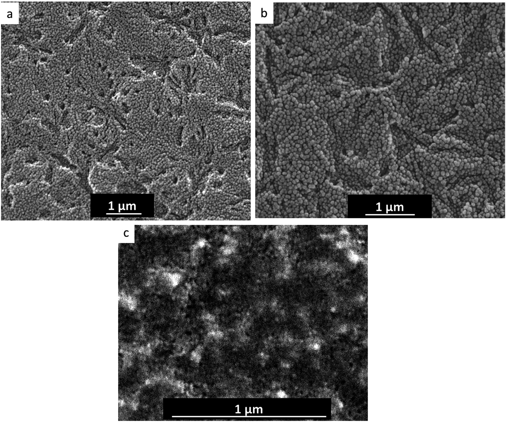 | ||
| Fig. 8 The crystal morphology of melt crystallized PEEK 150PF, imaged with SEM. (a) is the low magnification image showing the spherulitic crystalline structure and the granular crystal blocks. (b) is a high magnification image showing the granular crystal blocks in detail. (c) is the high magnification images taken from etched sample showing small primary crystals. | ||
Fig. 4 and 8 show that the hierarchical crystal structure is formed independent of the processing method, although their size and configuration of assembly could be influenced by the grade of material and processing history. To further prove this finding, the crystal morphology of injection moulded PEK specimens was studied. Fig. 9 shows that the granular crystal blocks appear on the fracture surface of injection moulded specimens as well with the size of approximately 200 nm. The size of small primary crystal measured from SEM images of etched injection moulded sample is approximately 12 nm.
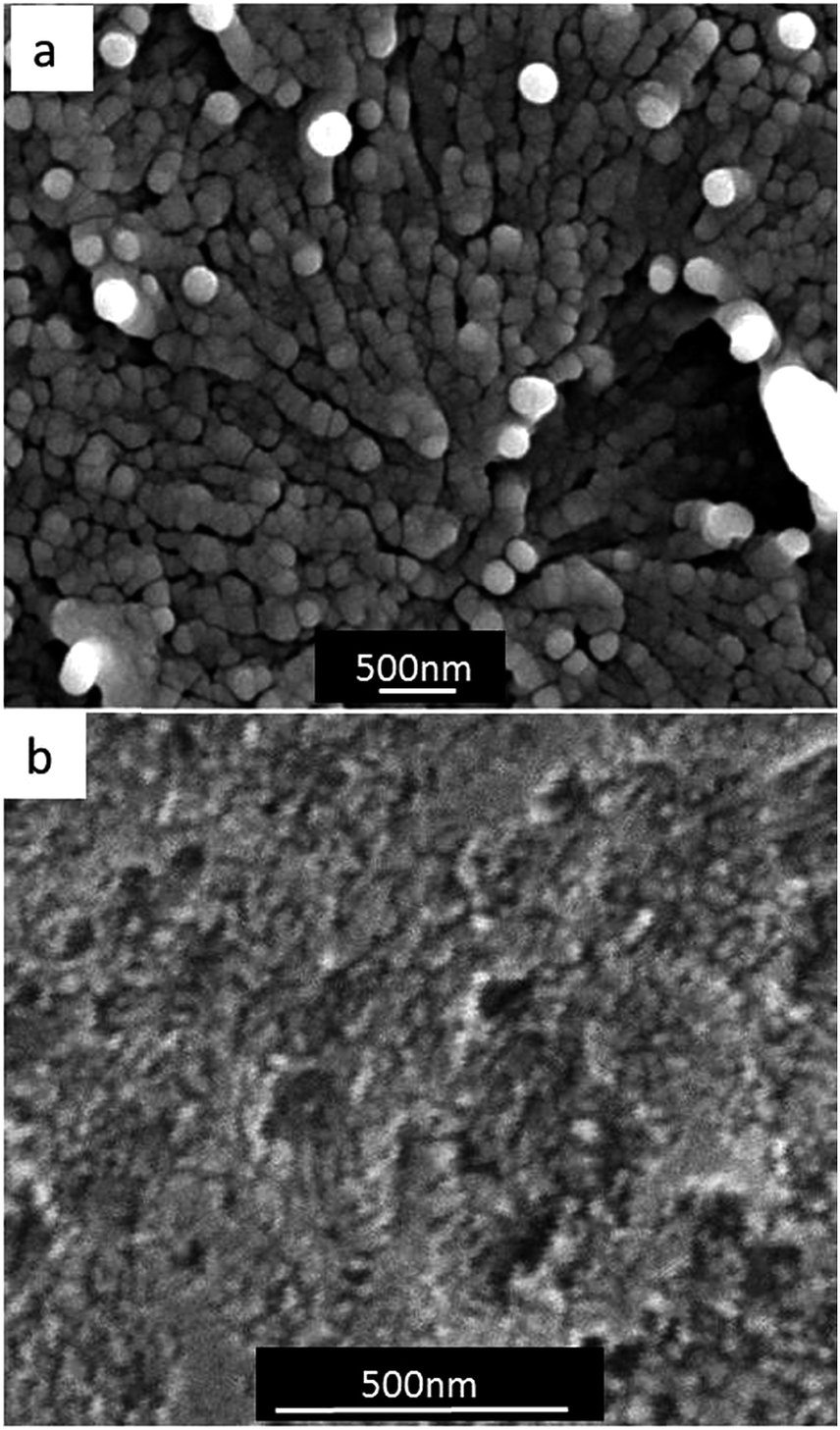 | ||
| Fig. 9 The crystal morphology of injection moulded PEK HT G22 imaged with SEM (a) shows the large crystal blocks (b) shows the small primary crystals after chemical etching. | ||
In the literature, the lamellar thickness of PEEK prepared with conventional isothermal crystallization method was found to be 6–10 nm by SAXS measurements, depending on the crystallization temperature and time.14,18–20,28 According to the AFM measurements carried out in this study, the size of the primary crystals (8–10 nm) in isothermally crystallized sample is similar to the lamellar thickness of PEEK reported in the literature with samples made by a melt crystallization process. This suggests that the primary crystals could be involved in the lamellae formation in PEEK. The size of the primary crystals in laser sintered PAEKs (20–30 nm) is larger than that found in isothermal melt crystallized samples but still of the same order of magnitude. Further investigation is needed to achieve a better understanding of the effect of processing method and thermal history on the crystal size.
Conclusions
The crystal morphology of three grades of PAEKs was investigated from powder to manufactured samples. The individual powder is composed of small particles which are built from clusters of oriented fibrils. The fibrils contain primary crystals of approximately 40 nm in size. This study identified a new hierarchical spherulitic structure for PAEKs composed of small primary crystal blocks, secondary structures and large granular crystal blocks; the latter being the assembly of the first two structures. These crystal morphologies were found in laser sintered, injection moulded and isothermally crystallized samples by SEM and AFM studies. The primary crystal in the laser sintered samples is approximately 20–30 nm in size, and is the smallest crystal structure found in PAEKs spherulites under the SEM observation. In the injection moulded and melt crystallized samples, the primary crystals have the size of approximately 10–15 nm. The configuration of assembly and the size of the large granular crystal blocks are material dependent.Acknowledgements
This work is supported by the UK Engineering and Physical Science Research Council (EPSRC grant no EP/L017318/1 – Particle Shape and Flow behaviour in Laser Sintering: from modelling to experimental validation). The authors would like to thanks Mr Richard Davies (Centre for Additive Layer Manufacturing, University of Exeter) for expertise and help on manufacturing the laser sintered polymer and Dr Peter Splatt (College of Biosciences, University of Exeter) for his support on TEM sample preparation.Notes and references
- T. E. Attwood, P. C. Dawson, J. L. Freeman, L. R. J. Hoy, J. B. Rose and P. A. Staniland, Polymer, 1981, 22(8), 1096–1103 CrossRef CAS.
- S. M. Kurtz and J. N. Devine, Biomaterials, 2007, 28(32), 4845–4869 CrossRef CAS PubMed.
- D. P. Jones, D. C. Leach and D. R. Moore, Polymer, 1985, 26(9), 1385–1393 CrossRef CAS.
- J. Altmeyer, J. F. dos Santos and S. T. Amancio-Filho, Mater. Des., 2014, 60, 164–176 CrossRef CAS.
- S.-L. Gao and J.-K. Kim, Composites, Part A, 2000, 31(6), 517–530 CrossRef.
- B. S. Tripathy and M. J. Furey, Wear, 1993, 162–164 Search PubMed , Part A, (0), 385–396.
- A. M. Díez-Pascual, M. Naffakh, J. M. González-Domínguez, A. Ansón, Y. Martínez-Rubi, M. T. Martínez, B. Simard and M. A. Gómez, Carbon, 2010, 48(12), 3500–3511 CrossRef.
- K. Bassett, R. Carriveau and S. K. D. Ting, Sustainable Energy Technologies and Assessments, 2015, 11, 186–193 CrossRef.
- D. G. LeGrand, Annealing in Encyclopedia of Polymer Science and Technology, John Wiley & Sons, Inc, 2002 Search PubMed.
- A. R. McLauchlin, O. R. Ghita and L. Savage, J. Mater. Process. Technol., 2014, 214(1), 75–80 CrossRef CAS.
- O. Ghita, E. James, R. Davies, S. Berretta, B. Singh, S. Flint and K. E. Evans, Mater. Des., 2014, 61, 124–132 CrossRef CAS.
- O. R. Ghita, E. James, R. Trimble and K. E. Evans, J. Mater. Process. Technol., 2014, 214(4), 969–978 CrossRef CAS.
- A. J. Waddon, M. J. Hill, A. Keller and D. J. Blundell, J. Mater. Sci., 1987, 22(5), 1773–1784 CrossRef CAS.
- L. Jin, J. Ball, T. Bremner and H.-J. Sue, Polymer, 2014, 55(20), 5255–5265 CrossRef CAS.
- J.-N. Chu and J. Schultz, J. Mater. Sci., 1990, 25(8), 3746–3752 CrossRef CAS.
- D. C. Bassett, R. H. Olley and I. A. M. Al Raheil, Polymer, 1988, 29(10), 1745–1754 CrossRef CAS.
- R. H. Olley, D. C. Bassett and D. J. Blundell, Polymer, 1986, 27(3), 344–348 CrossRef CAS.
- B. S. Hsiao, K. H. Gardner, D. Q. Wu and B. Chu, Polymer, 1993, 34(19), 3996–4003 CrossRef CAS.
- B. S. Hsiao, K. H. Gardner, D. Q. Wu and B. Chu, Polymer, 1993, 34(19), 3986–3995 CrossRef CAS.
- D. J. Blundell, Polymer, 1987, 28(13), 2248–2251 CrossRef CAS.
- Y. Lee and R. S. Porter, Macromolecules, 1987, 20(6), 1336–1341 CrossRef CAS.
- EOS, http://www.eos.info/en/home.html.
- Victrex, http://www.victrex.com.
- F. Müller, A. Pfister and M. Leuterer, PAEK powder, in particular for the use in a method for a layer-wise manufacturing of a three-dimensional object, as well as method for producing it, Google Patents, 2012 Search PubMed.
- M. Leuterer, et al., Influencing specific mechanical properties of three-dimensional objects manufactured by a selective sintering by means of electromagnetic radiation from a powder comprising at least one polymer or copolymer, Google Patents, 2013 Search PubMed.
- M. Kakugo, H. Sadatoshi, J. Sakai and M. Yokoyama, Macromolecules, 1989, 22(7), 3172–3177 CrossRef CAS.
- T. F. L. McKenna, A. Di Martino, G. Weickert and J. B. P. Soares, Macromol. React. Eng., 2010, 4(1), 40–64 CrossRef CAS.
- D. J. Blundell and B. N. Osborn, Polymer, 1983, 24(8), 953–958 CrossRef CAS.
- T. Hugel, G. Strobl and R. Thomann, Acta Polym., 1999, 50(5–6), 214–217 CrossRef CAS.
- G. Strobl and T. Y. Cho, Eur. Phys. J. E, 2007, 23(1), 55–65 CrossRef CAS PubMed.
- Y. K. Godovsky and S. N. Magonov, Langmuir, 2000, 16(7), 3549–3552 CrossRef CAS.
- J. K. Hobbs, Polymer, 2006, 47(15), 5566–5573 CrossRef CAS.
- C. De Rosa, F. Auriemma, R. Di Girolamo and O. R. de Ballesteros, J. Polym. Sci., Part B: Polym. Phys., 2014, 52(10), 677–699 CrossRef.
Footnote |
| † Electronic supplementary information (ESI) available. See DOI: 10.1039/c5ra17110e |
| This journal is © The Royal Society of Chemistry 2016 |