Sun Hwa Parka,
Hyun Min Parka,
Sang Soo Hanb,
Sang Yun Hanc and
Jae Yong Song*a
aMaterials Genome Center, Korea Research Institute of Standards and Science (KRISS), Daejeon 305-340, Republic of Korea. E-mail: jysong@kriss.re.kr
bCenter for Computational Science, Korea Institute of Science and Technology (KIST), Seoul 136-791, Republic of Korea
cDept. of Nanochemistry, Gachon University, Gyeonggi 461-701, Republic of Korea
First published on 23rd December 2015
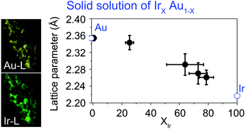
A solid solution alloy of Ir–Au has been theoretically predicted to be an excellent catalyst for dissociating hydrogen, equivalent to Pt. However, Ir and Au atoms are known to be thermodynamically immiscible. In this work, we show that the thermodynamics of the Ir and Au binary system can be changed by nanoscale effects and that electrochemically synthesized Ir–Au alloys have a solid-solution structure with a wide range of compositions. This work is expected to open up the potential synthesis of new catalytic materials.
In this work, we have synthesized solid solution alloys of Ir–Au in a wide range of compositions using a facile, cost-effective, and one-step electrochemical deposition without any surfactants, organic materials or supported oxides. We demonstrate that Ir and Au can be miscible at atomic levels and form solid-solution alloys, confirmed by analyses of crystal structure.
Nanostructured Ir–Au alloys were electrochemically deposited on Au-coated Si substrates using an electrochemical system (Modulab, Solartron). For this three-electrode system, a Pt wire (0.5 mm in diameter and 1 m in length, Sigma Aldrich) and a KCl-saturated Ag/AgCl electrode were used as a counter electrode and a reference, respectively. A sputtered Au film (90 nm in thickness) on a Si wafer was used as a working electrode with an exposed area of 0.5 cm × 0.5 cm. The aqueous electrolyte was composed of 25 μM IrCl3·nH2O and 12.5 μM HAuCl4·nH2O at 323 K. The reverse-pulse potentiodynamic process was performed at a reduction potential (VR) of 10 V and oxidation potential (VO) of 0 V for 24 h (see Fig. S1†).
As shown in Fig. 1(a), Ir–Au alloys with a columnar structure were uniformly deposited as a layer of 80 nm thickness. The morphologies and crystal structures were investigated by field-emission scanning electron microscope (SEM, Hitachi S-4800), energy dispersive X-ray spectroscopy detector (EDS, EDAX Inc.), Cs-corrected scanning transmission electron microscope (TEM, JEOL JEM-ARM200F, 200 kV), and X-ray diffractometers (XRD, Cu-K, Bruker D8, θ–2θ scan). The X-ray diffraction angles were calibrated by using Si powder (NIST SRM 640c) which was simultaneously measured as an internal standard (2θ = 47.304°) (see Fig. S2†).
![]() | ||
Fig. 1 Top-view and cross-sectional SEM images of Ir–Au alloys grown on Au-coated substrate by electrochemical-deposition. |
The XRD peaks shown in Fig. 2(a) and (b) indicate that the nanostructured Ir–Au alloys have two broad diffraction peaks (blue line) around 2θ of 39.8° and 85.7°, respectively, as indicated by solid circles. The two diffraction peaks are not identified in the JCPDS card of Ir and Au phases (#46-1044 and #04-0784, respectively). The former peak falls between 38.185 to 41.661°, 2θ angles corresponding to the (111) planes of Au and Ir, respectively, while the latter peak exists between 81.721 to 88.055°, 2θ angles corresponding to the (222) planes of Au and Ir, respectively.
![]() | ||
Fig. 2 XRD patterns (blue) of Ir–Au alloys grown on Au-coated Si substrate in the 2θ range (°) of (a) 37 to 43 and (b) 82 to 88 selected in Fig. S2.† (the green line denotes the XRD pattern of Au-coated Si substrate). |
Recently, a theoretical prediction suggested that the XRD pattern of an Ir50Au50 solid solution would be similar to that of pure Pt because it has a face centered cubic (FCC) structure and a lattice parameter very close to that of the Pt phase.1 Therefore, we detached Ir–Au alloys deposits from the substrate and analysed the crystal structure using the BFTEM image and the selected area electron diffraction pattern of them (Fig. S3†). The d-spacings of the diffraction pattern are not identical to those of pure Ir and Au phases. They exist between the d-spacings of Ir and Au, rather close to those of the Pt phase (see Fig. S4†). Therefore, the electron diffraction pattern of the Ir–Au alloy shown in Fig. S3† might be indexed to be (111), (200), (220), (311) and (222) planes, from inner ring to outer ring, following the JCPDS card of Pt (#04-0802).
For minute observation of the crystal structure of the Ir–Au alloys, the cross-sectional structure between the Ir–Au alloys and Au-coated substrate was systematically investigated by high-resolution TEM (HRTEM) images and fast Fourier transformed (FFT) images, as shown in Fig. 3. For the marked positions of (i) to (v) in the cross-sectional bright-field TEM (BFTEM) image of Fig. 3(a), the corresponding HRTEM and FFT images show that the Ir–Au alloys grew in the [111]-direction (the red circles in FFT images denote the (111) plane). This is in agreement with the XRD result of the (111) preferred orientation shown in Fig. 2 (also see Fig. S2†). In Fig. 3(b)-(iv), the multiple twins are denoted by yellow dotted lines. It is presumed that the twins might be formed by energy minimization because the increasing Ir content in the alloy increase the misfit strain energy of the nanostructured alloys.15
Fig. 4(a) shows the EDS results for Ir–Au binary alloys with various compositions corresponding to the marked position (i) to (v) along the thickness direction. At the position (i), only the Au peak was observed due to Au film as a substrate, as shown in Fig. 4(a)-(i). The Ir peak started to appear at the (ii) position and the intensity of the Ir peak increased along the thickness direction of the Ir–Au alloys, as shown in Fig. 4(a).
![]() | ||
Fig. 4 (a) EDS spectra of the marked positions corresponding to (i) to (v) shown in Fig. 3(a) and (b) variation of lattice parameter with the Ir composition following Vegard's law. |
For comparison, pure Ir and Au layers were synthesized by the same electrochemical deposition process (see Fig. S5†). The pure Ir layer was composed of particulate grains with a size less than 10 nm, whereas pure Au comprised larger grains with a size over 300 nm.
During the initial growth of the Ir–Au alloys, Au ions would be primarily reduced due to identical atomic radius and chemical affinity. In consecutive deposition, the reduction of Ir ions favorably occurred to form the Ir–Au alloy phase owing to the smaller atomic radius of Ir (the atomic radii of Ir and Au are 1.35 and 1.44 Å, respectively).
Fig. 4(b) shows that the lattice parameter of the Ir–Au alloys decreased with the increase in Ir content in the alloys. It is noted that the lattice parameter changed more or less linearly with the variation of Ir content, following Vegard's law.16 The Ir–Au alloys had the face-centered cubic structure shown in Fig. 3, and the lattice parameters varied between those of the Au and Ir phases. This indicates that the Ir and Au atoms are miscible, forming a solid solution of Ir and Au at the nanoscale structure, violating the understanding that Ir and Au are immiscible in bulk phase.
The nanoscale growth of Ir–Au alloys might be related to the field-enhanced electrochemical driving force in an ultra-dilute electrolyte.13,14 As a parallel study, electrodeposition was conducted on stainless steel substrate in the mixed electrolytes with various concentrations of IrCl3·nH2O and HAuCl4·nH2O (see Fig. S6†). When the electrolyte concentration was increased to 5 mM IrCl3·nH2O and 0.1 mM HAuCl4·nH2O, the deposits were separated as two phases, i.e., Ir and Au phases, as confirmed by XRD and EDS analyses (see Fig. S6(a)-(i), (b)-(i) and (c)-(i)†). In the higher concentration electrolyte (5 mM IrCl3·nH2O and 0.1 mM HAuCl4·nH2O), the lower reduction potential (5 V) was used due to the higher electrolyte conductivity, otherwise the electrodeposition was not possible due to severe evolution of H2 gas at the higher reduction potential of 10 V. However, the same electrodeposition condition (VR = 10 V and VO = 0 V, 25 μM IrCl3·nH2O and 12.5 μM HAuCl4·nH2O) on stainless steel substrate led to the formation of Ir–Au alloys, as shown in Fig. S6(a)-(ii) and (b)-(ii).† Despite the existence of Ir and Au elements confirmed by the EDS (Fig. S6(c)-(ii)†), a new XRD peak appeared between 38.185 to 41.661°, 2θ angles corresponding to the (111) planes of Au and Ir, respectively, in an agreement with the results shown in Fig. 2(a). This peak is supposed to correspond to the (111) plane of Ir–Au alloy with a FCC crystal structure, which was suggested by the theoretical study.1 For comparison, when the constant voltage of 1 V, i.e., lower electric field, was applied in the same ultra-dilute electrolyte (25 μM IrCl3·nH2O and 12.5 μM HAuCl4·nH2O), the only Au phase was deposited (see Fig. S6(a)-(iii), (b)-(iii) and (c)-(iii)†). Therefore, the nanoscale growth of Ir–Au alloys is believed to be driven by the enhanced electric field in an ultra-dilute electrolyte.
In summary, the nanoscale solid solution synthesis of Ir–Au binary alloys was demonstrated using a simple, cost-effective, and one-step electrochemical-deposition. The present result demonstrates the realization of an Ir–Au alloy that may have excellent catalytic properties, equivalent to Pt, as predicted by the recent theoretical calculation. Further studies on the catalytic properties of the Ir–Au alloys are needed to evaluate them as a catalyst for replacing Pt nanocrystals. The nanoscale synthesis of Ir–Au solid solution is expected to contribute to the potential synthesis of new alloy materials system which are presently considered to be immiscible in bulk.
Footnote |
† Electronic supplementary information (ESI) available: Additional results on variation of current density with time in reverse-pulse potentiodynamic mode, d-spacings and microstructural analysis. See DOI: 10.1039/c5ra26472c |
This journal is © The Royal Society of Chemistry 2016 |