
 Open Access Article
 This Open Access Article is licensed under a Creative Commons Attribution-Non Commercial 3.0 Unported Licence
Resistive pressure sensors based on freestanding membranes of gold nanoparticles†
Hendrik
Schlicke
,
Matthias
Rebber
,
Svenja
Kunze
and
Tobias
Vossmeyer
*
Institute of Physical Chemistry, University of Hamburg, Grindelallee 117, 20146 Hamburg, Germany. E-mail: tobias.vossmeyer@chemie.uni-hamburg.de; Fax: +49 40 42838 3452; Tel: +49 40 42838 7069
First published on 30th November 2015
Abstract
In this communication the application of gold nanoparticle membranes as ambient pressure sensors with electromechanical signal transduction is demonstrated. The devices were fabricated by sealing microstructured cavities with membranes of 1,6-hexanedithiol cross-linked gold nanoparticles, which were electrically contacted by metal electrodes deposited on both sides of the cavities. Variations of the external pressure resulted in a deflection of the membranes and, thus, increased the average interparticle distances. Therefore, the pressure change could easily be detected by simply monitoring the resistance of the membranes.
Due to their tunable electronic, mechanical and optical properties, freestanding membranes of gold nanoparticles (GNPs) capped with monofunctional ligands, interlinked with bi- or multifunctional molecular cross-linkers or embedded in polymer matrices are promising candidates for the application as functional materials in micro- and nanoelectromechanical systems (MEMS/NEMS). In contrast to conventional silicon based MEMS/NEMS requiring elaborate multi-step lithographic fabrication schemes, noble metal nanoparticle composites can be fabricated and deposited by cost-effective procedures such as spin-coating, ink-jet printing,1,2 stamping3 and are compatible with a broad variety of rigid or flexible substrate materials.
Recently, a series of MEMS/NEMS applications was demonstrated by several research groups. Kanjanaboos et al. demonstrated the fabrication of microscale drumhead resonators from freestanding monolayers of monothiol-capped GNPs with resonance frequencies in the MHz range.4 Tsukruk and coworkers reported the fabrication of Golay type IR microimagers based on nanocomposite GNP/polymer membranes deposited on microcavities.5 The group also presented the application of freestanding membranes of polymer-encapsulated GNPs as pressure gauges.6 However, optical readout techniques of the membrane deflection were applied in all cases. More recently, we reported on the first electrostatic actuator based on a freestanding membrane of alkanedithiol (ADT) cross-linked GNPs.7
GNP membranes cross-linked using dithiols offer the ability to adjust the conductivity over several orders of magnitude.8,9 Using shorter-chain ADTs, fairly good conductivities can be achieved. Analogously to thin films of monothiol-capped GNPs deposited on flexible substrates,10 the charge transport through assemblies of ADT cross-linked GNPs is sensitive to strain, directly affecting the interparticle distances and impeding tunnel currents. Based on this behavior, the applicability of substrate supported dithiol cross-linked GNP films as sensitive strain gauges with gauge factors Gs of 10–20 was demonstrated.11,12
Previously, freestanding membranes of highly ordered GNP monolayers were fabricated and their remarkable elastic properties were probed by AFM indentation measurements.13,14 Si et al. reported the fabrication of freestanding monolayer sheets from Au@Ag nanocubes, which could be lithographically milled into nanoribbons or folded into 3d origami.15 In a recent study16 we reported on the fabrication of freestanding 1,9-nonanedithiol (9DT) cross-linked GNP membranes on circular apertures (∼100 μm diameter) and the characterization of their viscoelastic properties by AFM micro-bulge tests.17 The Young's modulus was measured in the low GPa range and it was demonstrated that these membranes withstand pressure loadings of several kPa, corresponding to a biaxial stress of tens of MPa.16 These mechanical properties together with their electric conductivity make crosslinked gold nanoparticle membranes interesting functional materials for MEMS/NEMS applications.
In this communication we present the fabrication of resistive pressure gauges employing a 1,6-hexanedithiol (6DT) cross-linked GNP membrane as strain sensitive transducer. To the best of our knowledge, this is the first report on sensors utilizing the unique electromechanical properties of a freestanding nanoparticle membrane to enable a direct and simple resistive signal readout.
For fabricating the sensor devices, GNP membranes were deposited onto 3d microstructures featuring rectangular cavities, typically of ∼40 μm in width and ∼500 μm in length. The microstructures were prepared from SU-8, a negative tone photoresist commonly used for the fabrication of MEMS structures,18,19 using standard photolithography on thermally oxidized silicon wafers (oxide thickness 300 nm). The depth of the cavities (∼40 μm) could be trimmed by varying the resist layer thickness. In proximity to the long sides of the cavities, gold or platinum electrodes (∼40 nm thickness) were deposited for measuring the resistance of the freestanding membrane sections. A schematic showing the device architechture is presented in Fig. 1a. Fig. 1b shows a SEM image of the microcavity prepared in SU-8 resist with proximal metal electrodes, before depositing the nanoparticle membrane. A detailed description of the microstructure fabrication process is provided in the ESI.†
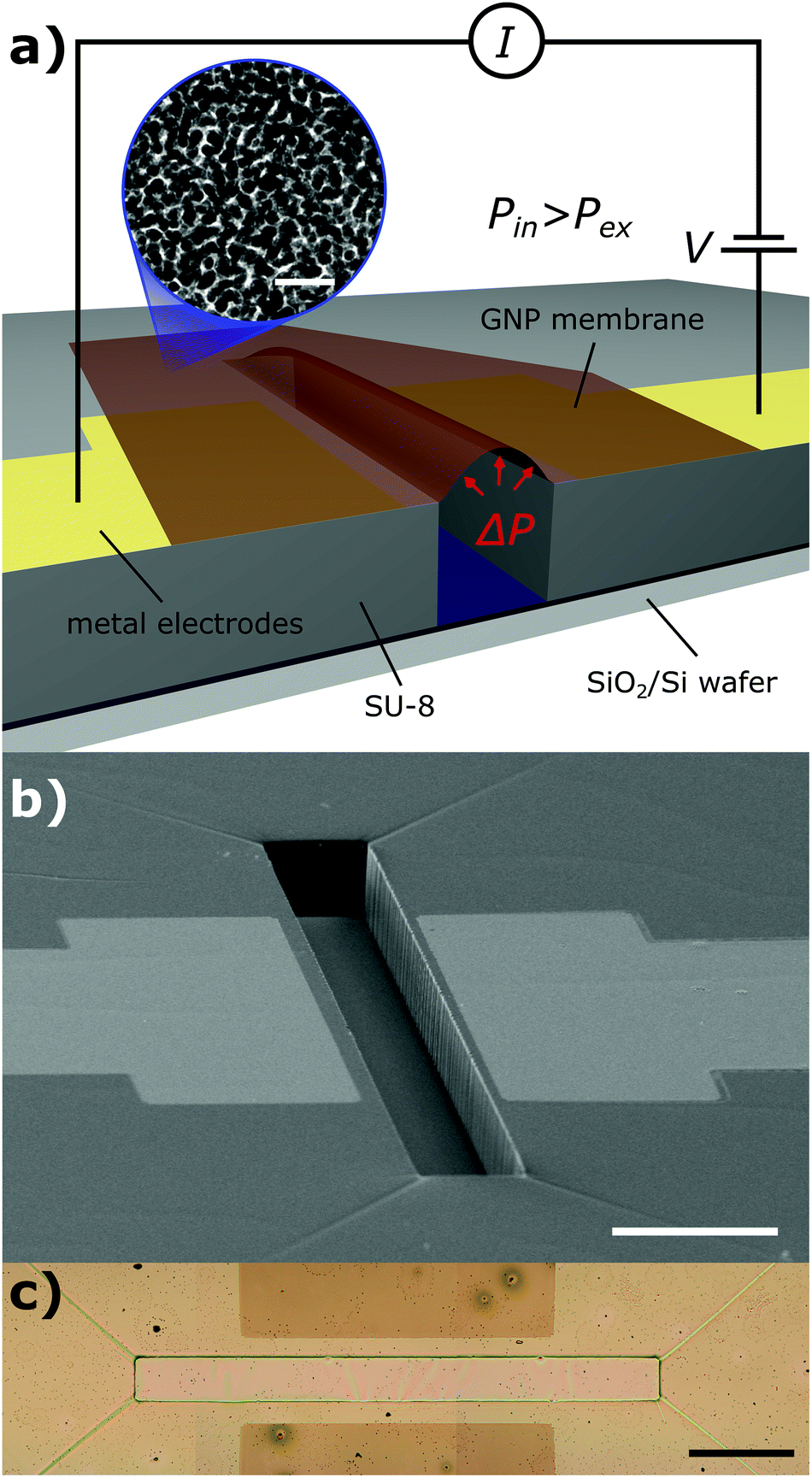 | ||
| Fig. 1 (a) Schematic showing a cross-sectional view of a GNP membrane based pressure sensor. The GNP membrane is sealing the cavity microstructured into SU-8 photoresist. Electrodes deposited onto the SU-8 layer are used to monitor the membrane's resistance under applied pressure loading. The inset shows a TEM image of a 1,6-hexanedithiol cross-linked GNP membrane (scale bar: 25 nm). (b) SEM image of a microcavity with proximal metal electrodes prior to membrane deposition. Scale bar: 100 μm. (c) Optical micrograph of a 6DT cross-linked GNP membrane deposited onto a 3d electrode microstructure. Scale bar: 100 μm. | ||
6DT cross-linked GNP membranes were fabricated by spin-coating a heptanoic solution of GNPs (diameter (3.5 ± 0.7) nm) and a methanolic solution of 6DT alternatingly onto a glass substrate, as reported earlier.20 The resulting GNP films showed a typical conductivity of around 0.1 S cm−1.7 Thicknesses of the films were measured by atomic force microscopy (AFM).20 A TEM image revealing the granular structure of the 6DT cross-linked GNP membrane is shown as inset in Fig. 1a. See the ESI† for a representative absorbance spectrum, a current–voltage (I–V) measurement, and an AFM scan of the substrate supported GNP film used for device fabrication.
Following deposition, the cross-linked GNP films were transferred from their initial substrates by floating them on demineralized water.20 After an incubation period of up to two days at ambient conditions, the membranes could easily be lifted off their glass substrates by carefully immersing the latter into water. Doing this, the membranes detached from the substrates and remained floating at the liquid–air interface. Subsequently, the electrode microstructures were used to skim the membranes from the water surface. While the samples were allowed to dry, the membranes settled to the 3d structures and remained freestanding over the rectangular cavities. The substrates were then fixed onto custom-designed printed circuit boards, contacted and transferred to a custom-built pressure cell. A Keithley 2601A source measure unit was employed to source a constant voltage of 1 V across the device and to measure the resulting current. The pressure cell was equipped with a cascade of valves, suitable for applying pressure transients in a range of ±10 kPa, relative to ambient pressure. As reference sensor a digital pressure gauge (Sensortechnics HDIM100DBF8P5) was connected to the cell. Details of the setup can be found in the ESI.†
Fig. 1c shows the optical micrograph of a device with a 6DT cross-linked GNP membrane (55 nm thickness) spanning the rectangular microfabricated cavity. Also the gold electrodes (∼300 μm width, ∼80 μm distance), covered by the membrane are clearly recognized. An initial resistance of 259 kΩ was determined for this device, corresponding to a sheet resistance of Rs = 0.95 MΩ. Compared to conventional metal foil strain gauges the significantly higher resistance of GNP based transducers allows for operating the devices under lower power dissipation.10 Additionally, it is straightforward to adjust the sheet resistance for specific device requirements because the resistivity of cross-linked GNP films can be tuned over several orders of magnitude by varying the size8,9,20 and structure21 of the cross-linker.
The application of positive pressure transients of up to 8 kPa resulted in pressure differences between the cavity and the exterior, causing an inward deflection of the freestanding membrane. Movements of the membrane could clearly be observed using a microscope camera (Fig. 2a, middle). A movie showing the periodical deflections of the nanoparticle membrane induced by the repeated pressure loadings shown in Fig. 2b can be found in the ESI.† The deflection of the membrane was accompanied by an increase in resistance as shown by the response transients in Fig. 2b. When negative external pressures of up to −8 kPa (relative to ambient) were applied again pressure differences between the cavity and the exterior were established. In this case the freestanding membrane showed outward deflections while remaining attached to the SU-8 layer surrounding the cavity (Fig. 2a, right). As expected, the device responded with a similar increase in resistance (up to ∼0.7%) for positive and negative applied pressures (see Fig. 2b), especially in the higher pressure range, resulting from similar strain experienced by the membrane in both cases, inward and outward deflection. It is to note that the device remained functional over the course of the study of several weeks.
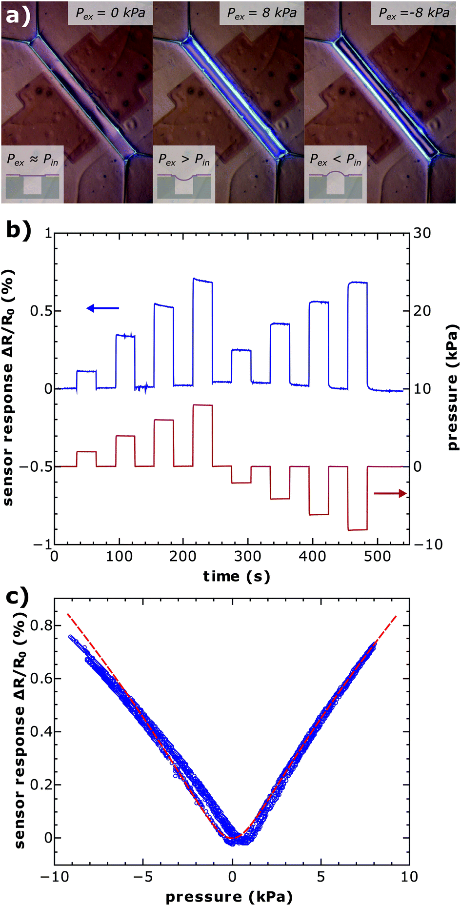 | ||
| Fig. 2 (a) Optical micrographs of a pressure gauge fabricated from a 6DT cross-linked GNP membrane placed in a pressure cell under an external pressure loading of (left) 0 kPa, (center) 8 kPa and (right) −8 kPa (relative to the ambient pressure). The deflections of the membrane inwards and outwards the rectangular microcavity are observable by the reflections of the non-centered incident microscope illumination on opposite sides of the bulge. (b) Pressure transients (0 to ±8 kPa) applied to the device (red) and resulting resistance changes relative to the baseline resistance R0 (blue). (c) Transfer function of the device relating the applied external pressure to the measured resistance change. An estimate of the transfer function, which is based on the membrane's mechanical properties, the dimensions and geometry of the device, and a gauge factor Gs of 7, is depicted as dashed red line. Details to the underlying calculation are provided in the ESI.† | ||
Fig. 2c shows the sensor's transfer curves obtained by repeatedly sweeping the external pressure and continuously monitoring the current at an applied voltage of 1 V. Corresponding resistance and pressure time series can be found in the ESI.† The sensor displayed an almost linear response for the positive and negative external pressure branch. A slight offset of the response curve's minimum is observed and is attributed to a slight difference between the initial cavity pressure and the ambient pressure.
The response of the pressure sensor was estimated by taking into account the mechanical properties of 6DT cross-linked GNP membranes obtained by AFM bulge tests (ESI†).7 Using this data and the device geometry, an estimate of the bulge height of the membrane in response to the applied pressure loading as well as the resulting strain could be calculated. Taking into account a constant gauge factor Gs of 7 and a residual membrane stress of 6 MPa (values in the MPa range are common for freestanding GNP membranes7,16), resulted in estimates of the sensor responses which are, within the given pressure range of ±8 kPa, very similar to the experimental data. This is clearly seen in Fig. 2c, which shows the calculated transfer function (dashed red line) in very good agreement with the experimental response curve. A detailed description of the calculation as well as simulations regarding the influences of different device parameters on the sensor's response characteristics are provided in the ESI.†
In summary, we presented the first prototype of a resistive pressure sensor based on a freestanding membrane of gold nanoparticles. A sensor response of up to ∼0.7% was obtained for pressure changes in a range of ±8 kPa. The measured sensor responses were found in good agreement with a simple approximate model relating the applied external pressures to the membrane strain, and assuming a gauge factor Gs of 7, similar as observed for substrate supported strain gauges based on 9DT cross-linked GNP coatings.11 According to previous findings reported for strain gauges based on GNP assemblies, it should be possible to enhance the sensitivity of the presented pressure sensor by the following adjustments: first, it was demonstrated that the resistive strain sensitivity of substrate-supported GNP films increased with decreasing thickness and was highest for monolayer films. This finding was attributed to the 2d confinement of conduction paths in the case of the monolayer film.22 Additionally, as shown by our model calculation provided in the ESI,† decreasing the membrane thickness increases the device's sensitivity because thinner membranes are bulged more heavily than thicker ones at a given pressure. Second, an increase of the nanoparticle size is assumed to increase the sensitivity, because the gauge factor of nanoparticle based resistive strain gauges scales with the particle diameter, as deduced from a simple geometric model.10 Third, the order of the particles in a freestanding membrane is expected to influence the strain sensitivity. Compared to a highly ordered GNP membrane a disordered membrane responds to stress more easily by local rearrangements, microcrack formation and local relaxation rather than by homogeneous changes in the interparticle distances.23 Taken together, ultimate sensitivities should be achievable by employing membranes consisting of a single, highly ordered monolayer of relatively large GNPs. This, however, will require reducing the device's dimensions in order to avoid collapse of the membrane and to enable electrode aspect ratios allowing for practical resistance measurements. Additionally, we note that by applying a more elaborate capacitive readout of the membrane deflection, it should be possible to determine the direction of the pressure variation with respect to the internal cavity pressure.
Acknowledgements
The work of H. S. is supported by a scholarship of the Joachim Herz Foundation. T. V. acknowledges financial support by the German Research Foundation (DFG), grant number VO698/3-1. Furthermore we thank Stefan Werner for transmission electron microscopy measurements.References
- S. Fuller, E. Wilhelm and J. Jacobson, J. Microelectromech. Syst., 2002, 11, 54–60 CrossRef.
- E. S. Park, Y. Chen, T.-J. K. Liu and V. Subramanian, Nano Lett., 2013, 13, 5355–5360 CrossRef CAS PubMed.
- B. Kowalczyk, M. M. Apodaca, H. Nakanishi, S. K. Smoukov and B. a. Grzybowski, Small, 2009, 5, 1970–1973 CrossRef CAS PubMed.
- P. Kanjanaboos, X.-M. Lin, J. E. Sader, S. M. Rupich, H. M. Jaeger and J. R. Guest, Nano Lett., 2013, 13, 2158–2162 CrossRef CAS PubMed.
- C. Jiang, M. E. McConney, S. Singamaneni, E. Merrick, Y. Chen, J. Zhao, L. Zhang and V. V. Tsukruk, Chem. Mater., 2006, 18, 2632–2634 CrossRef CAS.
- C. Jiang, S. Markutsya, Y. Pikus and V. V. Tsukruk, Nat. Mater., 2004, 3, 721–728 CrossRef CAS PubMed.
- H. Schlicke, D. Battista, S. Kunze, C. J. Schröter, M. Eich and T. Vossmeyer, ACS Appl. Mater. Interfaces, 2015, 7, 15123–15128 CAS.
- Y. Joseph, I. Besnard, M. Rosenberger, B. Guse, H.-G. Nothofer, J. M. Wessels, U. Wild, A. Knop-Gericke, D. Su, R. Schlögl, A. Yasuda and T. Vossmeyer, J. Phys. Chem. B, 2003, 107, 7406–7413 CrossRef CAS.
- M. Brust, D. J. Schiffrin, D. Bethell and C. J. Kiely, Adv. Mater., 1995, 7, 795–797 CrossRef CAS.
- J. Herrmann, K. H. Müller, T. Reda, G. R. Baxter, B. Raguse, G. J. J. B. De Groot, R. Chai, M. Roberts and L. Wieczorek, Appl. Phys. Lett., 2007, 91, 183105 CrossRef.
- T. Vossmeyer, C. Stolte, M. Ijeh, A. Kornowski and H. Weller, Adv. Funct. Mater., 2008, 18, 1611–1616 CrossRef CAS.
- M. Segev-Bar and H. Haick, ACS Nano, 2013, 7, 8366–8378 CrossRef CAS PubMed.
- W. Cheng, M. J. Campolongo, J. J. Cha, S. J. Tan, C. C. Umbach, D. A. Muller and D. Luo, Nat. Mater., 2009, 8, 519–525 CrossRef CAS PubMed.
- K. E. Mueggenburg, X.-M. Lin, R. H. Goldsmith and H. M. Jaeger, Nat. Mater., 2007, 6, 656–660 CrossRef CAS PubMed.
- K. J. Si, D. Sikdar, Y. Chen, F. Eftekhari, Z. Xu, Y. Tang, W. Xiong, P. Guo, S. Zhang, Y. Lu, Q. Bao, W. Zhu, M. Premaratne and W. Cheng, ACS Nano, 2014, 8, 11086–11093 CrossRef CAS PubMed.
- H. Schlicke, E. W. Leib, A. Petrov, J. H. Schröder and T. Vossmeyer, J. Phys. Chem. C, 2014, 118, 4386–4395 CAS.
- A. Turchanin, A. Beyer, C. T. Nottbohm, X. Zhang, R. Stosch, A. Sologubenko, J. Mayer, P. Hinze, T. Weimann and A. Gölzhäuser, Adv. Mater., 2009, 21, 1233–1237 CrossRef CAS.
- E. H. Conradie and D. F. Moore, J. Micromech. Microeng., 2002, 12, 368–374 CrossRef CAS.
- H. Lorenz, M. Despont, N. Fahrni, N. LaBianca, P. Renaud and P. Vettiger, J. Micromech. Microeng., 1997, 7, 121–124 CrossRef CAS.
- H. Schlicke, J. H. Schröder, M. Trebbin, A. Petrov, M. Ijeh, H. Weller and T. Vossmeyer, Nanotechnology, 2011, 22, 305303 CrossRef PubMed.
- J. M. Wessels, H.-G. Nothofer, W. E. Ford, F. von Wrochem, F. Scholz, T. Vossmeyer, A. Schroedter, H. Weller and A. Yasuda, J. Am. Chem. Soc., 2004, 126, 3349–3356 CrossRef CAS PubMed.
- C. Farcau, H. Moreira, B. Viallet, J. Grisolia, D. Ciuculescu-Pradines, C. Amiens and L. Ressier, J. Phys. Chem. C, 2011, 115, 14494–14499 CAS.
- N. Olichwer, E. W. Leib, A. H. Halfar, A. Petrov and T. Vossmeyer, ACS Appl. Mater. Interfaces, 2012, 4, 6151–6161 CAS.
Footnote |
| † Electronic supplementary information (ESI) available. See DOI: 10.1039/c5nr06937h |
| This journal is © The Royal Society of Chemistry 2016 |