
Substrate tolerant direct block copolymer nanolithography†
Tao
Li
a,
Zhongli
Wang
ab,
Lars
Schulte
ab and
Sokol
Ndoni
*ab
aDepartment of Micro- and Nanotechnology, Technical University of Denmark, DK-2800 Kgs. Lyngby, Denmark. E-mail: sond@nanotech.dtu.dk
bCenter for Nanostructured Graphene (CNG), Technical University of Denmark, DK-2800 Kgs. Lyngby, Denmark
First published on 13th November 2015
Abstract
Block copolymer (BC) self-assembly constitutes a powerful platform for nanolithography. However, there is a need for a general approach to BC lithography that critically considers all the steps from substrate preparation to the final pattern transfer. We present a procedure that significantly simplifies the main stream BC lithography process, showing a broad substrate tolerance and allowing for efficient pattern transfer over wafer scale. PDMS-rich poly(styrene-b-dimethylsiloxane) (PS-b-PDMS) copolymers are directly applied on substrates including polymers, silicon and graphene. A single oxygen plasma treatment enables formation of the oxidized PDMS hard mask, PS block removal and polymer or graphene substrate patterning.
The ever growing demand for increased device functionality, higher data processing speed and larger data storage density drives the searching for new technology to fabricate electronic components with smaller dimensions. BC lithography is a promising platform to meet the key challenges of small feature size with high resolution and high throughput at low cost.1,2 The domain size can be controlled in the range of 5–50 nm by controlling the molecular weight of the BC and the segregation strength between the blocks in the synthesis step. Several morphologies including spheres, lamellae and cylinders have been explored for nanolithography application.3 BCs combining high intrinsic immiscibility (quantified by a high Flory–Huggins interaction parameter χ) with high etching contrast are extremely attractive as precursors for nanolithographic masks.4 PS-b-PDMS (SD) has χSD ∼ 0.27 at room T, and can easily self-assemble into morphologies with sub-10 nm features.5,6 Under oxygen plasma the PDMS block is oxidized to hard and thermally stable silicon oxycarbide, which acts as the effective lithographic mask, while the PS block is efficiently degraded.7 These two features have gained SD intense research interest in the last decade. However, the orientation control of SD is notoriously challenging due to the large surface energy mismatch between the blocks.8 As a result a top wetting layer of PDMS preferably forms at the SD–air interface. A brush layer is routinely applied to prevent dewetting and a top-coat or sophisticated annealing conditions9 are used for orientation control.
The present contribution is motivated by the great interest in SD for nanolithography, with a focus on even more challenging and rarely reported PDMS-rich BCs, which are equally, if not more, important for the pattern transfer process.10 The BC film is applied directly on the substrate, thus bypassing the step of initial substrate surface modification found in nearly all the reports in the field. The preliminary surface modification, including the grafting of a neutral polymer brush layer onto the substrate,11 is the result of presuming thin film BC stability and self-assembly in terms of equilibrium. Uneven BC swelling under selective solvent vapor is known to shift the morphology by changing the effective volume fraction,12,13 which opens up the process window for capturing the targeted morphology kinetically. The lithography process is schematically illustrated in Scheme 1 and proved valid for a number of substrates with widely varying surface energies. To the best of our knowledge, this is the first report on highly ordered PDMS-rich BC masks with perpendicular cylindrical orientation, which shows unparalleled simplicity and applicability in block copolymer nanolithography.
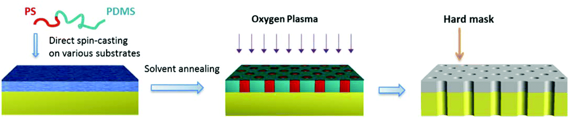 | ||
| Scheme 1 Schematic workflow of direct BC nanolithography: SDs in heptane are directly cast on various substrates including PS, polylactide (PLA), poly(methyl methacrylate) (PMMA), polysulfone (PSF), cross-linked 1,2-polybutadiene (PB), graphene and silicon. | ||
Four SDs with different number-average molecular weights (Mn) from 23.4 to 67.0 kg mol−1 are investigated (Table S1, ESI†). The PS volume fraction is in the range of 24–30%, which is within the typical composition range for cylinder bulk morphology (Fig. S1, ESI†). SD23, SD34 and SD42 are synthesized in our lab by living anionic polymerization14 with a narrow polydispersity index (PDI ≤ 1.03), and SD67 is purchased with somewhat higher PDI (1.45). SD solutions in heptane are spin-cast into sub-20 nm thin films on silicon and a number of common polymer substrates. Heptane is a nonsolvent for these polymer substrates, allowing direct spin-casting of the SD without any disturbance. Fig. 1a–c show the top view scanning electron microscopy (SEM) images of SD23, SD34 and SD42 after annealing. A well-ordered hexagonally packed cylinder morphology with narrow PS-cylinder size distribution is clearly seen, which can be visualized directly in SEM. A SEM image of SD67 after annealing (Fig. S2, ESI†) shows the same morphology but lacking in lateral order, which might be due to its large PDI. Compared with the morphology of the as-cast films or of films after thermal annealing (Fig. S3a and b, ESI†), it is evident that solvent annealing is effective on directing the SD self-assembly over large areas (2 inch wafer tested) with micrometer grain size (Fig. S3c†). The corresponding period (Table S1†) scales with the 0.6th power of BC molecular weights. A wide range of pore sizes from 13 nm (SD23) to 30 nm (SD67) is obtained. General shortcomings of solvent vapor annealing, including dewetting and deformation of the structures,15 are not observed in this study due to the limited PS chain mobility in the presence of a nonsolvent. The morphology is further confirmed by atomic force microscopy (AFM) (Fig. S4, ESI†).
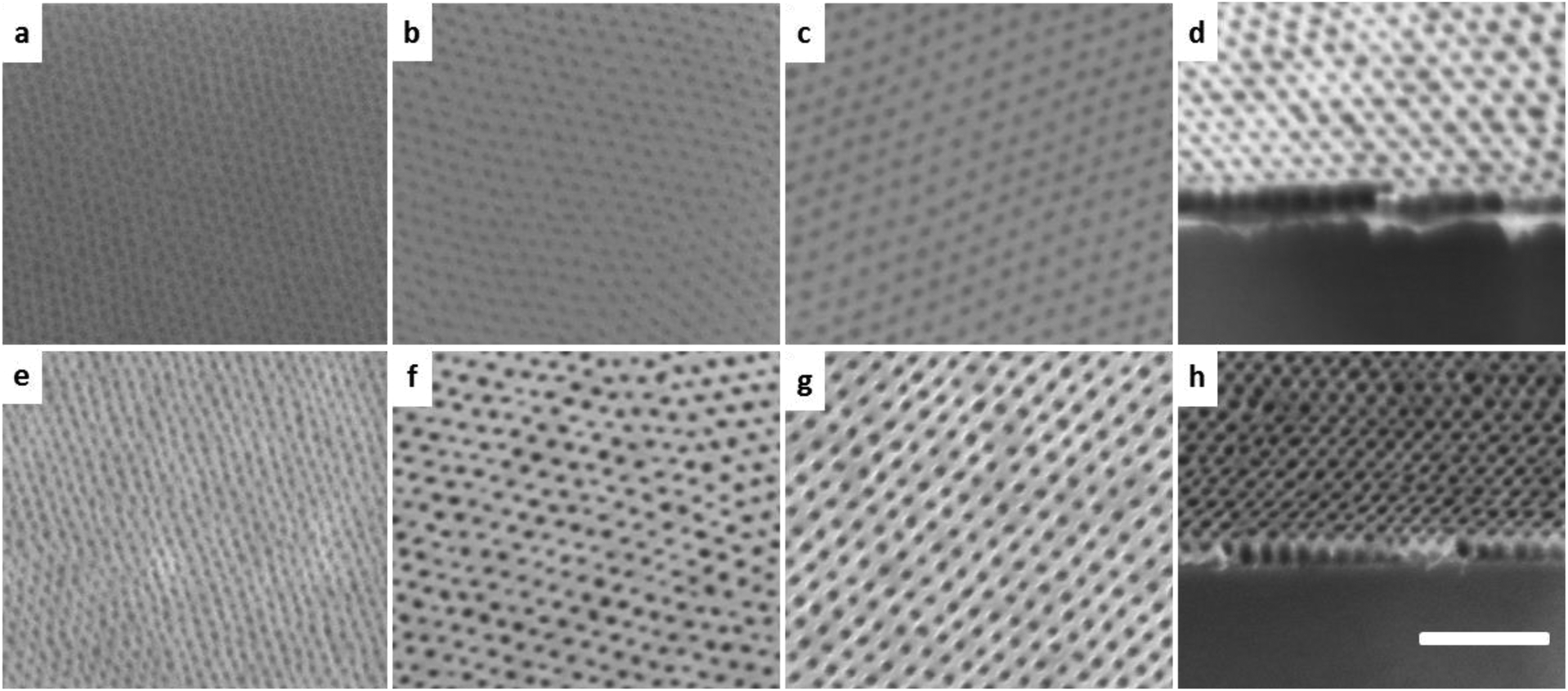 | ||
| Fig. 1 (a–c) Top view SEM images of the masks on PS after annealing: (a) SD23 annealed in 2,2,4-trimethylpentane (TMPA) for 40 minutes, (b) SD34 annealed in 2,4,4-trimethyl-1-pentene (TMPE) for 30 minutes, and (c) SD42 annealed in hexane for 40 minutes. (e–g) Top view SEM images of the masks on PS after pattern transfer: (e) SD23 and (f) SD34 after SF6 and O2 plasma etching, and (g) SD42 after O2 plasma etching alone. The O2 reactive ion etching (RIE) step solidifies the PDMS domain, removes the PS domain and transfers the pattern to the PS substrate simultaneously. (d and h) Tilted SEM images of the SD42 mask: (d) after etching and (h) after mask removal. All the samples are spin-cast on a PS 50k substrate coated on silicon wafer with a thickness of around 50 nm. Scale bar: 200 nm. | ||
The pattern transfer is conducted by RIE (Fig. 1e–g). In most cases, a short SF6 RIE is firstly used to remove a thin layer of residual PDMS on top. The improved SEM image contrast after etching suggests the successful pattern transfer, which is further evidenced by the cross-section image of the samples after etching (Fig. 1d and h). The mask can be readily removed by a SF6 RIE (confirmed by the absence of Si element in X-ray photoelectron spectroscopy measurement) without damage to the polymer substrate (Fig. 1h). Fig. S5 (ESI†) shows the SD23 only treated with O2 RIE and most of the pores stay clogged. However, in some cases (Table S2, ESI†), only an O2 RIE is sufficient to complete the pattern transfer (Fig. 1g). In these cases the film is free of a PDMS top wetting layer after solvent vapor annealing, which is difficult to obtain for PDMS-containing BC. The mask produced has high etching resistance under oxygen plasma and high thermal stability (the morphology stays the same after 700 °C for one hour).
A discussion of the annealing conditions, the time evolution of the structural order and a conjectured mechanism of pattern formation at optimum and post-optimum annealing conditions can be found in the ESI (Scheme S1 and Fig. S7†).
The presented approach also shows strong substrate independence, as demonstrated in Fig. 2 and 3. The observed self-assembly behavior is similar to the already discussed behavior on the PS substrate for all the tested substrates: PLA, PMMA, PSF, PB, graphene and silicon with a native oxide layer (the surface energy of these substrates can be characterized by water contact angle measurement summarized in Table S3†). The timing of the morphology evolution is somewhat different in each case but generally faster than the already discussed PS substrate. The pattern transfer is proved successful for all the substrates. Fig. 2b shows the cross-section of polysulfone patterned by the SD34 mask; a well-ordered nano-pore channel array is clearly observed. Polysulfone is a technologically relevant material for ultrafiltration membranes due to its high thermal, mechanical and chemical resistance.16 For membrane bio-analysis and separation, challenges still exist for producing reliable membranes with anti-fouling properties, high flux and narrow pore distribution. After oxygen plasma etching, the iso-porous PSF membrane becomes hydrophilic (water contact angle: 19°), which may significantly improve its anti-fouling properties.17,18 The demonstrated pattern transfer could offer an alternative solution to manufacture high performance thin polymer membranes.
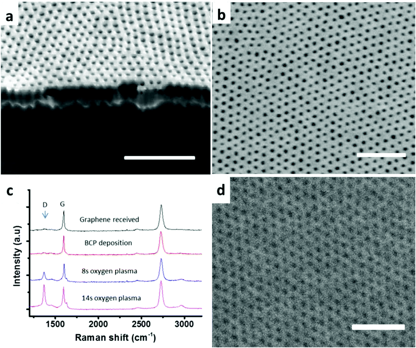 | ||
| Fig. 2 SEM images of pattern transfer to polysulfone and graphene. (a) Tilted and (b) top views of polysulfone patterned by SD34. (c) Raman spectrum characterization of graphene patterning in the presence of the mask from SD42 and (d) top-view SEM image of the graphene nanomesh patterned by SD42. Scale bars: 200 nm. | ||
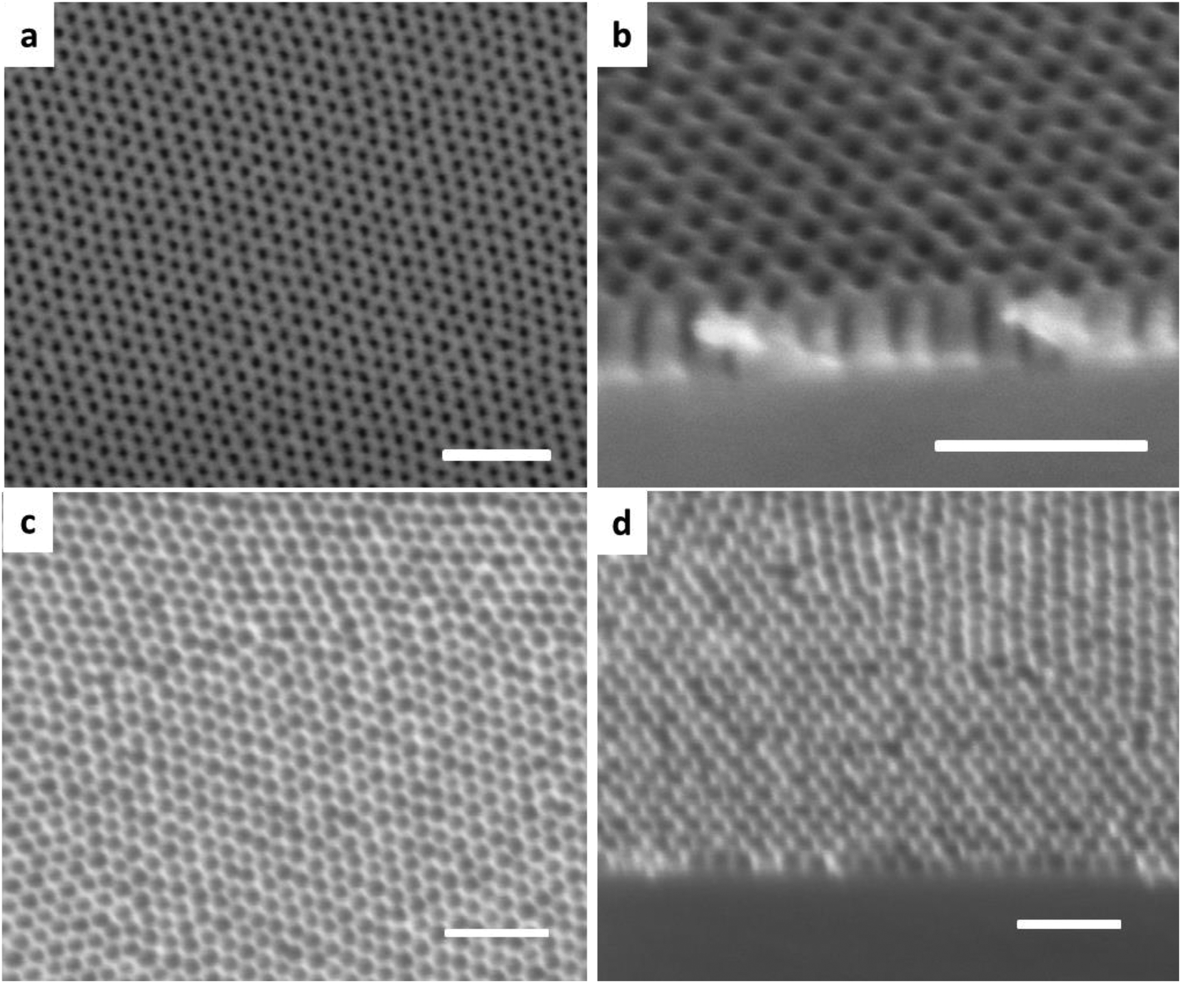 | ||
| Fig. 3 SEM image of (a) top-view and (b) cross-section of the silicon patterned by chlorine RIE. Holes with an aspect ratio exceeding 4 are clearly visible in (b). (c) Top-view and (d) cross-section of the silicon patterned by SF6 plasma etching. Several fluorine based RIE recipes including the Bosch process have been tested. Scale bars: 200 nm. | ||
This method is also particularly suitable for patterning two-dimensional materials where part of the single atom layer is removed in a controlled way to give tunable properties. Graphene nanomesh is a typical example, in which high-density arrays of nanoscale holes are punched.19 The available BC lithography for the graphene nanomesh is tedious, involving multiple deposition and etching steps.20 Most of all, it is difficult to reach sub-30 nm periods with the low-χ PS-PMMA mask used in most reports. Here, SD is directly deposited on CVD-grown single layer graphene. Fig. S6 (ESI†) shows a large-area mask covering the graphene without defects after solvent annealing. The pattern is well adjusted on graphene grain boundaries, multi-layer islands and other substrate defects. We use Raman spectroscopy to analyze the hole punching process. After the BC deposition, the spectrum stays the same. Increase in oxygen plasma etching time results in the increase of the D peak, which typically characterizes the hole enlarging process. The excellent process control is evidenced by the essentially unchanged width of the G peak. Fig. 2d shows the patterned graphene after removing a part of the mask by using a Scotch tape; the image shows a high fidelity reproduction of the mask morphology. The obtained graphene nanomesh has potentially many important applications, including the fabrication of field-effect transistors,21 gas sensors,22 and atomic-layer separation membranes.23
The oxidized PDMS masks can be used not only for patterning carbonaceous materials by oxygen RIE; they also show higher resistance over silicon under chlorine RIE as demonstrated by the SEM images shown in Fig. 3a and b. Unlike the isotropic fluorine plasma etching, where the pore-broadening is significant (see Fig. 3c and d), the silicon etching by chlorine plasma is highly anisotropic.24 Therefore, regular arrays of high-aspect-ratio holes in silicon are obtained by direct application of chlorine plasma to the oxidized PDMS mask. This process can be applied to pattern silicon with other morphologies, such as lines and dots by PDMS-based BC masks, which is of great relevance for the semiconductor industry and solid-state nanoporous materials.25
In conclusion, we have demonstrated a novel design for BC thin film morphology control, which significantly simplifies the nanolithography pattern transfer process on polymer substrates, graphene and silicon, opening up avenues for numerous potential applications. This conceptual approach provides a powerful toolset to obtain the desired BC mask morphologies, which are difficult to realize by conventional methods.
Author contributions
T. L. conceived and designed the experiments. T. L., Z. W. and L. S. performed the experiments. T. L. and S. N. analyzed the data. L. S. synthesized and characterized the block copolymers. T. L. and S. N. co-wrote the paper. S. N. supervised the project. All the authors discussed the results and corrected the manuscript. All authors have given their approval to the final version of the manuscript.Acknowledgements
This work was supported by the Center for Nanostructured Graphene sponsored by the Danish National Research Foundation, Project DNRF58, and by the Dept. of Micro and Nanotechnology at the Technical University of Denmark.References
- C. M. Bates, M. J. Maher, D. W. Janes, C. J. Ellison and C. G. Willson, Macromolecules, 2014, 47, 2–12 CrossRef CAS.
- J. Bang, U. Jeong, D. Y. Ryu, T. P. Russell and C. J. Hawker, Adv. Mater., 2009, 21, 4769–4792 CrossRef CAS PubMed.
- X. D. Gu, I. Gunkel and T. P. Russell, Philos. Trans. R. Soc. London, Ser. A, 2013, 371, 20120306 CrossRef PubMed.
- A. Nunns, J. Gwyther and I. Manners, Polymer, 2013, 54, 1269–1284 CrossRef CAS.
- Y. S. Jung and C. A. Ross, Nano Lett., 2007, 7, 2046–2050 CrossRef CAS PubMed.
- T. Nose, Polymer, 1995, 36, 2243–2248 CrossRef CAS.
- K. Fukukawa, L. Zhu, P. Gopalan, M. Ueda and S. Yang, Macromolecules, 2005, 38, 263–270 CrossRef CAS.
- E. Kim, W. Kim, K. H. Lee, C. A. Ross and J. G. Son, Adv. Funct. Mater., 2014, 24, 6981–6988 CrossRef CAS.
- K. W. Gotrik, A. F. Hannon, J. G. Son, B. Keller, A. Alexander-Katz and C. A. Ross, ACS Nano, 2012, 6, 8052–8059 CrossRef CAS PubMed.
- C. C. Chao, T. C. Wang, R. M. Ho, P. Georgopanos, A. Avgeropoulos and E. L. Thomas, ACS Nano, 2010, 4, 2088–2094 CrossRef CAS PubMed.
- M. Park, C. Harrison, P. M. Chaikin, R. A. Register and D. H. Adamson, Science, 1997, 276, 1401–1404 CrossRef CAS.
- W. B. Bai, A. F. Hannon, K. W. Gotrik, H. K. Choi, K. Aissou, G. Liontos, K. Ntetsikas, A. Alexander-Katz, A. Avgeropoulos and C. A. Ross, Macromolecules, 2014, 47, 6000–6008 CrossRef CAS.
- T. Y. Lo, C. C. Chao, R. M. Ho, P. Georgopanos, A. Avgeropoulos and E. L. Thomas, Macromolecules, 2013, 46, 7513–7524 CrossRef CAS.
- S. Ndoni, P. Jannasch, N. B. Larsen and K. Almdal, Langmuir, 1999, 15, 3859–3865 CrossRef CAS.
- M. Y. Paik, J. K. Bosworth, D. M. Smilges, E. L. Schwartz, X. Andre and C. K. Ober, Macromolecules, 2010, 43, 4253–4260 CrossRef CAS PubMed.
- B. S. Lalia, V. Kochkodan, R. Hashaikeh and N. Hilal, Desalination, 2013, 326, 77–95 CrossRef CAS.
- K. S. Kim, K. H. Lee, K. Cho and C. E. Park, J. Membr. Sci., 2002, 199, 135–145 CrossRef CAS.
- M. L. Steen, L. Hymas, E. D. Havey, N. E. Capps, D. G. Castner and E. R. Fisher, J. Membr. Sci., 2001, 188, 97–114 CrossRef CAS.
- J. Yang, M. Z. Ma, L. Q. Li, Y. F. Zhang, W. Huang and X. C. Dong, Nanoscale, 2014, 6, 13301–13313 RSC.
- J. W. Bai, X. Zhong, S. Jiang, Y. Huang and X. F. Duan, Nat. Nanotechnol., 2010, 5, 190–194 CrossRef CAS PubMed.
- J. G. Son, M. Son, K. J. Moon, B. H. Lee, J. M. Myoung, M. S. Strano, M. H. Ham and C. A. Ross, Adv. Mater., 2013, 25, 4723–4728 CrossRef CAS PubMed.
- A. Cagliani, D. M. A. Mackenzie, L. K. Tschammer, F. Pizzocchero, K. Almdal and P. Boggild, Nano Res., 2014, 7, 743–754 CrossRef CAS.
- K. Celebi, J. Buchheim, R. M. Wyss, A. Droudian, P. Gasser, I. Shorubalko, J. I. Kye, C. Lee and H. G. Park, Science, 2014, 344, 289–292 CrossRef CAS PubMed.
- K. R. Williams and R. S. Muller, J. Microelectromech. Syst., 1996, 5, 256–269 CrossRef CAS.
- B. N. Miles, A. P. Ivanov, K. A. Wilson, F. Dogan, D. Japrung and J. B. Edel, Chem. Soc. Rev., 2013, 42, 15–28 RSC.
Footnote |
| † Electronic supplementary information (ESI) available: Experimental section, additional figures and tables. See DOI: 10.1039/c5nr06815k |
| This journal is © The Royal Society of Chemistry 2016 |