
Layer-dependent surface potential of phosphorene and anisotropic/layer-dependent charge transfer in phosphorene–gold hybrid systems†
Renjing
Xu
a,
Jiong
Yang
a,
Yi
Zhu
a,
Han
Yan
a,
Jiajie
Pei
ab,
Ye Win
Myint
a,
Shuang
Zhang
a and
Yuerui
Lu
*a
aResearch School of Engineering, College of Engineering and Computer Science, the Australian National University, Canberra, ACT 0200, Australia. E-mail: yuerui.lu@anu.edu.au
bSchool of Mechanical Engineering, Beijing Institute of Technology, Beijing, 100081, China
First published on 15th September 2015
Abstract
The surface potential and the efficiency of interfacial charge transfer are extremely important for designing future semiconductor devices based on the emerging two-dimensional (2D) phosphorene. Here, we directly measured the strong layer-dependent surface potential of mono- and few-layered phosphorene on gold, which is consistent with the reported theoretical prediction. At the same time, we used an optical way photoluminescence (PL) spectroscopy to probe charge transfer in the phosphorene–gold hybrid system. We firstly observed highly anisotropic and layer-dependent PL quenching in the phosphorene–gold hybrid system, which is attributed to the highly anisotropic/layer-dependent interfacial charge transfer.
Phosphorene, a new family member of two-dimensional (2D) layered materials, has attracted tremendous attention owing to its unique anisotropic manner,1–6 layer-dependent photoluminescence,7,8 and quasi-one-dimensional (1D) excitonic nature,9,10 which are all in drastic contrast to the properties of other 2D materials, such as graphene11 and transition metal dichalcogenide (TMD) semiconductors.12–15 Particularly, phosphorene with narrow band gaps ranging from mid-infrared to near-infrared wavelengths can fill the space between the gapless graphene and the comparably large gap TMD semiconductors, leading to many new electronic and optoelectronic devices,1–10 including field effect transistors, sensors, light emitting diodes, solar cells and so on. All these devices involve photon-to-electron or electron-to-photon conversions, in which interfacial charge transfer plays an important role.16–18 The important properties of metal–phosphorene interfaces are still underexplored, including the direct measurement of the surface potential of phosphorene, interfacial charge transfer in the phosphorene–metal hybrid system, etc.
Results and discussion
In this work, we directly measured the surface potential of mono- and few-layered phosphorene on a gold substrate by using a Kelvin probe force microscope (KPFM). The measured surface potential shows strong layer dependence, which is consistent with the reported theoretical prediction.19 At the same time, we used photoluminescence (PL) spectroscopy to probe the charge transfer in the phosphorene–gold hybrid system. We firstly observed highly anisotropic and layer-dependent PL quenching, which is attributed to the highly anisotropic/layer-dependent interfacial charge transfer in the phosphorene–gold hybrid system. Our results provide very useful information for heterostructure device design and pave new avenues for future new optoelectronic devices using phosphorene.Surface potential, also known as work function, is very important for semiconductor devices, since it determines the interfacial energy barrier and thus the efficiency of carrier injections in electronic and optoelectronic devices. Here, a powerful tool KPFM was used to directly measure the surface potential of mono- and few-layered phosphorene flakes on gold substrates (Fig. 1). In experiments, mono- and few-layered phosphorene flakes were mechanically exfoliated onto gold substrates. The thin layers were firstly identified by the contrast under an optical microscope (Fig. 1b) and the layer numbers were then quickly and precisely determined by our recently developed technique phase-shifting interferometry20 (Fig. 1c and d, Fig. S1†). The layer number was also confirmed by the measured PL spectra.20 For the surface potential measurements, we applied an AC modulation voltage and a DC bias voltage between the sample and the tip (Fig. 1a). The resulting electrostatic forces acting on the tip were detected by using a lock-in technique to analyze the amplitude of the tip's oscillation in the KPFM system. The amplitude signal includes the DC bias voltage plus the work function difference between the tip and the sample. The compensated DC voltage signal, controlled by a feedback circuit, corresponds to the local surface potential of the sample surface.21,22 The resulting KPFM image (Fig. 1e) maps the variation of the surface potential. From this KPFM image, we could determine the surface potential difference between the gold substrate and the phosphorene flake, defined as ϕAu–ϕBP, where ϕAu and ϕBP are the work functions of gold and the phosphorene flake, respectively. The measured statistical surface potential differences for mono-layered (1L) to five-layered (5L) phosphorene and thick flakes (relative to the gold surface) are 514 ± 15, 536 ± 6, 555 ± 7, 599 ± 14, 665 ± 21 and 693 ± 10 meV, respectively, which is consistent with the trend of previous simulated results.19 The KPFM measurements were all completed within 40 minutes after phosphorene exfoliation to minimize the influence from sample degradation.
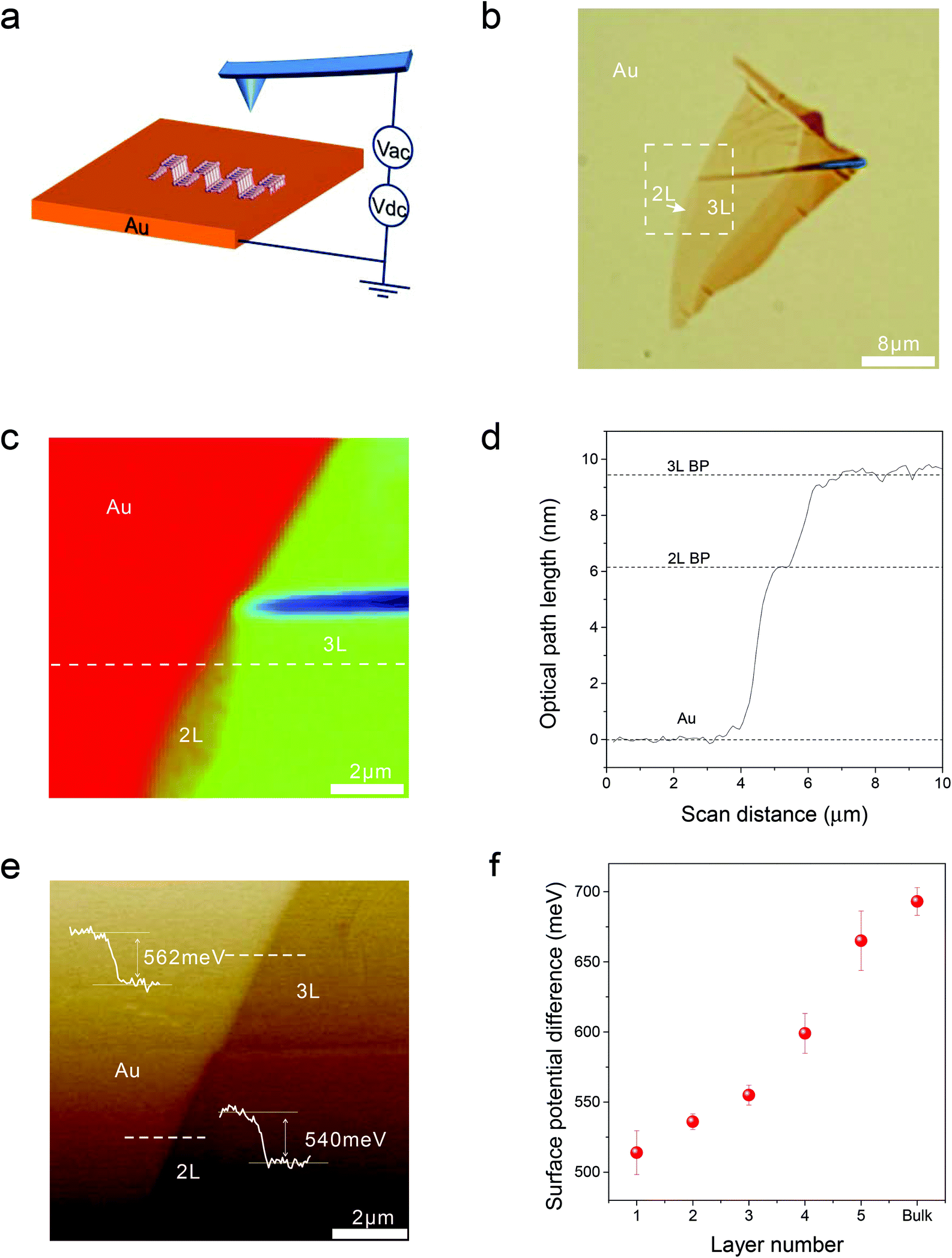 | ||
| Fig. 1 Measured surface potential of mono- and few-layered phosphorene by using a Kelvin probe force microscope (KPFM). (a) Schematic plot of KPFM measurement. (b) Optical microscopy image of the sample with two- and three-layered (2L and 3L) phosphorene on gold substrate. (c) Phase-shifting interferometry (PSI) image of the 2L and 3L phosphorene from the box enclosed by the dashed line in (b). (d) PSI measured optical path length (OPL) values versus scan positions for 2L and 3L phosphorene (or black phosphorous, abbreviated as BP) along the dashed line in (c). The measured optical path length (OPL) values of the sample on gold are 6.2 and 9.4 nm, indicating bi- and tri-layers, respectively (Fig. S1†). (e) Surface potential contour image of the dashed line box region in (b), measured by KPFM. The surface potential differences between the gold substrate and the phosphorene layers (2L and 3L) are also shown, respectively. The surface potential difference between the gold substrate and the phosphorene flake is defined as ϕAu–ϕBP, where ϕAu and ϕBP are the work functions of gold and phosphorene flake, respectively. (f) Measured layer-dependent surface potential differences between the gold substrate and phosphorene flakes. The error bar represents the statistical measurement variations from at least two samples for each layer number. | ||
The layer-dependent surface potential of the phosphorene can enable the engineering of the exciton dynamics in the phosphorene–metal heterostructures, including generation, dissociation, transfer, and recombination, which bears tremendous significance for fundamental and applied interests.18,23 Here, we study charge transfer dynamics in a phosphorene–gold hybrid system using PL spectroscopy (Fig. 2), which has been used to probe the charge transfer in TMD 2D semiconductor heterostructures.16–18,24 In our experiment, few-layered phosphorene flakes were mechanically exfoliated and transferred24 onto the edge of a gold pad, which was prepatterned onto a SiO2/Si (275 nm thermal oxide substrate) substrate. The transfer process was carefully carried out to make sure that half of the few-layered phosphorene flake lies on the SiO2/Si substrate whilst the other half is on the gold (Fig. 2a and b), which will give us precise comparison of the PL emissions from these two halves. From the optical microscopy image (Fig. 2b), the first half of the few-layered phosphorene sample on the SiO2/Si substrate presents much larger contrast than the other half on the gold, which is because the thickness of the SiO2 was pre-designed for the best contrast.25 The layer number was precisely determined by phase-shift interferometry (PSI) (Fig. 2c & d, Fig. S2 & S3†), which has been demonstrated to be a fast and precise way to identify the layer number of phosphorene in our previous report.26 The layer number identification was also confirmed by comparing the measured PL spectra with our previous reports.8,26Fig. 2e shows the measured PL spectra of the bilayered phosphorene samples on both gold and SiO2/Si substrates, using a 532 nm Nd:YAG laser as the excitation source. The PL intensity of the main peak at 945 nm from the 2L phosphorene on Au is much lower than that from the second half of 2L phosphorene on the SiO2/Si substrate, which means that the Au substrate leads to significant PL quenching. This PL quenching is due to the fast interfacial charge transfer between the gold and the 2L phosphorene sample. From the energy diagram shown in Fig. 2f, the photo-excited holes are attracted towards the Au–phosphorene interface and then annihilated by the electrons from the gold.27 Hence, as a consequence of the fast charge transfer, the radioactive recombination will be eliminated, leading to PL quenching in the phosphorene–gold hybrid system.
 | ||
| Fig. 2 Photoluminescence (PL) quenching in the phosphorene–gold hybrid system. (a) Schematic plot of the device structure. A few-layered phosphorene flake was mechanically exfoliated and transferred onto the edge of a gold pad, which was pre-patterned onto a SiO2/Si (275 nm thermal oxide substrate) substrate. The transfer process was carefully carried out to make sure that half of the few-layered phosphorene flake lays on the SiO2/Si substrate whilst the other half is on the gold, which will give us precise comparison of the PL emissions from these two regions. (b) Optical microscopy image of the mechanically transferred few-layered phosphorene flakes, with half on gold and half on SiO2. (c) PSI image of phosphorene samples from the lower box on the SiO2/Si substrate enclosed by the dashed line in (b). (d) PSI measured OPL values versus scan positions for the phosphorene along the dashed line in (c). (e) Measured PL spectra from the 2L phosphorene on Au and SiO2/Si substrates, with the background PL spectra for comparison. (f) Schematic plot of the band diagram, showing the mechanism of PL quenching in the phosphorene–gold hybrid system. | ||
In order to fabricate high-efficiency solar cells based on phosphorene, it is very important to optimize the charge transfer efficiency and thus the carrier collection efficiency in the phosphorene–metal hybrid system.18,28 Owing to the unique puckered structure, phosphorene has been demonstrated to show highly anisotropic properties, such as highly anisotropic excitons,9,29 carrier mobility,30 carrier effective masses,17,30 thermal expansion coefficient31 and shear factor,31 which are all in drastic contrast with the properties of graphene11 and TMD semiconductors.12–14 Therefore, an anisotropic charge transfer in the phosphorene–gold hybrid system could be expected, which makes it more critical to precisely determine the right orientation for the optimized charge transfer. Here, we used the angle-resolved PL quenching measurements to characterize the anisotropic charge transfer in the phosphorene–gold hybrid system. In the setup of the angle-resolved PL measurement, a linearly polarized Nd:YAG laser with a wavelength of 532 nm was used as the excitation source. The polarization angle of the incident light is controlled by an angle-variable half-wave plate. The polarization angle of the PL emission (θ) is characterized by inserting an angle-variable polarizer in front of the detector. We firstly used the excitation polarization dependent PL measurements to determine the crystalline orientation of the 2L phosphorene flake on the SiO2/Si substrate.10 Then the armchair direction is selected as the zero-degree reference for θ (Fig. 3a, inset). Next, we measured the polarization dependence of the PL emission by fixing the excitation polarization along the armchair direction. Fig. 3a presents the polarization dependent PL emission from the first half of the 2L phosphorene flake on the SiO2/Si substrate (Fig. 2b). The red fitting curve shows that the PL intensity follows sinusoid with a period of ∼180°. The PL intensity reaches its maximum at θ = 0° (armchair direction) and its minimum at θ = 90° (zigzag direction), which is consistent with our previous report.10 The measured PL emission from the second half of the 2L phosphorene flake on Au (Fig. 3b) is also linearly polarized, whereas its maximum PL intensity appears at θ = 50° instead of 0°. We attribute this angle difference to be caused by the anisotropic interfacial charge transfer between the phosphorene and gold. Here we use a quenching factor, which is defined by  , to characterize the charge transfer. Fig. 3c shows the measured quenching factor as a function of emission polarization angle. The quenching factor is strongly dependent on the polarization angle, which can be fitted by a sinusoidal curve with a period of ∼180°. The measured maximum quenching factor was 6, which occurs at θ = 0°, while the minimum quenching factor is 1.5, which occurs at θ = 90°. This strongly anisotropic PL quenching can be understood by the anisotropic interfacial charge transfer between the phosphorene and gold. Since the PL quenching effect between the semiconductor materials and metals is basically due to the transport of photo-excited charges,24,27 phosphorene has the maximum charge mobility along the armchair direction,32 which leads to the maximum speed of charge transfer and thus the maximum quenching factor along the armchair direction.
 | ||
Fig. 3 Anisotropic PL quenching/charge transfer in the phosphorene–gold hybrid system. (a and b) Measured PL peak intensities as a function of the emission polarization angle θ, from the 2L phosphorene sample, half on SiO2/Si (a) and the second half on gold (b), respectively. The red lines are the fitted sinusoidal curves. Inset: schematic plot of the top view of the phosphorene lattice structure and coordinates for the polarization angle θ. (c) The measured PL quenching factor from the 2L phosphorene sample, as a function of emission polarization angle. The quenching factor is defined by  . The red line is the fitted sinusoidal curve. . The red line is the fitted sinusoidal curve. | ||
Besides the charge mobility discussed above, the Schottky energy barrier is another important factor to determine the efficiency of interfacial charge transfer.17,18 Previous calculations have predicted that phosphorene has a layer-dependent band alignment and there is a significant shift of the valence band edge upon thickness variation, which can be useful for tuning the Schottky barrier to promote the hole injection efficiency.33 This prediction is confirmed from our following layer-dependent PL quenching experiments in the phosphorene–gold hybrid system. The measured quenching factor of a 3L phosphorene on Au is around one order of magnitude higher than that of a 2L phosphorene, for emission polarization of both zigzag and armchair directions (Fig. 4a), respectively. This strong layer-dependent PL quenching in phosphorene is in great contrast with that in MoS2, where the quenching factor does not cause large changes for mono- and few-layered MoS2.24 The layer-dependent PL quenching in the phosphorene–gold hybrid system can be understood from their band diagrams, as shown in Fig. 4b. The band diagrams were generated based on the calculated valence band maximum (VBM) and conduction band minimum (CBM) for few-layered phosphorene19 and our measured surface potential difference between phosphorene and Au. As shown in Fig. 1f, the measured surface potential difference between 3L phosphorene and gold (∼555 meV) is larger than that for 2L phosphorene (∼536 meV), which results in a larger Schottky barrier for the 3L phosphorene–Au hybrid system than that for 2L phosphorene (Fig. 4b). This larger Schottky barrier will increase the force to pull holes towards the phosphorene–gold interface, leading to more efficient interfacial charge transfer and thus much larger PL quenching for 3L than 2L phosphorene in the phosphorene–gold hybrid system.
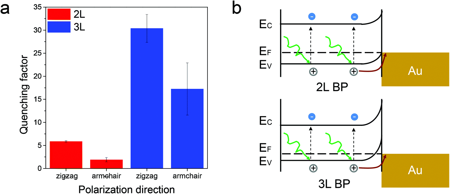 | ||
| Fig. 4 Layer-dependent PL quenching/charge transfer in the phosphorene–gold hybrid system. (a) Measured PL quenching factors from 2L and 3L phosphorene samples, with emission polarization angles along the armchair and zigzag directions, respectively. The error bar represents the statistical measurement variation from at least two samples. (b) Schematic plot of the band diagrams for 2L and 3L phosphorene–gold hybrid systems. The band diagrams were generated based on the calculated valence band maximum (VBM) and conduction band minimum (CBM) for few-layered phosphorene19 and our measured surface potential difference between phosphorene and Au. | ||
Conclusions
In conclusion, we directly measured the layer-dependent surface potential of mono- and few-layered phosphorene on a gold substrate, which is consistent with the reported theoretical prediction.19 At the same time, we used an optical way PL spectroscopy to probe charge transfer in a phosphorene–gold hybrid system. We firstly observed highly anisotropic and layer-dependent PL quenching, which is attributed to the highly anisotropic/layer-dependent interfacial charge transfer in the phosphorene–gold hybrid system. Our results open the door for designing future electronic and optoelectronic heterostructure devices using phosphorene.Experimental methods
We used mechanical exfoliation to transfer34 a phosphorene flake onto the edge of a pre-patterned gold electrode on a SiO2/Si substrate (275 nm thermal oxide on n+-doped silicon). The gold electrodes were patterned by conventional photolithography, metal deposition, and lift-off processes. All PL and polarization measurements were conducted using a T64000 micro-Raman system equipped with a charge-coupled device (CCD) and InGaAs detectors, along with a 532 nm Nd:YAG laser as the excitation source. Subsequent to PSI measurement, the sample was placed into a Linkam THMS 600 chamber, with a slow flow of nitrogen gas to prevent degradation of the sample.8 To avoid laser-induced sample damage, all PL spectra were recorded at low power levels: P ∼ 20 μW. The surface potential was measured by KPFM. The model of the KPFM used in the experiments was Bruker Multimode VIII with Peak Force TUNA.Competing financial interests
The authors declare that they have no competing financial interests.Acknowledgements
We would like to thank Professor Chennupati Jagadish and Professor Barry Luther-Davies from The Australian National University, for their facility support. We acknowledge financial support from ANU PhD student scholarship, the China Scholarship Council, Australian Research Council (grant no. DE140100805), and ANU Major Equipment Committee (grant no. 14MEC34).References
- H. Liu, A. T. Neal, Z. Zhu, Z. Luo, X. Xu, D. Tománek and P. D. Ye, ACS Nano, 2014, 8, 4033–4041 CrossRef CAS PubMed.
- M. Buscema, D. J. Groenendijk, S. I. Blanter, G. A. Steele, H. S. J. van der Zant and A. Castellanos-Gomez, Nano Lett., 2014, 14, 3347–3352 CrossRef CAS PubMed.
- R. Fei and L. Yang, Nano Lett., 2014, 14, 2884–2889 CrossRef CAS PubMed.
- F. Xia, H. Wang and Y. Jia, Nat. Commun., 2014, 5 Search PubMed.
- L. Li, Y. Yu, G. J. Ye, Q. Ge, X. Ou, H. Wu, D. Feng, X. H. Chen and Y. Zhang, Nat. Nanotechnol., 2014, 9, 372–377 CrossRef CAS PubMed.
- T. Hong, B. Chamlagain, W. Lin, H.-J. Chuang, M. Pan, Z. Zhou and Y.-Q. Xu, Nanoscale, 2014, 6, 8978–8983 RSC.
- J. Qiao, X. Kong, Z.-X. Hu, F. Yang and W. Ji, Nat. Commun., 2014, 5 CAS.
- S. Zhang, J. Yang, R. Xu, F. Wang, W. Li, M. Ghufran, Y.-W. Zhang, Z. Yu, G. Zhang, Q. Qin and Y. Lu, ACS Nano, 2014, 8, 9590–9596 CrossRef CAS PubMed.
- V. Tran, R. Soklaski, Y. Liang and L. Yang, Phys. Rev. B: Condens. Matter, 2014, 89, 235319 CrossRef.
- S. Zhang, R. Xu, F. Wang, J. Yang, Z. Wang, J. Pei, Y. W. Myint, B. Xing, Z. Yu, L. Fu, Q. Qin and Y. Lu, 2014, arXiv:1411.6124.
- A. K. Geim and K. S. Novoselov, Nat. Mater., 2007, 6, 183–191 CrossRef CAS PubMed.
- B. Radisavljevic, A. Radenovic, J. Brivio, V. Giacometti and A. Kis, Nat. Nanotechnol., 2011, 6, 147–150 CrossRef CAS PubMed.
- K. F. Mak, K. He, C. Lee, G. H. Lee, J. Hone, T. F. Heinz and J. Shan, Nat. Mater., 2013, 12, 207–211 CrossRef CAS PubMed.
- J. S. Ross, S. Wu, H. Yu, N. J. Ghimire, A. M. Jones, G. Aivazian, J. Yan, D. G. Mandrus, D. Xiao, W. Yao and X. Xu, Nat. Commun., 2013, 4, 1474 CrossRef PubMed.
- J. Yang, T. Lü, Y. W. Myint, J. Pei, D. Macdonald, J.-C. Zheng and Y. Lu, ACS Nano, 2015, 9, 6603–6609 CrossRef CAS PubMed.
- J. Yuan, S. Najmaei, Z. Zhang, J. Zhang, S. Lei, P. M. Ajayan, B. I. Yakobson and J. Lou, ACS Nano, 2015, 9, 555–563 CrossRef CAS PubMed.
- X. Hong, J. Kim, S.-F. Shi, Y. Zhang, C. Jin, Y. Sun, S. Tongay, J. Wu, Y. Zhang and F. Wang, Nat. Nanotechnol., 2014, 9, 682–686 CrossRef CAS PubMed.
- Y. Yu, S. Hu, L. Su, L. Huang, Y. Liu, Z. Jin, A. A. Purezky, D. B. Geohegan, K. W. Kim, Y. Zhang and L. Cao, Nano Lett., 2015, 15, 486–491 CrossRef CAS PubMed.
- Y. Cai, G. Zhang and Y.-W. Zhang, Sci. Rep., 2014, 4 Search PubMed.
- J. Yang, R. Xu, J. Pei, Y. W. Myint, F. Wang, Z. Wang, S. Zhang, Z. Yu and Y. Lu, Light Sci. Appl., 2015, 4, e312 CrossRef CAS.
- M. Nonnenmacher, M. P. O'Boyle and H. K. Wickramasinghe, Appl. Phys. Lett., 1991, 58, 2921–2923 CrossRef.
- Y. Li, C.-Y. Xu and L. Zhen, Appl. Phys. Lett., 2013, 102, 143110 CrossRef.
- S. Das, W. Zhang, M. Demarteau, A. Hoffmann, M. Dubey and A. Roelofs, Nano Lett., 2014, 14, 5733–5739 CrossRef CAS PubMed.
- U. Bhanu, M. R. Islam, L. Tetard and S. I. Khondaker, Sci. Rep., 2014, 4 Search PubMed.
- M. Benameur, B. Radisavljevic, J. Heron, S. Sahoo, H. Berger and A. Kis, Nanotechnology, 2011, 22, 125706 CrossRef CAS PubMed.
- J. Yang, R. Xu, J. Pei, Y. W. Myint, F. Wang, Z. Wang, S. Zhang, Z. Yu and Y. Lu, 2015, arXiv:1504.06386v2.
- Z. Yin, H. Li, H. Li, L. Jiang, Y. Shi, Y. Sun, G. Lu, Q. Zhang, X. Chen and H. Zhang, ACS Nano, 2012, 6, 74–80 CrossRef CAS PubMed.
- M.-L. Tsai, S.-H. Su, J.-K. Chang, D.-S. Tsai, C.-H. Chen, C.-I. Wu, L.-J. Li, L.-J. Chen and J.-H. He, ACS Nano, 2014, 8, 8317–8322 CrossRef CAS PubMed.
- X. Wang, A. M. Jones, K. L. Seyler, V. Tran, Y. Jia, H. Zhao, H. Wang, L. Yang, X. Xu and F. Xia, 2014, arXiv preprint arXiv:1411.1695.
- J. Qiao, X. Kong, Z.-X. Hu, F. Yang and W. Ji, Nat.commun., 2014, 5 CAS.
- S. Appalakondaiah, G. Vaitheeswaran, S. Lebegue, N. E. Christensen and A. Svane, Phys. Rev. B: Condens. Matter, 2012, 86, 035105 CrossRef.
- Y. Deng, Z. Luo, N. J. Conrad, H. Liu, Y. Gong, S. Najmaei, P. M. Ajayan, J. Lou, X. Xu and P. D. Ye, ACS Nano, 2014, 8, 8292–8299 CrossRef CAS PubMed.
- K. H. Li, X. Liu, Q. Wang, S. Zhao and Z. Mi, Nat. Nanotechnol., 2015, 10, 140–144 CrossRef CAS PubMed.
- A. Castellanos-Gomez, M. Buscema, R. Molenaar, V. Singh, L. Janssen, H. S. J. v. d. Zant and G. A. Steele, 2D Mater., 2014, 1, 011002 CrossRef.
Footnote |
| † Electronic supplementary information (ESI) available: Details of theoretical calculation methods, more experimental measurement results and data analysis. See DOI: 10.1039/c5nr04366b |
| This journal is © The Royal Society of Chemistry 2016 |