
Electrophoretic deposition of fluorescent Cu and Au sheets for light-emitting diodes†
Jiale
Liu
a,
Zhennan
Wu
a,
Tingting
Li
a,
Ding
Zhou
a,
Kai
Zhang
a,
Yu
Sheng
*b,
Jianli
Cui
*c,
Hao
Zhang
*a and
Bai
Yang
a
aState Key Laboratory of Supramolecular Structure and Materials, College of Chemistry, Jilin University, Changchun 130012, P. R. China. E-mail: hao_zhang@jlu.edu.cn
bDepartment of Dermatology, First Affiliated Hospital, Harbin Medical University, Harbin 150001, P. R. China. E-mail: sf555812@163.com
cDepartment of Hand & Foot Surgery, The First Hospital of Jilin University, Changchun 130021, P. R. China. E-mail: tsuijianli@126.com
First published on 30th November 2015
Abstract
Electrophoretic deposition (EPD) is a conventional method for fabricating film materials from nanometer-sized building blocks, and exhibits the advantages of low-cost, high-efficiency, wide-range thickness adjustment, and uniform deposition. Inspired by the interest in the application of two-dimensional (2D) nanomaterials, the EPD technique has been recently extended to building blocks with 2D features. However, the studies are mainly focused on simplex building blocks. The utilization of multiplex building blocks is rarely reported. In this work, we demonstrate a controlled EPD of Cu and Au sheets, which are 2D assemblies of luminescent Cu and Au nanoclusters. Systematic investigations reveal that both the deposition efficiency and the thickness are determined by the lateral size of the sheets. For Cu sheets with a large lateral size, a high ζ-potential and strong face-to-face van der Waals interactions facilitate the deposition with high efficiency. However, for Au sheets, the small lateral size and ζ-potential limit the formation of a thick film. To solve this problem, the deposition dynamics are controlled by increasing the concentration of the Au sheets and adding acetone. This understanding permits the fabrication of a binary EPD film by the stepwise deposition of Cu and Au sheets, thus producing a luminescent film with both Cu green emission and Au red emission. A white light-emitting diode prototype with color coordinates (x, y) = (0.31, 0.36) is fabricated by employing the EPD film as a color conversion layer on a 365 nm GaN clip and further tuning the amount of deposited Cu and Au sheets.
1. Introduction
For the last few years, two-dimensional (2D) nanomaterials have drawn a lot of attention owing to their unique structures and charming properties.1–3 These greatly inspire the attempts to use 2D nanomaterials in photoelectric and photovoltaic devices,4 supercapacitors,5,6 lithium batteries,7 transistors,8,9 catalysis,10 and so forth. 2D nanomaterials can be composed of various organic and inorganic compositions. Organic 2D materials mainly relate to carbon-containing materials, such as graphene and 2D polymers.11–13 Inorganic 2D materials include hexagonal boron nitride (h-BN),14 transition metal dichalcogenides (MoS2, WS2),15,16 metal halides (PbI2, MgBr2),17 metal oxides (MnO2, MoO3, LaNb2O7),18,19 and layered semiconductors (CdS, CdSe, InSe, Bi2Te3).8,20–28 They appear as mono-, few-, or multi-layered sheets. Recently, a new type of 2D materials, which are fabricated through the self-assembly of preformed nanoclusters (NCs) or nanowires, have started to gain attention, because they simultaneously possess the properties of 2D materials and of the original building blocks.29–40 For example, 2D thin films of metal NCs have been applied as quantum emitters for light-emitting diodes (LEDs).41With respect to photoelectric and photovoltaic applications, the spatial distribution of 2D building blocks in films is the key to determine the performance. 2D anisotropy is generated only when the building blocks are uniformly arranged parallel along or perpendicular to the substrates.42,43 However, in conventional film preparation, 2D building blocks are deposited on substrates uncontrollably, which leads to a random distribution in the films. Better methods for directing the oriented arrangement of 2D building blocks are greatly welcomed.44
Electrophoretic deposition (EPD) is a low-cost and high-efficiency processing technique for fabricating films on any shaped substrate with high deposition efficiency, wide-range thickness adjustment, and uniformity of deposits.45,46 Over the last few years, these advantages have made EPD a promising technique for producing film materials from nanometer-sized building blocks with a variety of compositions.47–57 The EPD process includes two steps. First, charged nanoparticles in a colloidal suspension are forced by an electric field and move to the electrode with the opposite charge. Second, these nanoparticles are deposited on the electrode surface and form a compact film. EPD possesses size- and shape-selectivity, and has the capability to separate nanoparticles with different sizes and shapes.58,59 Inorganic nanoplatelets and graphene sheets with a larger lateral size are easier to deposit on electrodes than spherical particles.60 In this context, the larger lateral size provides bigger ζ-potentials and face-to-face van der Waals (vdW) interactions.60 As a result, 2D materials have higher electrophoretic mobility under an electric field than 1D and 0D ones.58–60 Despite the success in the EPD of 2D nanomaterials, the efforts are mainly focused on simplex materials.61,62 Deposition with multiplex materials is rarely reported. In many applications, the co-deposition of different 2D materials in a controlled manner is strongly required.63–65
In this paper, co-deposition films, composed of Cu and Au NC self-assembly sheets, are fabricated following a stepwise EPD strategy. Fluorescent Cu and Au sheets are prepared by assembling green-emitting Cu and red-emitting Au NCs in organic media. In chloroform, a controlled EPD is operated by altering the species and concentrations of the 2D sheets, deposition duration, voltage, and additional solvent, which produces fluorescent films with both Cu green emission and Au red emission. The films are further employed as a color conversion layer on a 365 nm GaN clip to fabricate white LEDs (WLEDs). A WLED prototype with color coordinates (x, y) = (0.31, 0.36), color temperature of 6577 K, and color rendering index (CRI) of 88 is fabricated by tuning the amount of deposited Cu and Au sheets.
2. Experimental
2.1. Materials
HAuCl4·4H2O was purchased from Sinopharm Chemical Reagent Co., Ltd. CuCl2·2H2O was purchased from Alfa Aesar. 1-Dodecanethiol (DT, 98%) was purchased from Aladdin. Dibenzyl ether (BE) was purchased from Aldrich. Liquid paraffin (LP), acetone, and chloroform were used as received without further purification. Ultraviolet GaN LEDs with an emission peak at 365 nm were purchased from Advanced Optoelectronic Technology Inc. The unpacked LEDs have a 1.42 mm × 1.42 mm chip.2.2. Preparation of Cu NC self-assembly sheets
Cu sheets were synthesized by stirring a mixture of 60 mg of CuCl2·2H2O, 12 mL of LP, and 2 mL of DT at 50 °C for 10 h. A 1 mL white suspension of the product was washed and precipitated by adding 1 mL of chloroform and 2 mL of acetone. After that, the products were separated by centrifugation at 7500 rpm for 5 min. The purification process was repeated twice. Finally, the Cu sheets were dispersed in 1 mL of chloroform.2.3. Preparation of Au NC self-assembly sheets
0.2 g of HAuCl4·4H2O was first dissolved in 2 mL of BE in a 100 mL three-neck flask. Then, 15 mL of LP and 0.5 mL of DT were added into the flask. The mixture was slowly heated under vacuum for 10 min, and then quickly heated to 142 °C under nitrogen protection. The mixture was maintained at 142 °C for 1 h. Finally, the mixture was slowly cooled to room temperature. The purification process was the same as that for the Cu sheets.2.4. Electrophoretic deposition
The EPD was operated using a high-voltage DC power supply. Indium tin oxide (ITO) covered glasses with a resistance of 10 ohm sq−1 was used as an electrode. The size of the ITO glass was 4 cm × 2 cm. The distance between the cathode and anode was 6.5 mm. Half of the electrodes were immersed into the chloroform suspensions of Cu and Au sheets with specific concentrations. The voltage was varied between 100 and 500 V. To calculate the mass of deposited sheets, the cathode was weighed before and after deposition.2.5. Fabrication of LEDs
To fabricate LEDs from EPD films, the ITO glasses, which were deposited with Cu and/or Au sheets, were incised into 6 mm × 6 mm pieces and put on the top of a 365 nm GaN LED chip.2.6. Characterization
UV-visible absorption spectra were obtained using a Shimadzu 3600 UV-VIS-NIR spectrophotometer. Photoluminescence (PL) spectroscopy was performed using a Shimadzu RF-5301 PC spectrophotometer with an excitation of 365 nm. The absolute quantum yields (QYs) were measured using a Edinburgh FLS920 (excited at 365 nm) equipped with an integrating sphere. Transmission electron microscopy (TEM) was conducted using a Hitachi H-800 electron microscope at an acceleration voltage of 200 kV with a CCD camera. Atomic force microscopy (AFM) tapping mode measurements were performed with a Nanoscope IIIa scanning probe microscope (Digital Instruments) using a rotated tapping mode etched silicon probe tip. X-ray diffraction (XRD) investigations were carried out on a Rigaku X-ray diffractometer using Cu Kα radiation (λ = 1.5418 Å). Scanning electron microscopy (SEM) images were recorded with a JEOL FESEM 6700F electron microscope using a primary electron energy of 3 kV and the samples were sputtered with Pt before testing and mapping images were recorded at 15 kV without sputtering with Pt. ζ-Potentials were measured using a Zetasizer NanoZS (Malvern Instruments). The emission colors and spectra of the LED devices were identified using the CIE (Commission Internationale de L'Echairage 1931) colorimetry system.3. Results and discussion
3.1. Cu and Au NC self-assembly sheets
The Cu and Au sheets used for EPD were prepared through the self-assembly of Cu(0)4Cu(I)10DT10 and Au(0)11Au(I)4DT15 NCs in organic media according to our previous methods.29,30 The resultant Cu sheets exhibit an average thickness of 159 nm and a lateral size of several micrometers (Fig. 2a and b). Different from the original non-fluorescent Cu NCs, the Cu sheets exhibit blue-green emission when excited by 365 nm UV-light (Fig. S1a†). The emission peak centers at 491 nm with a full width at half maximum (FWHM) of 77 nm (Fig. 2c). The Au sheets have a regular hexagonal morphology and are 2.5 μm in length, 1.2 μm in width, and 162 nm in thickness (Fig. 2d and e). The emission peak of the Au sheets centers at 601 nm with a FWHM of 65 nm when excited by 365 nm UV-light, which is the same as the original Au NCs (Fig. 2f and S1b†). Powders of the Cu and Au sheets indicate PLQYs of 4.6% and 1.1%, respectively. Both Cu and Au sheets can be well dispersed in common organic solvents, such as chloroform.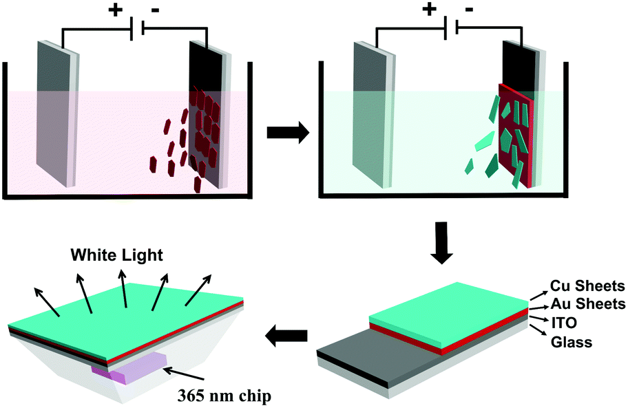 | ||
| Fig. 1 Schematic illustration of the stepwise deposition of Au and Cu fluorescent sheets on ITO and further coating them on a 365 nm GaN chip for fabricating a WLED. | ||
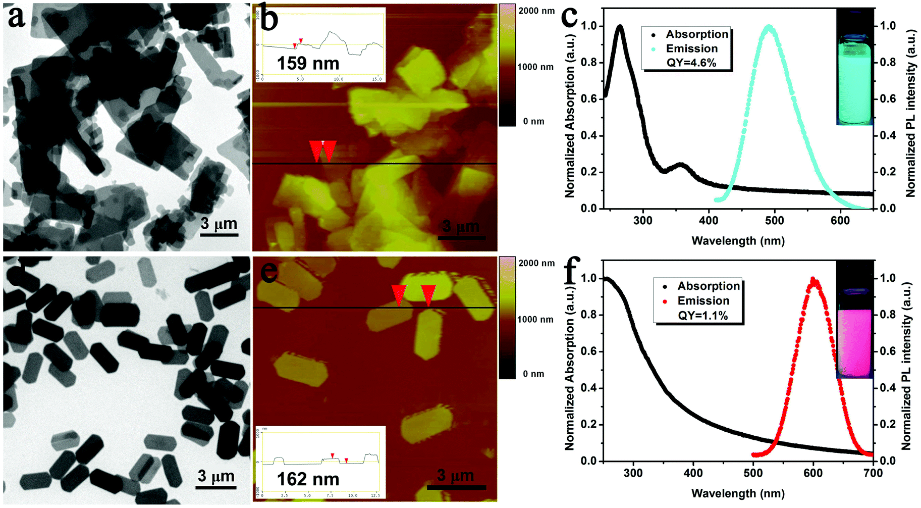 | ||
| Fig. 2 TEM (a) and tapping-mode AFM (b) images, and UV-vis absorption and PL spectra (c) of Cu sheets. TEM (d) and tapping-mode AFM (e) images, and UV-vis absorption and PL spectra (f) of Au sheets. Insets in (c) and (f): PL images of Cu and Au sheet chloroform suspensions when excited by 365 nm UV-light. | ||
3.2. EPD of Cu sheets
To produce EPD films from Cu sheets, 8 mg of the Cu sheets were dispersed in 10 mL of chloroform and deposited on ITO glass under 200 V for 5 min with an electrode distance of 6.5 mm (equivalent to an electric field of 308 V cm−1). A smooth film was observed on the electrode. When excited by 365 nm UV-light, the film exhibits a strong blue-green emission, which is the same as for the Cu sheets (Fig. 3c and d). From the top view SEM image of the film (Fig. 3a), the deposited Cu sheets are found to be parallel on the electrode. This is attributed to the large lateral size of the Cu sheets, which leads to strong face-to-face vdW interactions.59,60 Consequently, they prefer to deposit in a face-to-face manner. The cross sectional SEM image reveals that the thickness of the face-to-face stacked Cu sheet film is around 20 μm (Fig. 3b), which is the thickness of more than one hundred Cu sheets. The aforementioned results clearly indicate that a smooth Cu sheet film can be easily fabricated on ITO through EPD. To further control the EPD process, the deposition dynamics were studied on the basis of the Hamaker equation:66 | (1) |
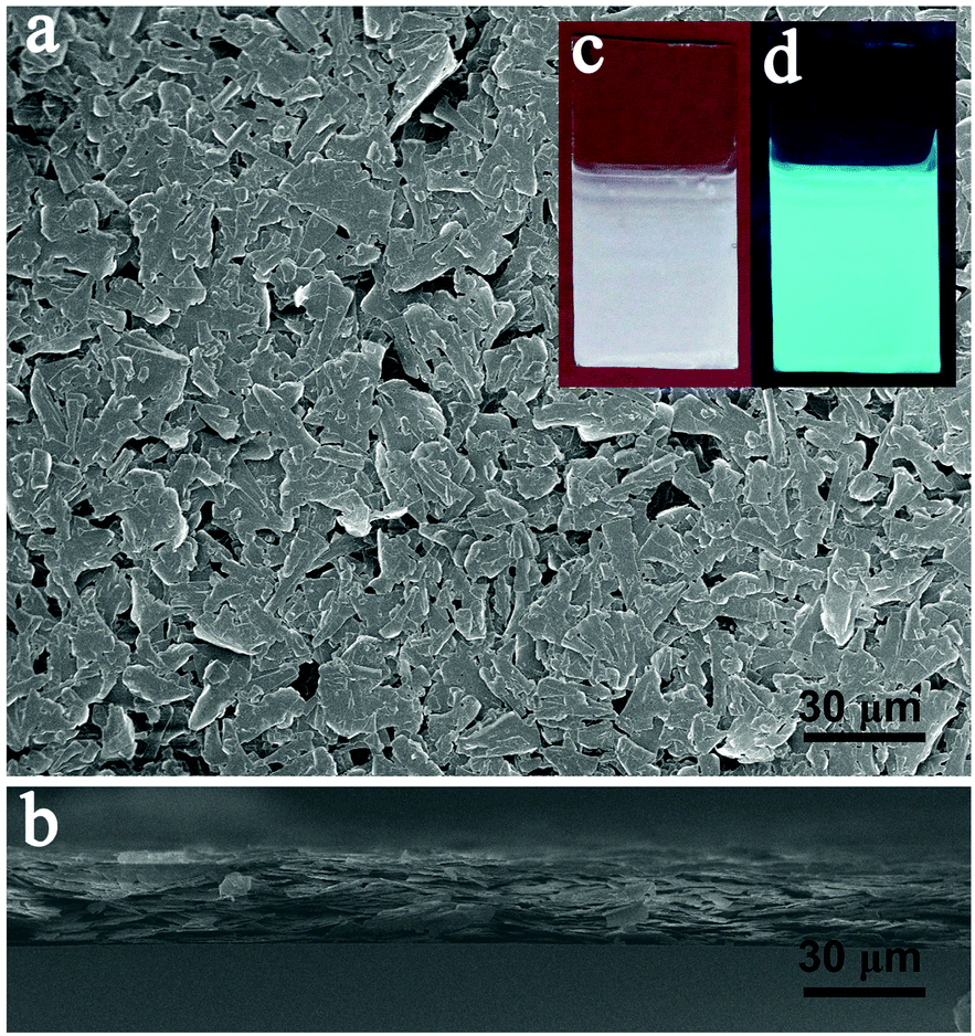 | ||
| Fig. 3 Top view (a) and cross sectional (b) SEM images of the Cu sheet film deposited under 200 V for 5 min. Optical (c) and PL (d) images of the Cu sheet film excited by 365 nm ultraviolet light. | ||
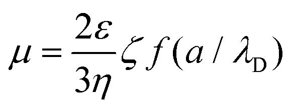
At the same time, the electrophoretic mobility μ can be estimated by the following equation:59
 | (2) |
Here, μ is the electrophoretic mobility, ζ is the ζ-potential, ε and η are the solvent dielectric constant and viscosity, f is Henry's function which depends on a, the nanoparticle diameter, and λD, the Debye length.
No matter how a/λD is altered, f only ranges between 1 and 1.5. So, μ is nearly proportional to ζ as the solvent is fixed. The value only relates to the material itself and the species of solvent rather than voltage, concentration, or other experimental variables. According to eqn (1), the deposition speed dY/dt is proportional to k, μ, Cs, E, and A. k and μ only relate to the materials and solvents. The alteration of A only affects the deposited mass rather than the thickness of the film. So, once the materials, solvents, and A are fixed, the deposited mass Y can be controlled by adjusting Cs, E, and t. In another words, the thickness of the film is potentially controllable by varying Cs, E, and t with a fixed A.
To confirm the concentration range for EPD, the influence of the concentration of Cu sheets on the deposition speed was investigated first. The key was to control the film thickness over a large range. By fixing A, the mass of the Cu sheet film is weighed after EPD with different deposition durations and concentrations of Cu sheets. Fixing the concentration of the Cu sheets at 0.2 mg mL−1, the film forms slowly (Table S1†). When the concentration of the Cu sheets reaches 0.8 mg mL−1, the mass increment is more than 4 times that of the 0.2 mg mL−1 suspension. The concentration-dependent deposition speed is clearly indicated in Fig. 4. According to the Hamaker equation, the deposition speed should be in direct proportion to k, μ, Cs, E, and A under ideal conditions. However, in our investigation, Cs, the suspension concentration, continuously decreases during the deposition process, because the initial Cs is high. Consequently, the deposition speed gradually decreases during the deposition. When the initial Cs is low enough, the deposition speed is nearly fixed, which is in accordance with the Hamaker equation (Fig. 4). Note that, at any concentration, the deposition speed decreases after the initial several minutes of deposition, which results from a decrease in the concentration of the Cu sheets. It is hard for all of the Cu sheets to be deposited on ITO glass, in particular at low concentration. Relatively high concentration is favorable for controlling the thickness of the Cu sheets over a large range. Therefore, an 0.8 mg mL−1 concentration of the Cu sheets was selected for further EPD.
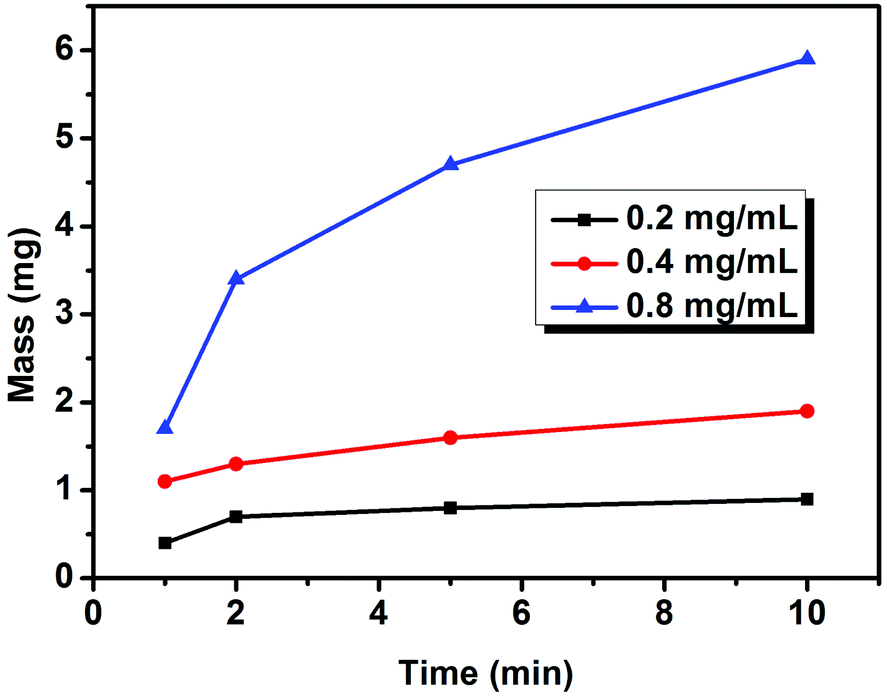 | ||
| Fig. 4 The increase of film mass versus deposition duration at different concentrations of Cu sheets. The voltage is 200 V. | ||
Furthermore, the influence of EPD voltage is revealed by altering the working voltage from 100 to 500 V (Fig. 5). The mass variation of the films is shown in Table S2.† The corresponding optical and fluorescence images are provided in Fig. S2.† In general, an increase in the voltage accelerates the EPD. When the voltage is 100 V, the film mass increases slowly over the tested 30 min. But when the voltage is raised to 500 V, the mass increment becomes very fast at the beginning. The deposition speed starts to slow down after 15 min because of the concentration decrease by continuously depositing Cu sheets on ITO. The voltage is in direct proportion to the electric field intensity under a fixed electrode distance. According to eqn (1), the deposition speed directly relates to voltage. Summarizing the film mass data, the deposition mass of the Cu sheets can be tuned by altering the deposition voltage and the duration under a proper concentration.
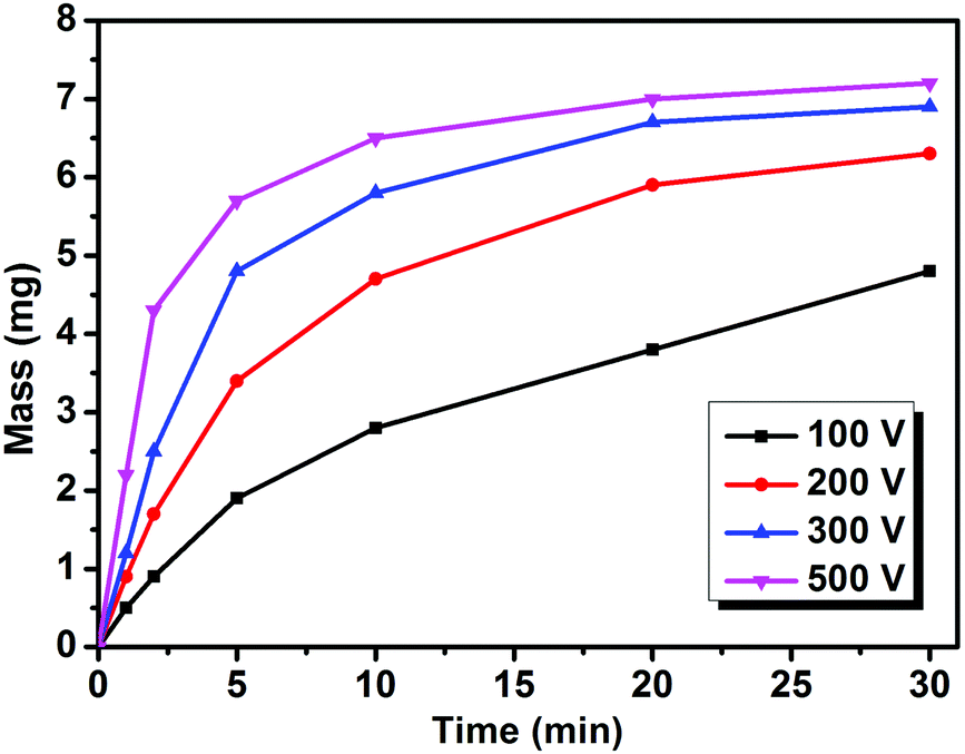 | ||
| Fig. 5 The increase in the film mass versus deposition duration under different voltages. The concentration of the Cu sheets is 0.8 mg mL−1. | ||
In order to convert film mass into film thickness, the relationship between the film mass and thickness is built on the basis of the SEM observations (Fig. S3†). A series of films with different masses were prepared under the conditions of 100 V for 1 min, 300 V for 1 min, 500 V for 1 min, 300 V for 2 min, and 500 V for 2 min. Whereas, the concentration of the Cu sheets, suspension volume, and electrode distance were fixed at 0.8 mg mL−1, 10 mL, and 6.5 mm, respectively. The thickness was measured through the analysis of cross sectional SEM images (Fig. S3b–f†). By summarizing the mass and thickness of the films, a linear relationship was confirmed (Fig. S3a†). The thickness-to-mass ratio is 8.7 μm mg−1 as deposited on the ITO glass with an area of 4.3 cm2. As calculated, the density of the film is about 0.27 g cm−3.
3.3. EPD of Au sheets
The deposition speed of the Au sheets is much slower than that of the Cu sheets. For example, 30 min deposition under the conditions of the concentration of Au sheets at 1 mg mL−1, voltage of 200 V, and electrode distance of 6.5 mm only produces thin films. In comparison with the Cu sheets, the Au sheets have a lower ζ-potential and lateral size. The ζ-potential of the Cu sheets in chloroform is 13 mV, while it is 2.4 mV for the Au sheets. On the one hand, the ζ-potential is proportional to the electrophoretic mobility μ. The low ζ-potential of the Au sheets reduces μ. On the other hand, the small lateral size of the Au sheets decreases the tendency of face-to-face deposition due to the lower face-to-face vdW interactions.59,60 These decrease the contribution to deposition efficiency k. As a result, the deposition yield Y of the Au sheets is lower than that of the Cu sheets. To increase the deposition yield of the Au sheets, the electrophoretic mobility μ and concentration Cs should be further increased. According to eqn (2), μ is proportional to the solvent dielectric constant ε. So, the addition of a secondary solvent with a dielectric constant higher than that of chloroform will increase μ. In this scenario, the ε of acetone is 21.5, while the ε of chloroform is 5.1. The addition of acetone is considered to enhance the deposition yield. In addition, acetone also promotes the aggregation of Au sheets because of the larger polarity. The aggregation of Au sheets increases the size of the building blocks, and therefore the μ. Consequently, the EPD in chloroform and acetone mixtures greatly increases the deposition yield of the Au sheets (Fig. 6a). By further increasing the concentration of the Au sheets, the deposition yield is greatly increased. Through this improvement, most of the Au sheets are deposited face-to-face (Fig. 6b and c).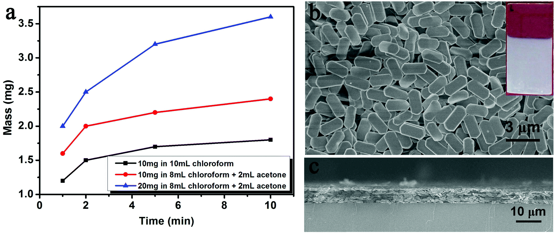 | ||
| Fig. 6 (a) The increase of film mass versus deposition duration in chloroform and acetone mixtures. The voltage is 200 V. Top view (b) and cross sectional (c) SEM images of the Au sheet film deposited under 200 V for 5 min with 20 mg of Au sheets in 8 mL of chloroform and 2 mL of acetone. | ||
3.4. Stepwise deposition of Cu and Au sheets for WLEDs
The aforementioned results indicate that the EPD of Cu or Au sheets alone can be well controlled, which produce films with strong luminescence. This experience is extended to fabricate co-deposition films composed of Cu and Au sheets. With regard to the application in WLEDs, Au sheets should be put close to the GaN LED chip for two reasons. First, the PLQY of the Au sheets is weaker than that of the Cu sheets. The placement of Au near the LED chip can enhance the absorption of UV-light, and hence the emission intensity. Second, the blue-green emission of the Cu sheets can be re-absorbed by the Au sheets, because the energy of the blue-green emission is higher than that of the red emission.67,68 Such re-absorption is common in fabricating LEDs from multiplex emitting components, which makes it difficult to design and fabricate WLEDs.69 In the current EPD, the deposition efficiency of the Au sheets is lower than that of the Cu sheets. So, the sequence of deposition should be Au and then Cu. In the resultant EPD films, Au sheets attach onto the ITO glass, while the Cu sheets are on the surface. The co-deposition of Au and Cu sheets is proved by small angle XRD. Both the characteristic peaks of the Au and Cu sheets are observed, showing the co-existence of them. Because the Cu sheets are on the film surface, they give a stronger signal than the Au sheets (Fig. 7a). From the cross sectional SEM image of the film, the Au and Cu layers are clearly distinguishable. The Cu and Au elements are also exhibited by mapping images (Fig. 7b–d). Fig. 7e and f show the optical and PL images of the co-deposited film. To clearly show Au and Cu emission, the Cu sheets are deposited only on half of the Au film. When excited by 365 nm UV-light, both the Au sheet red emission and Cu sheet green emission are observed. Note that although the films are fabricated using a two step deposition, the deposition dynamics are the same as depositing Cu and Au sheets alone. In particular, when immersing the as-deposited Au sheets in a Cu sheet suspension, the Au sheets do not fall off, because the deposition speed of the Cu sheets is rather high for their large lateral size. Cu sheets rapidly cover the as-deposited Au sheets, thus preventing the loss of Au sheets.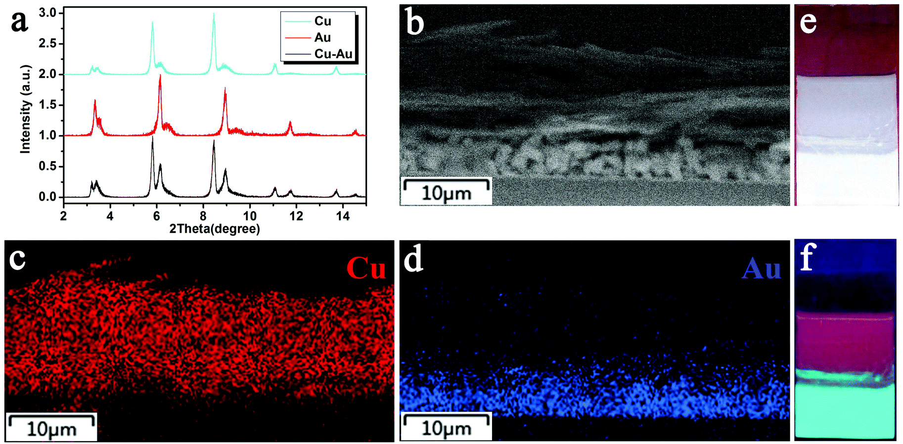 | ||
| Fig. 7 (a) Small angle XRD patterns of Cu, Au and Cu–Au films. (b) Cross sectional SEM image of the Cu–Au co-deposited film. SEM mapping images for Cu (c) and Au (d) elements. Optical (e) and PL (f) images of the Cu–Au co-deposited film excited by 365 nm UV-light. | ||
LED devices were fabricated by covering the EPD films on a commercial GaN clip with 365 nm emission. The EPD films act as a color conversion layer by adsorbing GaN emission and emitting the characteristic emission of Au and/or Cu sheets. The LEDs with blue-green and red emission are fabricated respectively using the EPD films from Cu and Au sheets. They indicate strong blue-green and red emission with the color coordinates (x, y) = (0.55, 0.35), and (0.21, 0.43) (Fig. 8a and c). WLEDs were further fabricated by stepwise deposition of Au and Cu sheets as shown in Fig. 1. In tuning the ratio of the deposited Au and Cu sheets, the Au sheets are deposited first at 200 V for 5 min by dispersing 20 mg of the Au sheets in a mixture of 8 mL of chloroform and 2 mL of acetone. Cu sheets are further deposited on the as-deposited Au sheet film at 200 V for 2 min with 8 mg of Cu sheets dispersed in 10 mL of chloroform. A primary WLED prototype indicates the color coordinates (x, y) = (0.31, 0.36), color temperature of 6577 K, and CRI of 88 (Fig. 8c). As shown in Fig. 8b, the prototype emits strong white emission by combining the blue-green emission of the Cu sheets and the red emission of the Au sheets.
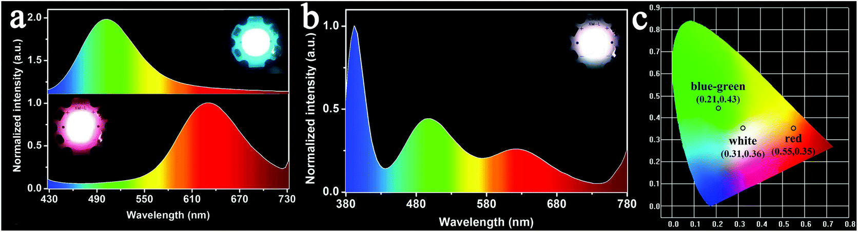 | ||
| Fig. 8 PL spectra of the LEDs on the basis of the EPD film respectively with Cu and Au sheets (a), and co-deposited film with both Au and Cu sheets (b). (c) The color coordinates of the LEDs. Insets are the optical images of the LEDs with blue-green, red, and white emission. | ||
4. Conclusion
In summary, we demonstrate the EPD of fluorescent Cu and Au sheets into film materials, which are employed to fabricate WLEDs as a color conversion layer. By studying the deposition dynamics, the factors that affect the deposition efficiency and thickness of the EPD films are well revealed. The key for governing the deposition efficiency is the lateral size of the sheets. The sheets with a large lateral size possess high electrophoretic mobility and strong face-to-face vdW interactions, thus leading to a high deposition efficiency. In our experiments, the Cu sheets have a larger lateral size than the Au sheets, so, the deposition is easier than for the Au sheets. To increase the deposition efficiency of the Au sheets, a secondary solvent with a high dielectric constant was added, which greatly enhanced the electrophoretic mobility and therefore the deposition efficiency. Such an understanding permits the adjustment of the deposition ratio of the Cu and Au sheets for tuning the emission colors of LEDs. A WLED prototype exhibits the color coordinates (x, y) = (0.31, 0.36), color temperature of 6577 K, and CRI of 88. The current work gives hope for fabricating complicated films from functional 2D nanomaterials via electrophoretic deposition.Acknowledgements
This work was supported by the NSFC (51425303, 21374042, 21174051), the 973 Program of China (2014CB643503), the Natural Science Foundation of Jilin Province (20140101048JC), the Special Project from MOST of China, and the Fundamental Research Funds for the Central Universities.References
- J. N. Coleman, M. Lotya, A. O'Neill, S. D. Bergin, P. J. King, U. Khan, K. Young, A. Gaucher, S. De, R. J. Smith, I. V. Shvets, S. K. Arora, G. Stanton, H. Y. Kim, K. Lee, G. T. Kim, G. S. Duesberg, T. Hallam, J. J. Boland, J. J. Wang, J. F. Donegan, J. C. Grunlan, G. Moriarty, A. Shmeliov, R. J. Nicholls, J. M. Perkins, E. M. Grieveson, K. Theuwissen, D. W. McComb, P. D. Nellist and V. Nicolosi, Science, 2011, 331, 568–571 CrossRef CAS PubMed.
- X. Zhang and Y. Xie, Chem. Soc. Rev., 2013, 42, 8187–8199 RSC.
- B. Dubertret, T. Heine and M. Terrones, Acc. Chem. Res., 2015, 48, 1–2 CrossRef CAS PubMed.
- X. J. Wan, Y. Huang and Y. S. Chen, Acc. Chem. Res., 2012, 45, 598–607 CrossRef CAS PubMed.
- Y. Zhu, S. Murali, M. D. Stoller, K. J. Ganesh, W. Cai, P. J. Ferreira, A. Pirkle, R. M. Wallace, K. A. Cychosz, M. Thommes, D. Su, E. A. Stach and R. S. Ruoff, Science, 2011, 332, 1537–1541 CrossRef CAS PubMed.
- J. Feng, X. Sun, C. Wu, L. Peng, C. Lin, S. Hu, J. Yang and Y. Xie, J. Am. Chem. Soc., 2011, 133, 17832–17838 CrossRef CAS PubMed.
- K. Chang and W. Chen, ACS Nano, 2011, 5, 4720–4728 CrossRef CAS PubMed.
- Q. H. Wang, K. Kalantar-Zadeh, A. Kis, J. N. Coleman and M. S. Strano, Nat. Nanotechnol., 2012, 7, 699–712 CrossRef CAS PubMed.
- S. Ithurria, M. D. Tessier, B. Mahler, R. P. S. M. Lobo, B. Dubertret and A. L. Efros, Nat. Mater., 2011, 10, 936–941 CrossRef CAS PubMed.
- X. Huang, S. Tang, X. Mu, Y. Dai, G. Chen, Z. Zhou, F. Ruan, Z. Yang and N. Zheng, Nat. Nanotechnol., 2011, 6, 28–32 CrossRef CAS PubMed.
- Y. Hernandez, V. Nicolosi, M. Lotya, F. M. Blighe, Z. Sun, S. De, I. T. McGovern, B. Holland, M. Byrne, Y. K. Gun'Ko, J. J. Boland, P. Niraj, G. Duesberg, S. Krishnamurthy, R. Goodhue, J. Hutchison, V. Scardaci, A. C. Ferrari and J. N. Coleman, Nat. Nanotechnol., 2008, 3, 563–568 CrossRef CAS PubMed.
- P. Kissel, R. Erni, W. B. Schweizer, M. D. Rossell, B. T. King, T. Bauer, S. Götzinger, A. D. Schlüter and J. Sakamoto, Nat. Chem., 2012, 4, 287–291 CrossRef CAS PubMed.
- J. W. Colson and W. R. Dichtel, Nat. Chem., 2013, 5, 453–465 CrossRef CAS PubMed.
- D. Golberg, Y. Bando, Y. Huang, T. Terao, M. Mitome, C. Tang and C. Zhi, ACS Nano, 2010, 4, 2979–2993 CrossRef CAS PubMed.
- M. Chhowalla, H. S. Shin, G. Eda, L. J. Li, K. P. Loh and H. Zhang, Nat. Chem., 2013, 5, 263–275 CrossRef PubMed.
- J. W. Seo, Y. W. Jun, S. W. Park, H. Nah, T. Moon, B. Park, J. G. Kim, Y. J. Kim and J. Cheon, Angew. Chem., Int. Ed., 2007, 46, 8828–8831 CrossRef CAS PubMed.
- C. C. Coleman, H. Goldwhite and W. Tikkanen, Chem. Mater., 1998, 10, 2794–2800 CrossRef CAS.
- M. Osada and T. Sasaki, J. Mater. Chem., 2009, 19, 2503–2511 RSC.
- R. Ma and T. Sasaki, Adv. Mater., 2010, 22, 5082–5104 CrossRef CAS PubMed.
- J. S. Son, K. Park, S. G. Kwon, J. Yang, M. K. Choi, J. Kim, J. H. Yu, J. Joo and T. Hyeon, Small, 2012, 8, 2394–2402 CrossRef CAS PubMed.
- Z. Li and X. Peng, J. Am. Chem. Soc., 2011, 133, 6578–6586 CrossRef CAS PubMed.
- L. Biadala, F. Liu, M. D. Tessier, D. R. Yakovlev, B. Dubertret and M. Bayer, Nano Lett., 2014, 14, 1134–1139 CrossRef CAS PubMed.
- J. Joo, J. S. Son, S. G. Kwon, J. H. Yu and T. Hyeon, J. Am. Chem. Soc., 2006, 128, 5632–5633 CrossRef CAS PubMed.
- J. S. Son, X. D. Wen, J. Joo, J. Chae, S. I. Baek, K. Park, J. H. Kim, K. An, J. H. Yu, S. G. Kwon, S. H. Choi, Z. Wang, Y. W. Kim, Y. Kuk, R. Hoffmann and T. Hyeon, Angew. Chem., Int. Ed., 2009, 48, 6861–6864 CrossRef CAS PubMed.
- S. R. Tamalampudi, Y. Y. Lu, U. R. Kumar, R. Sankar, C. D. Liao, B. K. Moorthy, C. H. Cheng, F. C. Chou and Y. T. Chen, Nano Lett., 2014, 14, 2800–2806 CrossRef CAS PubMed.
- S. Acharya, M. Dutta, S. Sarkar, D. Basak, S. Chakraborty and N. Pradhan, Chem. Mater., 2012, 24, 1779–1785 CrossRef CAS.
- D. Kong, W. Dang, J. J. Cha, H. Li, S. Meister, H. Peng, Z. Liu and Y. Cui, Nano Lett., 2010, 10, 2245–2250 CrossRef CAS PubMed.
- X. Tang, W. Xie, H. Li, W. Zhao, Q. Zhang and M. Niino, Appl. Phys. Lett., 2007, 90, 012102 CrossRef.
- Z. Wu, J. Liu, Y. Gao, H. Liu, T. Li, H. Zou, Z. Wang, K. Zhang, Y. Wang, H. Zhang and B. Yang, J. Am. Chem. Soc., 2015, 137, 12906–12913 CrossRef CAS PubMed.
- Z. Wu, J. Liu, Y. Li, Z. Cheng, T. Li, H. Zhang, Z. Lu and B. Yang, ACS Nano, 2015, 9, 6315–6323 CrossRef CAS PubMed.
- F. Wang, X. Zhang, Z. Zhang and C. He, J. Mater. Chem., 2011, 21, 15167–15170 RSC.
- Z. Tang, Z. Zhang, Y. Wang, S. C. Glotzer and N. A. Kotov, Science, 2006, 314, 274–278 CrossRef CAS PubMed.
- C. Schliehe, B. H. Juarez, M. Pelletier, S. Jander, D. Greshnykh, M. Nagel, A. Meyer, S. Foerster, A. Kornowski, C. Klinke and H. Weller, Science, 2010, 329, 550–553 CrossRef CAS PubMed.
- W. Cheng, M. J. Campolongo, J. J. Cha, S. J. Tan, C. C. Umbach, D. A. Muller and D. Luo, Nat. Mater., 2009, 8, 519–525 CrossRef CAS PubMed.
- T. Niu, Y. Gu and J. Huang, J. Mater. Chem., 2011, 21, 651–656 RSC.
- K. C. Ng, I. B. Udagedara, I. D. Rukhlenko, Y. Chen, Y. Tang, M. Premaratne and W. Cheng, ACS Nano, 2012, 6, 925–934 CrossRef CAS PubMed.
- M. A. Bizeto, A. L. Shiguihara and V. R. L. Constantino, J. Mater. Chem., 2009, 19, 2512–2525 RSC.
- X. Hong, C. Tan, J. Liu, J. Yang, X.-J. Wu, Z. Fan, Z. Luo, J. Chen, X. Zhang, B. Chen and H. Zhang, J. Am. Chem. Soc., 2015, 137, 1444–1447 CrossRef CAS PubMed.
- R. Jin, Nanoscale, 2015, 7, 1549–1565 RSC.
- Z. Luo, V. Nachammai, B. Zhang, N. Yan, D. T. Leong, D. E. Jiang and J. Xie, J. Am. Chem. Soc., 2014, 136, 10577–10580 CrossRef CAS PubMed.
- B. Niesen and B. P. Rand, Adv. Mater., 2014, 26, 1446–1449 CrossRef CAS PubMed.
- G. K. Mor, K. Shankar, M. Paulose, O. K. Varghese and C. A. Grimes, Nano Lett., 2006, 6, 215–218 CrossRef CAS PubMed.
- W. Ma, C. Yang, X. Gong, K. Lee and A. J. Heeger, Adv. Funct. Mater., 2005, 15, 1617–1622 CrossRef CAS.
- Z. Yin, J. Zhu, Q. He, X. Cao, C. Tan, H. Chen, Q. Yan and H. Zhang, Adv. Energy Mater., 2014, 4, 1300574 Search PubMed.
- I. Corni, M. P. Ryan and A. R. Boccaccini, J. Eur. Ceram. Soc., 2008, 28, 1353–1367 CrossRef CAS.
- L. Oakes, A. Westover, M. Mahjouri-Samani, S. Chatterjee, A. A. Puretzky, C. Rouleau, D. B. Geohegan and C. L. Pint, ACS Appl. Mater. Interfaces, 2013, 5, 13153–13160 CAS.
- Z. Niu, J. Chen, H. H. Hng, J. Ma and X. Chen, Adv. Mater., 2012, 24, 4144–4150 CrossRef CAS PubMed.
- I. Hod, W. Bury, D. M. Karlin, P. Deria, C.-W. Kung, M. J. Katz, M. So, B. Klahr, D. Jin, Y. W. Chung, T. W. Odom, O. K. Farha and J. T. Hupp, Adv. Mater., 2014, 26, 6295–6300 CrossRef CAS PubMed.
- A. R. Boccaccini, J. Cho, J. A. Roether, B. J. C. Thomas, E. Jane Minay and M. S. P. Shaffer, Carbon, 2006, 44, 3149–3160 CrossRef CAS.
- K. W. Song, R. Costi and V. Bulovic, Adv. Mater., 2013, 25, 1420–1423 CrossRef CAS PubMed.
- A. Salant, M. Shalom, I. Hod, A. Faust, A. Zaban and U. Banin, ACS Nano, 2010, 4, 5962–5968 CrossRef CAS PubMed.
- P. K. Santra and P. V. Kamat, J. Am. Chem. Soc., 2013, 135, 877–885 CrossRef CAS PubMed.
- F. Ma, S. Wang, L. Smith and N. Wu, Adv. Funct. Mater., 2012, 22, 4334–4343 CrossRef CAS.
- Z. Fu, P. M. Vilarinho, A. Wu and A. I. Kingon, Adv. Funct. Mater., 2009, 19, 1071–1081 CrossRef CAS.
- O. O. Otelaja, D. H. Ha, T. Ly, H. Zhang and R. D. Robinson, ACS Appl. Mater. Interfaces, 2014, 6, 18911–18920 CAS.
- L. Oakes, T. Hanken, R. Carter, W. Yates and C. L. Pint, ACS Appl. Mater. Interfaces, 2015, 7, 14201–14210 CAS.
- L. Oakes, D. Zulkifli, H. Azmi, K. Share, T. Hanken, R. Carter and C. L. Pint, J. Electrochem. Soc., 2015, 162, D3063–D3070 CrossRef CAS.
- J. D. Bass, X. Ai, A. Bagabas, P. M. Rice, T. Topuria, J. C. Scott, F. H. Alharbi, H. C. Kim, Q. Song and R. D. Miller, Angew. Chem., Int. Ed., 2011, 50, 6538–6542 CrossRef CAS PubMed.
- E. Lhuillier, P. Hease, S. Ithurria and B. Dubertret, Chem. Mater., 2014, 26, 4514–4520 CrossRef CAS.
- T. H. Lin, W. H. Huang, I. K. Jun and P. Jiang, Chem. Mater., 2009, 21, 2039–2044 CrossRef CAS.
- Z. S. Wu, S. Pei, W. Ren, D. Tang, L. Gao, B. Liu, F. Li, C. Liu and H. M. Cheng, Adv. Mater., 2009, 21, 1756–1760 CrossRef CAS.
- A. Chavez-Valdez, M. S. P. Shaffer and A. R. Boccaccini, J. Phys. Chem. B, 2013, 117, 1502–1515 CrossRef CAS PubMed.
- K. Roy, M. Padmanabhan, S. Goswami, T. P. Sai, G. Ramalingam, S. Raghavan and A. Ghosh, Nat. Nanotechnol., 2013, 8, 826–830 CrossRef CAS PubMed.
- J. Y. Lin, C. Y. Chan and S. W. Chou, Chem. Commun., 2013, 49, 1440–1442 RSC.
- Y. Liu, Y. Zhao, L. Jiao and J. Chen, J. Mater. Chem. A, 2014, 2, 13109–13115 CAS.
- B. Neirinck, O. Van der Biest and J. Vleugels, J. Phys. Chem. B, 2013, 117, 1516–1526 CrossRef CAS PubMed.
- H. K. Park, J. H. Oh, H. Kang, J. Zhang and Y. R. Do, ACS Appl. Mater. Interfaces, 2015, 7, 4549–4559 CAS.
- J. Ziegler, S. Xu, E. Kucur, F. Meister, M. Batentschuk, F. Gindele and T. Nann, Adv. Mater., 2008, 20, 4068–4073 CrossRef CAS.
- D. Zhou, M. Liu, M. Lin, X. Bu, X. Luo, H. Zhang and B. Yang, ACS Nano, 2014, 8, 10569–10581 CrossRef CAS PubMed.
Footnote |
| † Electronic supplementary information (ESI) available: Additional experimental information, and SEM images of Cu EPD films. See DOI: 10.1039/c5nr06599b |
| This journal is © The Royal Society of Chemistry 2016 |