
Epitaxial patterning of nanometer-thick Y3Fe5O12 films with low magnetic damping
Shaozhen
Li†
*ab,
Wei
Zhang†
a,
Junjia
Ding†
a,
John E.
Pearson
a,
Valentine
Novosad
a and
Axel
Hoffmann
a
aMaterials Science Division, Argonne National Laboratory, Argonne, IL 60439, USA
bSchool of Physics and Institute for Quantum Materials, Hubei Polytechnic University, Huangshi 435003, P. R. China. E-mail: shaozhenli@yahoo.com
First published on 27th November 2015
Abstract
Magnetic insulators such as yttrium iron garnet, Y3Fe5O12, with extremely low magnetic damping have opened the door for low power spin–orbitronics due to their low energy dissipation and efficient spin current generation and transmission. We demonstrate here reliable and efficient epitaxial growth and nanopatterning of Y3Fe5O12 thin-film based nanostructures on insulating Gd3Ga5O12 substrates. In particular, our fabrication process is compatible with conventional sputtering and lift-off, and does not require aggressive ion milling which may be detrimental to the oxide thin films. Their structural and magnetic properties indicate good qualities, in particular low magnetic damping of both films and patterned structures. The dynamic magnetic properties of the nanostructures are systematically investigated as a function of the lateral dimension. By comparing with ferromagnetic nanowire structures, a distinct edge mode in addition to the main mode is identified by both experiments and simulations, which also exhibit cross-over with the main mode upon varying the width of the wires. The non-linear evolution of dynamic modes over nanostructural dimensions highlights the important role of size confinement to their material properties in magnetic devices where Y3Fe5O12 nanostructures serve as the key functional component.
1. Introduction
Magnetic insulators such as yttrium iron garnet, Y3Fe5O12 (YIG) with extremely low magnetic damping have been indispensable in almost every aspect of contemporary spin–orbitronics research.1,2 For many decades, the growth of single crystal YIG films has been dominated by liquid phase epitaxy (LPE),3 which yields films in the thickness range from several hundreds of nanometers to millimeters. On the other hand, the exotic magnetic properties revealed recently for various YIG-based magnetic heterostructures4–8 call for an urgent need for their nanostructured forms in order to realize practical devices for applications, including spin transfer torque devices,9–11 magnetic logic devices,12,13 auto-oscillators,9,14 and skyrmion memory.15 However, the conventional LPE method is incompatible with current industrial top-down nanofabrication technologies. Recently, great advances have been achieved in the growth of high quality YIG films using pulsed laser deposition (PLD) and magnetron sputtering at elevated temperatures,16–22 yielding nanometer-thick films with low magnetic damping similar to single-crystal YIG bulk materials. For example, a Gilbert damping constant of α = 0.00023 has been achieved by Sun et al.16 and by d'Allivy Kelly et al.17 using PLD, and α ∼ 0.00009 has been achieved by Chang et al.19 using magnetron sputtering. These demonstrations, more suited for commercial production, are of great technological significance.Despite the intensive investigations on YIG continuous films, an efficient yet reliable method for epitaxial patterning of YIG nanostructures is still missing. Microstructured YIG films have been prepared in the past using aggressive ion etching of sputtered YIG films while using resist masks to define the morphological structures.9,23,24 However, the injected, highly energized Ar ions are also detrimental to the films, particularly harmful to oxides with higher stiffness as opposed to metals.25 Mechanical defects and even cracks, as well as non-trivial modifications of the magnetic properties such as saturation magnetization and damping constant have been observed after the ion milling process.24 In this work, we report high-quality growth of YIG films using combined room temperature (RT) magnetron sputtering and ex situ post annealing. In particular, our approach is also compatible with modern nano-lithography techniques, taking advantage of the RT deposition. We demonstrate epitaxial patterned YIG nanostructures using electron beam lithography and lift-off. A Gilbert damping constant comparable to the extended thin-films is achieved even for the patterned structures.
2. Results and discussion
The YIG films are deposited on (111)-oriented gadolinium gallium garnet (Gd3Ga5O12, GGG) single crystal substrates at room temperature (RT) from a commercial YIG sputter target. The Ar gas flow, chamber pressure, and sputtering power are kept at 16 sccm, 10 mT, and 75 W, respectively, which is the optimal deposition environment for RT growth. It has been shown previously that these films can display different surface morphologies26 depending on the growth conditions. Here, we used very low sputtering rate and deposited our films from a stoichiometric YIG target under ultrahigh vacuum. In addition, our sputtering system has an on-axis geometry which does not induce any substrate misorientation. The as-grown films have a dark gray color implying that the stoichiometry has changed during the RT deposition. The films are subsequently subjected to an ex situ post annealing at 800 °C for 2 hours in a tube furnace with continuous air flow. The temperature ramping rate is ∼120 °C per hour. The key attributes for obtaining a good film in our process is to ensure an oxygen-rich environment during annealing. Nevertheless, we found that flowing just air at ambient pressure is sufficient enough instead of using pure oxygen. Alternatively, such annealing can also be done in situ after the film growth;18 however, much longer annealing time (>10 hours) is required primarily due to the limitation of the maximum achievable oxygen partial pressure in the commercial sputtering chamber. The annealed films have a light yellow color (nanometer-thick YIG films).Nanostructured YIG films are fabricated by RT deposition onto PMMA/PMGI bilayer resists defined via electron beam lithography (Raith 150). Since the GGG substrate is highly insulating, we sputtered 5 nm-thick Au after spin coating the bilayer resists to allow efficient electron charge dissipation during the lithography. The Au layer is subsequently removed by using a gold etcher, followed by wet development of PMMA (MicroChem MIBK) and PMGI (Shipley CD-26), respectively. The PMMA/PMGI bilayer resists can form an undercut cross-section profile which is suitable for magnetron sputtering deposition. After the deposition of 40 nm YIG film using the same procedure as before, we remove the resists and surplus materials on top by using a resist remover (Shipley 1165). Finally, the nanostructured samples are annealed using the same procedure as for continuous films. Although we choose to use electron beam lithography for our demonstration, the general process is also applicable to other unconventional lithography techniques.27
We first characterized our YIG films structurally and magnetically. Fig. 1(a) and (b) show the X-ray diffraction patterns of our YIG films. The data confirm the (111)-oriented YIG phase in the samples and show no evidence of the existence of any additional phases. Fig. 1(c) shows the magnetic hysteresis loop measured by a vibrating sample magnetometry with an in-plane magnetic field. The data indicates very small coercivity, below 1 Oe, and a saturation magnetization, Ms = 130 ± 20 emu cm−3. This value is equivalent to a 4πMs = 1633 ± 251 G, which is only 6% smaller than the literature value for bulk YIG crystals.1 A more precise value of 4πMs will be determined via dynamic measurements below.
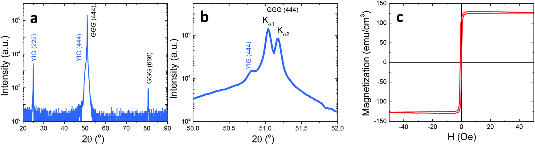 | ||
| Fig. 1 (a) X-ray diffraction pattern of a 40 nm annealed YIG film, and (b) the same spectrum in a magnified scale showing the YIG(444) peak. (c) Magnetic hysteresis loop of the same sample measured with an in-plane magnetic field, yielding a saturation magnetization value of ∼130 emu cm−3. | ||
Dynamic magnetic properties are investigated by a vector-network-analyzer ferromagnetic-resonance method (VNA-FMR) in a probe station using low-loss rf probes. We prepared 18 μm × 2 mm large YIG bars using the previously described patterning method. Considering that the thickness of the YIG film is only 40 nm, these structures are large enough to be considered as continuous films, which also serve as the reference samples for our YIG nanostructures as will be discussed later. On chip coplanar-waveguides made from Ti(5 nm)/Au(150 nm) are subsequently fabricated on top of the YIG bars by photolithography and lift-off methods. The measurement configuration is illustrated in Fig. 2(a). We show in Fig. 2(b) and (c) the ferromagnetic resonance data of three different YIG samples (Fm1,2,3, where Fm denotes ‘Film’). The resonance field, HFMR, versus frequency, f, can be fitted by the Kittel equation:
 | (1) |
 | (2) |
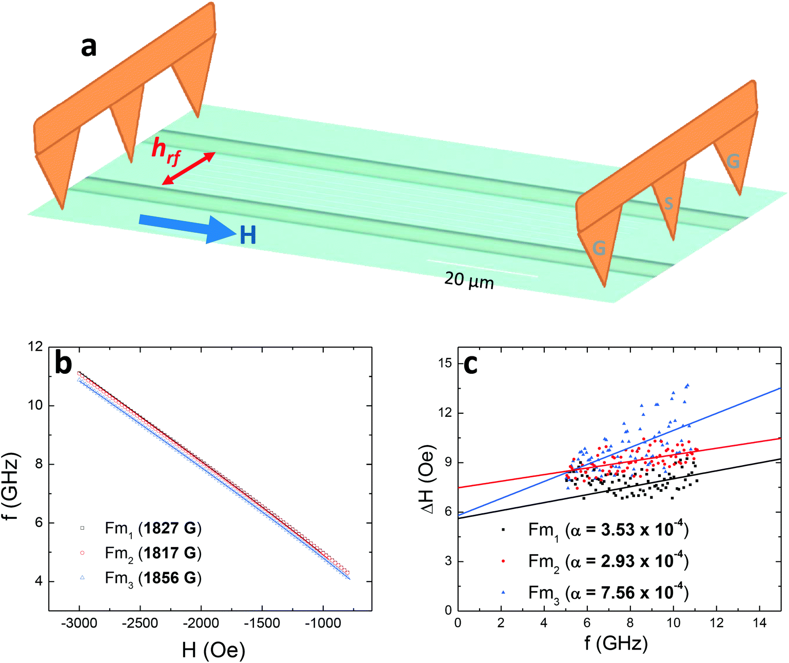 | ||
| Fig. 2 (a) VNA-FMR measurement configuration showing the directions of static and dynamic magnetic fields with respect to the samples. Ferromagnetic resonance data of three YIG large bars (Fm1,2,3) showing (b) resonance frequency versus field and the corresponding fitting with the Kittel equation, and (c) resonance linewidth versus frequency and the corresponding linear fitting. | ||
We next move onto the discussions of nanostructured YIG. We prepared arrays of YIG nanowires (NW), and nanodots (ND) with varying dimensions using the previously described method. Owing to the top-down lithography used here, all nanostructures exhibit quite uniform size and spacing.29 As a demonstration, we fabricated NW samples with different widths, denoted as NW300,450,600,750,1800, where the subscript indicates the wire width in nanometers. We also prepared circular and elliptical dots of similar dimensions. Fig. 3 shows the morphology of our nanostructured YIG samples by using scanning electron microscopy after 5 nm Au coating. Clean edges and faithful pattern transfer are achieved thanks to the well-defined undercut resist bilayer. The morphology of these patterned films is also similar to their continuous-film counterparts due to the identical growth and annealing conditions.
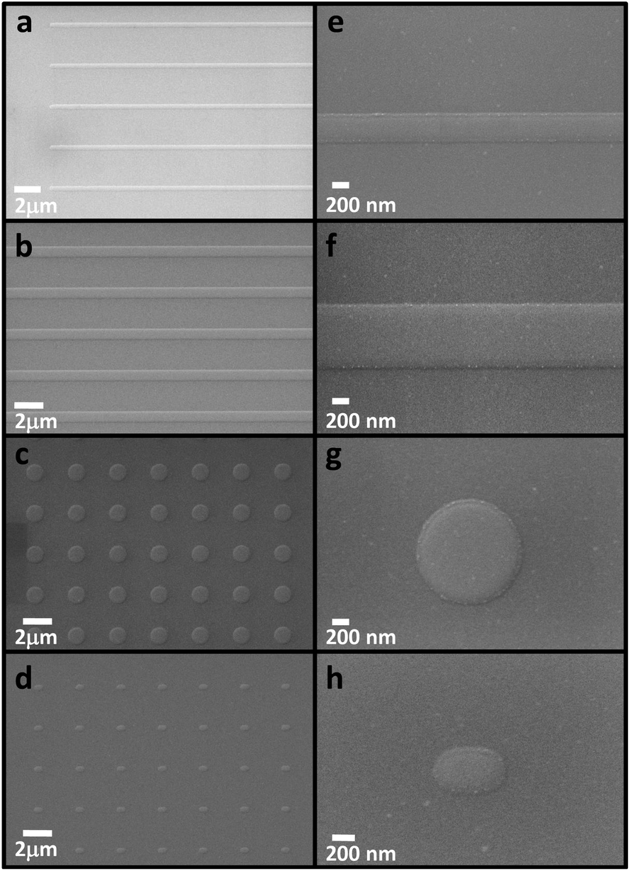 | ||
| Fig. 3 Scanning electron microscopy images of epitaxial patterned YIG nanostructures on GGG substrates showing (a) 300 nm-wide wires, (b) 750 nm-wide wires, (c) 600 nm-radius circular dots, (d) 410 nm × 670 nm elliptical dots, and their corresponding zoomed-in images (e–h). | ||
We fabricated on-chip coplanar waveguides on top of each patterned arrays in order to study the dynamic properties of nanostructured YIG. We focus primarily on the NW samples with varying widths so that the effects of geometrical confinement to the magnetization dynamics can be systematically investigated. The gray scale mapping in Fig. 4(a) and (b) compare the FMR properties of Fm1 and NW300. The bright color indicates low microwave absorption, while the dark color corresponds to high microwave absorption. The FMR spectrum of the continuous film is symmetric, while the spectrum of NW300 exhibits a clear asymmetry with respect to H = 0 due to the shape anisotropy that originated from the confined edges of the nanostructures. In addition to the main FMR mode, we clearly identify an appreciable edge mode for the NW300 sample. Both the main and edge modes are accurately reproduced by our micromagnetic simulations using a MuMax Simulator,30 see Fig. 4(c) and (d). The parameters used for the simulation are: Ms = 147.77 emu cm−3, Aex = 4 × 10⁻¹³ J m−1, α = 7.561 × 10⁻⁴, γ = 0.00284 GHz Oe−1. All the values are based on the fitting results of the reference sample. At H = −1000 Oe, the simulated edge mode is at ∼5.5 GHz [Fig. 4(d)], which agrees very well with the experiment.
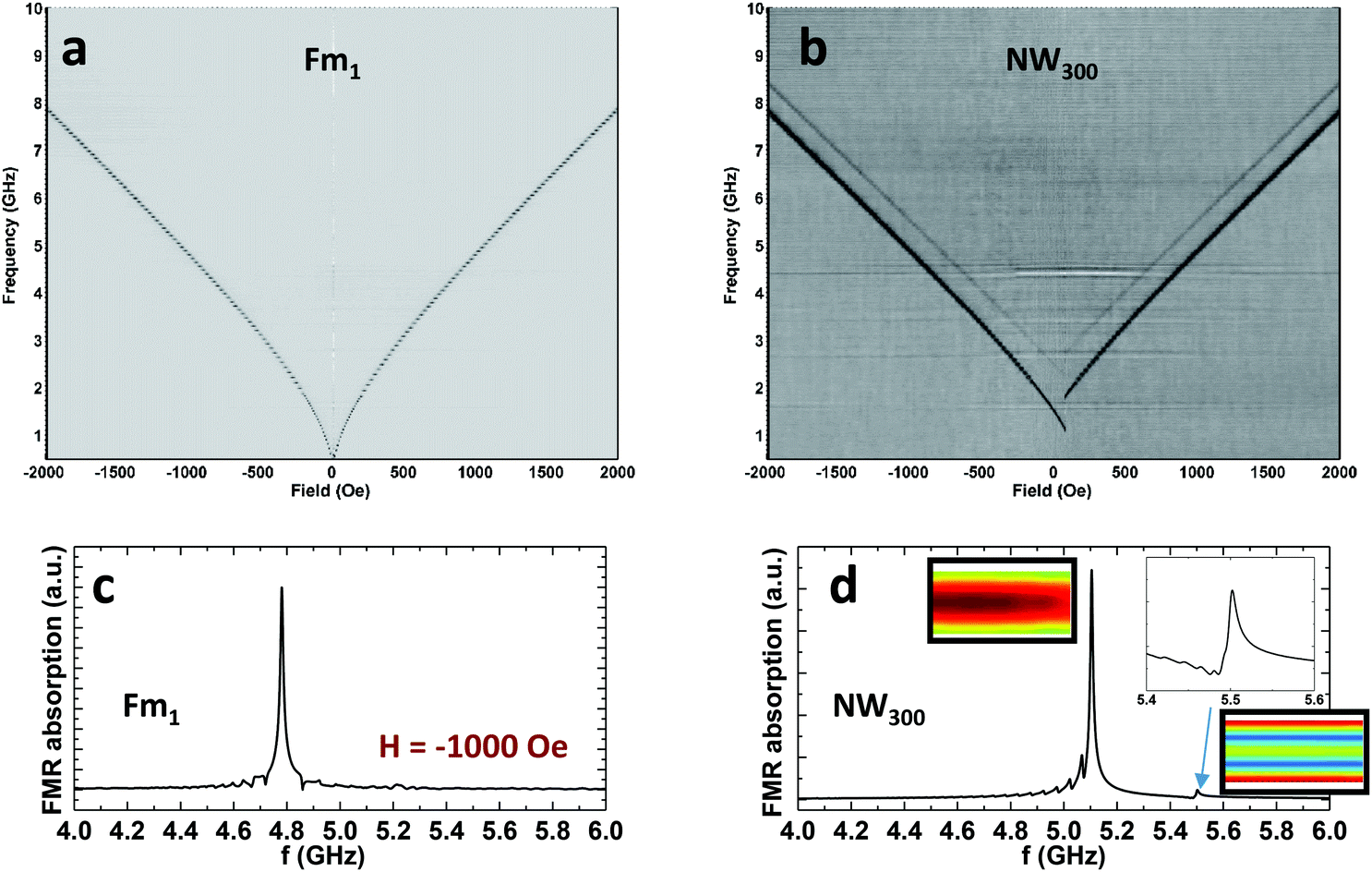 | ||
| Fig. 4 FMR 2D-spectrum recorded for samples (a) Fm1 and (b) NW300, and the corresponding micromagnetic simulations at H = −1000 Oe (c and d). Both main and edge modes are identified for NW300. The inset pictures of (d) show simulated spatial distribution of magnetization dynamics from the two modes, in which the red color indicates high spin precession amplitude, and the blue color corresponds to low amplitude. | ||
Edge modes can be expected for generic nanopatterned magnetic films. However, earlier work has shown that such modes are missing in high damping ferromagnetic metals such as Permalloy (Py, Ni80Fe20) nanowires with similar structural dimensions.31 The distinct edge modes of YIG nanostructures observed here is owing to the intrinsic low magnetic damping and weak magnon exchange interactions of YIG, so that they can be well separated from the main FMR mode.
Fig. 5 further demonstrates the evolution of such edge mode with the width of the nanowires. Starting from NW300, the edge mode moves closer for NW450 as the width increases, and finally merges with the main FMR mode for NW600. Notably, this mode starts to reoccur for NW750 and NW1800 as the width further increases. This cross-over between main and edge modes indicates a higher sensitivity of the edge mode than the main mode to the change of local demagnetization field since they reside primarily at the edges of the nanowires where the pinning is much stronger as opposed to the center [Fig. 4(d)]. The strong demagnetization field is also evidenced by the fact that even the main mode shows clear evolution with width at H = 0 Oe, as shown in Fig. 6(a) and (b). However, when the external field is sufficiently high, no appreciable evolution with width can be observed for the main mode, Fig. 6(b).
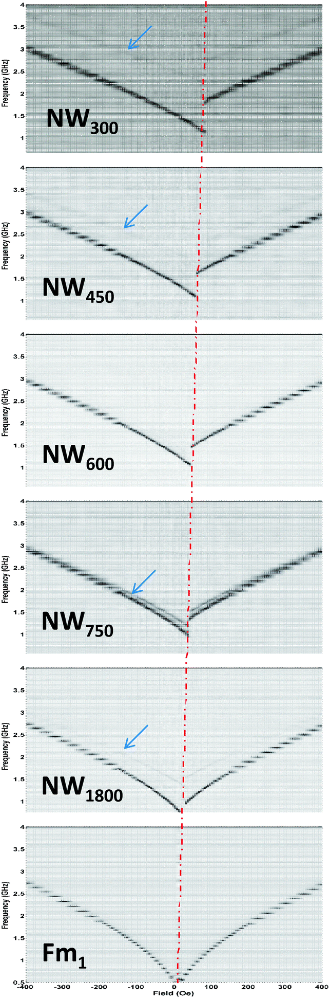 | ||
| Fig. 5 FMR 2D-spectrum of Fm1 and NW series of samples, showing evolution of the coercivity (dashed line) and the magnetization dynamic modes over the width of the wires. Arrows indicate the existence of edge modes. Only the ascending field branch of the hysteresis is shown for simplicity. | ||
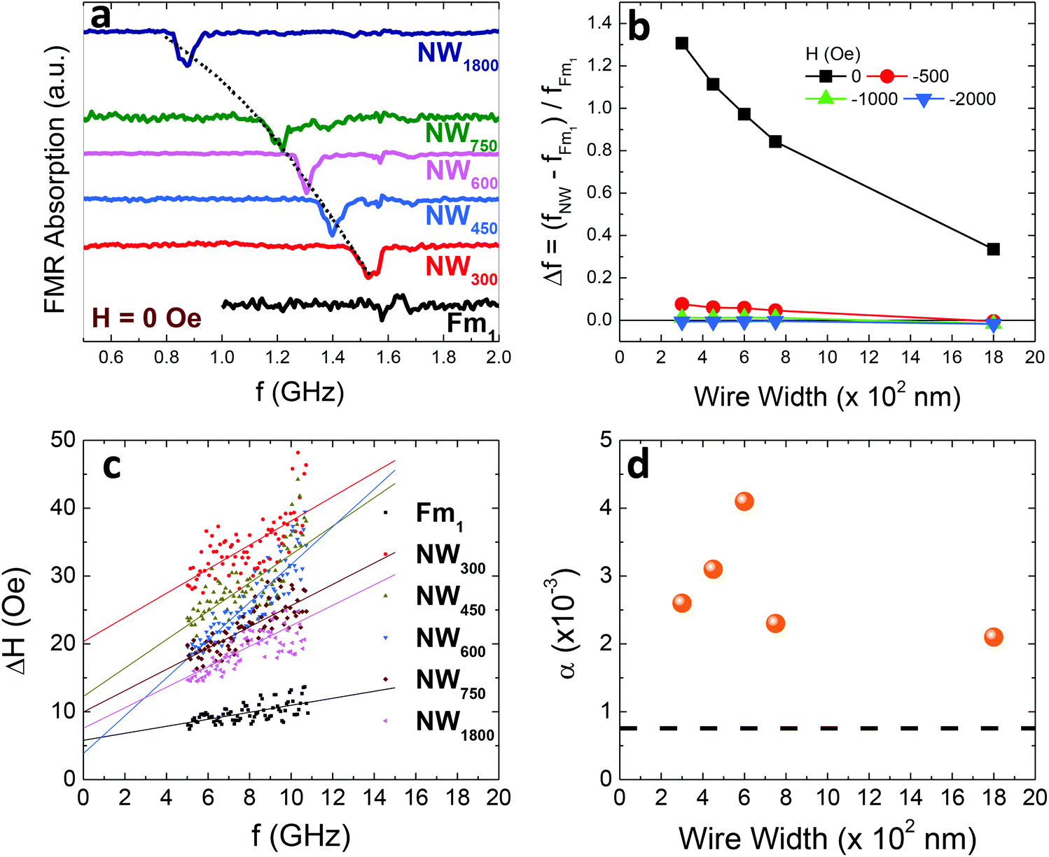 | ||
| Fig. 6 (a) FMR 1D-spectrum of Fm1 and NW series samples recorded at zero external field showing the evolution of the main FMR mode. (b) Percentage change in the resonance frequency of the main FMR mode at different external applied fields, H = 0, −500, −1000, and −2000 Oe for different widths of the nanowire. (c) Resonance linewidth versus frequency of the different samples. (d) Extracted magnetic damping values for nanowires with different widths. Dashed line indicates the damping value for the continuous film. | ||
The ‘appear–merge–reoccur’ behavior of the edge mode to the main mode (Fig. 5) is an interesting observation, which also finds good agreement with the evolution of the damping constant. We study the frequency dependent resonance linewidth for all our NW samples [Fig. 6(c)] and extract the damping parameters via fitting with eqn (2), as shown in Fig. 6(d). Starting from NW300, the damping constant increases as width increases, and peaks at NW600, corresponding to exactly the merge point of the edge and main modes in Fig. 5. This is explained by the fact that when the two modes degenerate, they are coupled due to magnon–magnon scattering leading to efficient energy transfer between the modes,32 which as a result has their effective damping increased. The loss of the edge mode at this point is compensated by the large damping enhancement for the main mode. After all, it is the total linewidth that truly quantifies the loss of magnetic energy regardless of the nature and number of microscopic mechanisms involved. In fact, such degeneracy is something to be avoided for device applications such as for the magnetic auto-oscillators, because it could lead to self-limiting damping and prevent the onset of auto-oscillations. Therefore, our results here highlight the significance and general guidance of proper device engineering for YIG based spintronics.
3. Conclusions
Magnetic insulators with low magnetic damping such as Y3Fe5O12 have been widely proposed and investigated as good candidates for pure spin current spintronics concepts. Fundamental studies have reached several milestones in many sub-fields such as spin pumping, spin-Seebeck effect, spin transfer torque, and auto-oscillation. However, successful patterning of nanostructures from such materials for practical device applications has only recently become feasible.Here, we have demonstrated reliable and efficient epitaxial growth and nanopatterning of Y3Fe5O12 thin-film based nanostructures on insulating GGG substrates. Their structural and magnetic properties indicate good qualities, in particular low magnetic damping of both films and patterned structures. We systematically studied the evolution of the dynamic magnetization parameters over the change of the lateral dimensions. A distinct edge mode in addition to the main mode is identified by both experiments and simulations, which also exhibit cross-over with the main mode over changing the width of the wires. The cross-over leads to also a significantly enhanced magnetic damping. The non-linear evolution of dynamic modes over nanostructural dimensions highlights the important role of size confinement to their material properties in magnetic devices where YIG nanostructures serve as the key functional component.
Conflict of interest
The authors declare no competing financial interest.Acknowledgements
We thank Dr Jennifer Zheng and Dr Junjie Zhang for technical help for using the tube furnace. Work at Argonne was supported by the U.S. Department of Energy, Office of Science, Materials Science and Engineering Division. Use of the Center for Nanoscale Materials was supported by the U.S. Department of Energy, Office of Science, Basic Energy Sciences, under contract no. DE-AC02-06CH11357. S. L. acknowledges the National Natural Science Foundation of China (no. 51302074 and 11374147), the Natural Science Foundation of Hubei Province (no. 2012FFB010), the Creative team of Hubei Polytechnic University of China (Project no. 13xtz05), and the Education Foundation of Hubei Province (D20144402).References
- Recent Advances in Magnetic Insulators – From Spintronics to Microwave Applications, in Solid State Physics, ed. M. Wu and A. Hoffmann, Academic Press, 2013, vol. 64 Search PubMed.
- A. Hoffmann and S. D. Bader, Opportunities at the frontier of spintronics, Phys. Rev. Appl., 2015, 4, 047001 CrossRef.
- R. C. M. Linares, R. B. Graw and J. B. Schroeder, Growth and Properties of Yttrium Iron Garnet Single Crystal Films, J. Appl. Phys., 1965, 36, 2884 CrossRef CAS.
- Y. Kajiwara, K. Harii, S. Takahashi, J. Ohe, K. Uchida, M. Mizuguchi, H. Umezawa, H. Kawai, K. Ando, K. Takanashi, S. Maekawa and E. Saitoh, Transmission of electrical signals by spin-wave interconversion in a magnetic insulator, Nature, 2010, 464, 262 CrossRef CAS PubMed.
- B. Heinrich, C. Burrowes, E. Montoya, B. Kardasz, E. Girt, Y. Y. Song, Y. Sun and M. Wu, Spin Pumping at the Magnetic Insulator (YIG)/Normal Metal (Au) Interfaces, Phys. Rev. Lett., 2010, 107, 066604 CrossRef PubMed.
- A. V. Chumak, A. A. Serga and B. Hillebrands, Magnon transistor for all-magnon data processing, Nat. Commun., 2014, 5, 4700 CrossRef CAS PubMed.
- D. Qu, S. Y. Huang, J. Hu, R. Wu and C. L. Chien, Intrinsic Spin Seebeck Effect in Au/YIG, Phys. Rev. Lett., 2013, 110, 067206 CrossRef CAS PubMed.
- H. Nakayama, M. Althammer, Y. T. Chen, K. Uchida, Y. Kajiwara, D. Kikuchi, Y. Ohtani, S. Geprags, M. Opel, S. Takahashi, R. Gross, G. E. W. Bauer, S. T. B. Goennenwein and E. Saitoh, Spin Hall Magnetoresistance Induced by a Nonequilibrium Proximity Effect, Phys. Rev. Lett., 2013, 110, 206601 CrossRef CAS PubMed.
- A. Hamadeh, O. d'Allivy Kelly, C. Hahn, H. Meley, R. Bernard, A. H. Molpeceres, V. V. Naletov, M. Viret, A. Anane, V. Cros, S. O. Demokritov, J. L. Prieto, M. Munoz, G. de Loubens and O. Klein, Full Control of the Spin-Wave Damping in a Magnetic Insulator Using Spin–Orbit Torque, Phys. Rev. Lett., 2014, 113, 197203 CrossRef CAS PubMed.
- J. Sklenar, et al., Driving and detecting ferromagnetic resonance in insulators with the spin Hall effect, Phys. Rev. B: Condens. Matter Mater. Phys., 2015, 92, 174406 CrossRef.
- M. B. Jungfleisch, et al., Large spin-wave bullet in a ferrimagnetic insulator driven by spin Hall effect, 2015, arXiv:1505.07791.
- A. V. Chumak, V. I. Vasyuchka, A. A. Serga and B. Hillebrands, Magnon spintronics, Nat. Phys., 2015, 11, 453461 CrossRef.
- J. Ding, M. Kostylev and A. O. Adeyeye, Realization of a mesoscopic reprogrammable magnetic logic based on a nanoscale reconfigurable magnonic crystal, Appl. Phys. Lett., 2012, 100, 073114 CrossRef.
- V. E. Demidov, S. Urazhdin, H. Ulrichs, V. Tiberkevich, A. Slavin, D. Baither, G. Schmitz and S. O. Demokritov, Magnetic nano-oscillator driven by pure spin current, Nat. Mater., 2012, 11, 1028–1031 CAS.
- W. Jiang, P. Upadhyaya, W. Zhang, Q. Yu, M. B. Jungfleisch, F. Y. Fradin, J. E. Pearson, Y. Tserkovnyak, K. L. Wang, O. Heinonen, S. G. E. te Velthuis and A. Hoffmann, Blowing magnetic skyrmion bubbles, Science, 2015, 349, 283–286 CrossRef CAS PubMed.
- Y. Sun, Y. Y. Song, H. Chang, M. Kabatek, M. Jantz, W. Schneider, M. Wu, H. Schultheiss and A. Hoffmann, Growth and ferromagnetic resonance properties of nanometer-thick yttrium iron garnet films, Appl. Phys. Lett., 2012, 101, 152405 CrossRef.
- O. d'Allivy Kelly, A. Anane, R. Bernard, J. Ben Youssef, C. Hahn, A. H. Molpeceres, C. Carretero, E. Jacquet, P. Bortolotti, R. Lebourgeois, J.-C. Mage, G. de Loubens, O. Klein, V. Cros and A. Fert, Inverse spin Hall effect in nanometer-thick yttrium iron garnet/Pt system, Appl. Phys. Lett., 2013, 103, 082408 CrossRef.
- T. Liu, H. Chang, V. Vlaminck, Y. Sun, M. Kabatek, A. Hoffmann, L. Deng and M. Wu, Ferromagnetic resonance of sputtered yttrium iron garnet nanometer films, J. Appl. Phys., 2014, 115, 17A501 CrossRef.
- H. Chang, P. Li, W. Zhang, T. Liu, A. Hoffmann, L. Deng and M. Wu, Nanometer-Thick Yttrium Iron Garnet Films With Extremely Low Damping, IEEE Magn. Lett., 2014, 5, 6700104 Search PubMed.
- H. L. Wang, C. H. Du, P. C. Hammel and F. Y. Yang, Strain-Tunable Magnetocrystalline Anisotropy in Epitaxial Y3Fe5O12 Thin Films, Phys. Rev. B: Condens. Matter Mater. Phys., 2014, 89, 134404 CrossRef.
- M. C. Onbasli, A. Kehlberger, D. H. Kim, G. Jakob, M. Klaui, A. V. Chumak, B. Hillebrands and C. A. Ross, Pulsed laser deposition of epitaxial yttrium iron garnet films with low Gilbert damping and bulk-like magnetization, APL Mater., 2014, 2, 106102 CrossRef.
- A. Kehlberger, K. Richter, M. C. Onbasli, G. Jakob, D. H. Kim, T. Goto, C. A. Ross, G. Gotz, G. Reiss, T. Kuschel and M. Klaui, Enhanced Magneto-optic Kerr Effect and Magnetic Properties of CeY2Fe5O12 Epitaxial Thin Films, Phys. Rev. Appl., 2015, 4, 014008 CrossRef.
- C. Hahn, V. V. Naletov, G. de Loubens, O. Klein, O. d'Allivy Kelly, A. Anane, R. Bernard, E. Jacquet, E. Bortolotti, V. Cros, J. L. Prieto and M. Munoz, Measurement of the intrinsic damping constant in individual nanodisks of Y3Fe5O12 and Y3Fe5O12/Pt, Appl. Phys. Lett., 2014, 104, 152410 CrossRef.
- M. B. Jungfleisch, W. Zhang, W. Jiang, H. Chang, J. Sklenar, S. M. Wu, J. E. Pearson, A. Bhattacharya, J. B. Ketterson, M. Wu and A. Hoffmann, Spin waves in micro-structured yttrium iron garnet nanometer-thick films, J. Appl. Phys., 2015, 117, 17D128 CrossRef.
- W. Zhang and K. M. Krishnan, Epitaxial patterning of thin-films: conventional lithographies and beyond, J. Micromech. Microeng., 2014, 24, 093001 CrossRef.
- I. I. Syvorotka, I. M. Syvorotka and I. V. Kityk, Surface morphological changes and magnetic properties of Sc-substituted Y3Fe5O12 epitaxial films deposited on the GGG substrate, J. Magn. Magn. Mater., 2010, 322, 3314 CrossRef CAS.
- W. Zhang, et al. , J. Appl. Phys., 2010, 107, 09D724 Search PubMed; W. Zhang, et al. , J. Appl. Phys., 2013, 113, 17B502 ( J. Micromech. Microeng. , 2011 , 21 , 045024 ) Search PubMed.
- S. S. Kalarickal, P. Krivosik, M. Wu, C. E. Patton, M. L. Schneider, P. Kabos, T. J. Silva and J. P. Nibarger, Ferromagnetic resonance linewidth in metallic thin films: Comparison of measurement methods, J. Appl. Phys., 2006, 99, 093909 CrossRef.
- A. O. Adeyeye and N. Singh, Large area patterned magnetic nanostructures, J. Phys. D: Appl. Phys., 2008, 41, 153001 CrossRef.
- A. Vansteenkiste, et al., The design and verification of MuMax3, AIP Adv., 20144, 107133 Search PubMed.
- J. Ding, M. Kostylev and A. O. Adeyeye, Magnetic hysteresis of dynamic response of one-dimensional magnonic crystals consisting of homogenous width nanowires observed with broadband ferromagnetic resonance, Phys. Rev. B: Condens. Matter Mater. Phys., 2011, 84, 054425 CrossRef.
- R. Adur, C. Du, H. Wang, S. A. Manuilov, V. P. Bhallamudi, C. Zhang, D. V. Pelekhov, F. Yang and C. P. Hammel, Damping of Confined Modes in a Ferromagnetic Thin Insulating Film: Angular Momentum Transfer across a Nanoscale Field-Defined Interface, Phys. Rev. Lett., 2014, 113, 176601 CrossRef PubMed.
Footnote |
| † These authors contributed equally to this work. |
| This journal is © The Royal Society of Chemistry 2016 |