
Dislocation-driven growth of porous CdSe nanorods from CdSe·(ethylenediamine)0.5 nanorods†
Hyung-Bae
Kim
and
Du-Jeon
Jang
*
Department of Chemistry, Seoul National University, NS60, Seoul 08826, Korea. E-mail: djjang@snu.ac.kr; Fax: +82 2 875 6624; Tel: +82 2 880 4368
First published on 18th November 2015
Abstract
Porous CdSe nanorods having a novel flute-like morphology have been prepared facilely via the hydrothermal treatment of CdSe·(en)0.5 (en = ethylenediamine) nanorods as sacrificial templates. During the hydrothermal process, various crystalline imperfections such as stacking faults and twinning planes appear due to lattice mismatches between orthorhombic CdSe·(en)0.5 and hexagonal wurtzite porous CdSe nanorods and subsequently disappear to release mismatched strains. In the self-healing process of defects, due to the imbalance of in-and-out atomic diffusion, point defects of atomic vacancies are heavily generated in CdSe nanorods to produce volume defects of voids eventually. The photoluminescence of CdSe nanorods shifts to the red region and decreases in intensity with the increase of the hydrolysis time as surface states and selenium vacancies increase. The mean lifetime of photoluminescence increases with the increase of the hydrothermal-treatment time as the fractional amplitude of the surface-state-related component increases.
Introduction
The morphology control of nanomaterials has been considered to be a crucial issue in nanotechnology research due to their structure-dependent fundamental properties.1–7 In particular, the fabrication of one dimensional (1D) nanostructures such as nanorods, nanowires, nanobelts and nanotubes has attracted considerable scientific attention owing to their novel properties in optoelectronic and electrochemical applications.8–11 Solution-phase synthetic strategies have been widely used to prepare controlled 1D semiconductor nanostructures.12 Among them, solvothermal solvent-coordination molecular template (SCMT) methods have been widely used to produce novel inorganic–organic nanostructures.12–15 Novel inorganic–organic hybrid nanomaterials of MX·(Y)n composites (M = Cd, Zn, Mn; X = S, Se, Te; Y = amine derivatives; n = 0.5 or 1) have been fabricated easily via SCMT routes.13,14,16–18 The MX·(Y)n nanomaterials have strong quantum-confinement effects and high carrier mobility owing to their layered structures. Furthermore, they have been considered as useful precursors for the production of MX semiconductor nanostructures via hydrothermal treatment.17–19 Typically, the intrinsic morphologies of MX·(Y)n nanostructures are preserved even after conversion into MX, but their structures are sometimes turned into porous structures due to the removal of organic moieties. Consequently, with the assistance of MX·(Y)n precursors, MX semiconductor nanostructures can have novel porous morphologies.13,19When crystal lattices are subjected to stress, crystal defects are often produced as a means of the energy minimization of high surface tensions. Generally, the crystal defects are classified by their dimension as point defects, line defects, planar defects, and volume defects, and these crystal imperfections can significantly affect the properties of semiconductor nanostructures.20–23 Crystal defects do not always have negative effects on the quality of nanocrystals but rather are exploitable in realizing interesting concepts such as the construction of multiquantum wells,24 the synthesis of branched nanostructures,25 and the creation of internal voids.23,26–28 1D nanostructures are prone to having planar defects such as stacking faults and twinning planes during the crystal growth.21–23 Particularly, stacking faults, which are generated between line defects, are an important class of planar defects commonly observed in closely packed crystal structures. They have been often produced at every boundary of two different crystal structures such as hexagonal wurtzite and cubic zinc-blende. Thus, stacking faults are used as internal standards for detecting orientations and phase transitions in nanostructures.21,22 Consequently, understanding the formation mechanisms of stacking faults is crucial in controlling nanostructures better via defect engineering.
CdSe, which has a narrow band gap of 1.74 eV, is one of the most attractive II–VI semiconductor materials with wide potential applications in fabricating nanoscale electronic, photonic, electromechanical, and biomedical devices.3–6,29,30 CdSe is used as an ideal system to verify the kinetic model of particle growth in solution phases, which further directs the synthesis of additional analogue II–VI semiconductor materials such as ZnS, ZnSe, CdS, and CdTe. Therefore, it is meaningful to develop new synthetic approaches to control CdSe nanostructures. Although there are numerous reports about the synthesis of 1D CdSe nanostructures, the preparation of porous 1D CdSe nanostructures has been rarely reported in spite of the importance of porous nanomaterials.31–33
Herein, we demonstrate a unique strategy to produce porous CdSe nanorods with the assistance of crystal defects. CdSe·(ethylenediamine)0.5 nanorods have been used as sacrificial templates to produce porous CdSe nanorods. During the hydrothermal transformation of CdSe·(ethylenediamine)0.5 nanorods into porous CdSe nanorods, various crystalline imperfections such as stacking faults and twinning planes have been found to appear and subsequently disappear to release mismatched strains. On the basis of our observation of the generation and disappearance of various defects, we suggest a dislocation-driven formation mechanism of porous CdSe nanorods (Fig. 1). Furthermore, we have also observed the defect-related photophysical properties of as-prepared porous CdSe nanorods. Thus, we believe that this work provides a novel strategy for the rational design of defect-engineered nanostructures.
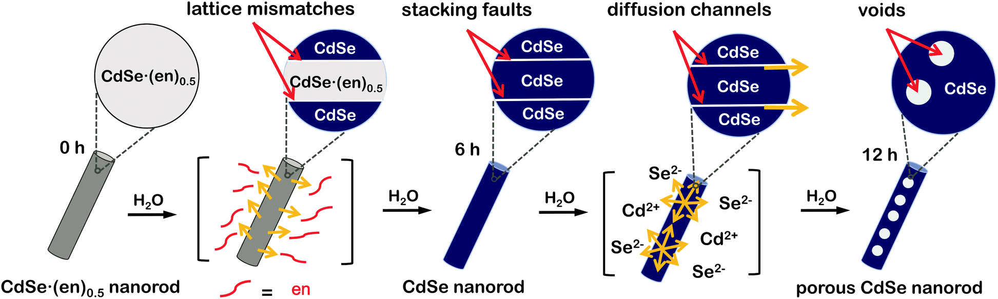 | ||
| Fig. 1 Schematic illustration of the formation of porous CdSe nanorods via the hydrothermal treatment of CdSe·(en)0.5nanorods. The formation mechanism is depicted as a function of the hydrothermal-treatment time. | ||
Experimental
Materials
The analytical grade chemicals of CdCl2(s), Se(s), ethylenediamine(l, en), and hydrazine monohydrate(l) were purchased from Sigma-Aldrich. Ultrapure deionized water (>17 MΩ cm) from a Millipore Milli-Q system was used throughout the experiments.Synthesis of CdSe·(en)0.5 nanorods
1.0 mmol of CdCl2 was put into 30 mL of en and the mixture was sonicated in an ultrasonic bath for 30 min. Then, 0.50 mmol of Se and 0.25 mmol of hydrazine monohydrate were added into the above mixture and stirred vigorously for 1 h. The mixture solution was loaded into a Teflon-lined stainless-steel autoclave of 50 mL capacity, placed in a preheated oven at 200 °C for 12 h, and cooled to room temperature naturally. A dark brown precipitate produced in the reaction mixture was washed twice with deionized water and ethanol to remove residual impurities, and the product was dried in a vacuum at 50 °C for 6 h.Synthesis of porous CdSe nanorods
Porous CdSe nanorods were fabricated by treating the precursors of CdSe·(en)0.5 nanorods hydrothermally at 150 °C in a Teflon-lined stainless-steel autoclave for 12 h. The product in the reaction mixture was washed twice with deionized water and ethanol to remove residual impurities and dried in a vacuum at 50 °C for 12 h. Nanostructures obtained by the hydrothermal treatment of CdSe·(en)0.5 nanorods for 0, 3, 6, 9, and 12 h will be designated as CE00, CE03, CE06, CE09, and CE12, respectively.Characterization
While transmission electron microscopy (TEM) images were measured with a Zeiss LIBRA 120 microscope, fast Fourier transform (FFT) patterns and high-resolution transmission electron microscopy (HRTEM) images were measured with a JEOL JEM-3010 microscope. High-resolution X-ray diffraction (HRXRD) patterns were recorded with a Bruker D8 Discover diffractometer using Cu Kα radiation (λ = 0.154178 nm). X-ray photoelectron spectroscopy (XPS) spectra were recorded using a Thermo Scientific Sigma Probe ESCA spectrometer with an Al Kα X-ray source, and their measured binding energies were calibrated with the C 1s peak at 284.6 eV of contaminated carbon. Energy-dispersive X-ray (EDX) spectra were recorded by using a JEOL JSM-6700F microscope. High-angle annular dark-field (HAADF) images and line-scanned EDX elemental profiles were obtained by using an Oxford INCA scanning transmission electron microscope (STEM) installed in a JEOL JEM-3000F microscope. Photoluminescence (PL) spectra were recorded using a Princeton Instruments ICCD576G CCD attached to a 0.5 m Acton Research SpectraPro-500 spectrometer with an excitation of 355 nm pulses from a Quantel Brilliant Q-switched Nd:YAG laser of 6 ns. Photoluminescence quantum yields (PLQYs) were measured by comparing the PL intensities of QDs with those of primary standard rhodamine B (PLQY = 65% in ethanol) solutions at the same excitation wavelength of 355 nm. The integrated intensities of emission spectra, corrected for differences in refraction indices, were used to calculate PLQYs.34 To obtain time-resolved fluorescence kinetic profiles, a mode-locked Quantel Pizzicato Nd:YAG laser with a pulse duration of 25 ps was employed for excitation, and a Hamamatsu C2830 streak camera of 10 ps attached to a Princeton Instruments RTE128H CCD detector was used for detection. Samples were excited with the third-harmonic pulses (355 nm) of the laser. Emission wavelengths were selected by combining band-pass and cut-off filters. Fluorescence kinetic constants were extracted by fitting kinetic profiles to computer-simulated exponential curves convoluted with instrument response functions. All the measurements were carried out at room temperature.Results and discussion
Orthorhombic CdSe·(en)0.5 crystals with an inorganic–organic layered structure (Fig. S1†) have been known to transform into hexagonal wurtzite CdSe crystals via releasing the en moiety intercalated at CdSe interlayer spaces during the hydrothermal treatment at >120 °C.13,14 Owing to the layered structure, the transformation process can proceed through a layer-by-layer fashion (see below). Considering that the intrinsic exterior morphologies of CdSe·(en)0.5 nanostructures are preserved usually after transformation into CdSe, and that rod-like 1D nanostructures are prone to having planar defects,21 we should optimize the morphology of CdSe·(en)0.5 precursors to drive the defect-driven growth of CdSe nanorods. Note that CdSe·(en)0.5 nanorods have been prepared with a [CdCl2]-to-[Se] ratio of 2.0 and that CdSe·(en)0.5 nanostructures prepared with a [CdCl2]-to-[Se] ratio of 1.0 do not have rod-like shapes (Fig. S2†).The HAADF-STEM and TEM images of Fig. 2 show the morphologies of CdSe·(en)0.5 nanorods and porous CdSe nanorods prepared by the hydrothermal treatment of CdSe·(en)0.5 nanorods for 12 h. CdSe·(en)0.5 nanorods have an average length of 210 nm and an average diameter of 20 nm while hydrothermally produced porous CdSe nanorods almost retain the intrinsic rod-like shapes as well as the average length and diameter of the precursors. However, CE12 CdSe nanorods have multiple voids ranging from 8 to 12 nm, which can be confirmed by the presence of contrast-inverted regions at the centers of the nanorods in both HAADF-STEM and TEM images. Fig. S3† indicates that nanostructures produced by the hydrothermal treatment of CdSe·(en)0.5 for 6 or 9 h do not have nanopores. Thus, it can be concluded that nanocavities in CdSe nanorods were generated during a hydrothermal treatment time of >9 h.
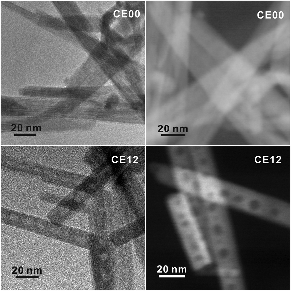 | ||
| Fig. 2 TEM (left) and HAADF-STEM images (right) of indicated nanostructures. | ||
The discernible lattice-fringe image of Fig. 3a and the clear diffraction spots of Fig. 3b indicate that a porous CdSe nanorod possesses a well-defined single crystalline structure. The interplanar distance of 0.35 nm observed from the lattice fringes of Fig. 3a accords with the theoretical spacing of 0.352 nm between the (002) planes of wurtzite CdSe (JCPDS no. 08-0459). The d-spacing of 0.34 nm calculated from the brightest diffraction spot in the FFT pattern of Fig. 3b also agrees reasonably with the spacing of the (002) planes, implying that the as-synthesized porous CdSe nanorod has a preferred [001] orientation.3,4 To verify whether the as-synthesized porous CdSe nanorod indeed has nanocavities, its line-scanned EDX elemental profiles have also been examined; although the bright region in the HAADF-STEM image of Fig. 3c has a flat elemental profile for both Cd and Se, the dark circular region in the HADDF-STEM image of Fig. 3d has a parabolic-shaped elemental profile, which is a common feature of hollow structures, for both Cd and Se.26,35 Interestingly, the atomic ratio of [Se]-to-[Cd] calculated from the integrated elemental profiles of Fig. 3c is 0.92 whereas the ratio calculated from Fig. 3d is 0.76. This indicates that while selenium vacancies are rich in a porous CdSe nanorod, they are three times richer in void regions than in filled regions. Considering this observation, we suggest that Se anions diffuse out faster than Cd cations during the hydrothermal process of CdSe·(en)0.5 nanorods and that the diffusion of Se anions is particularly rapid near crystal defects (see below).
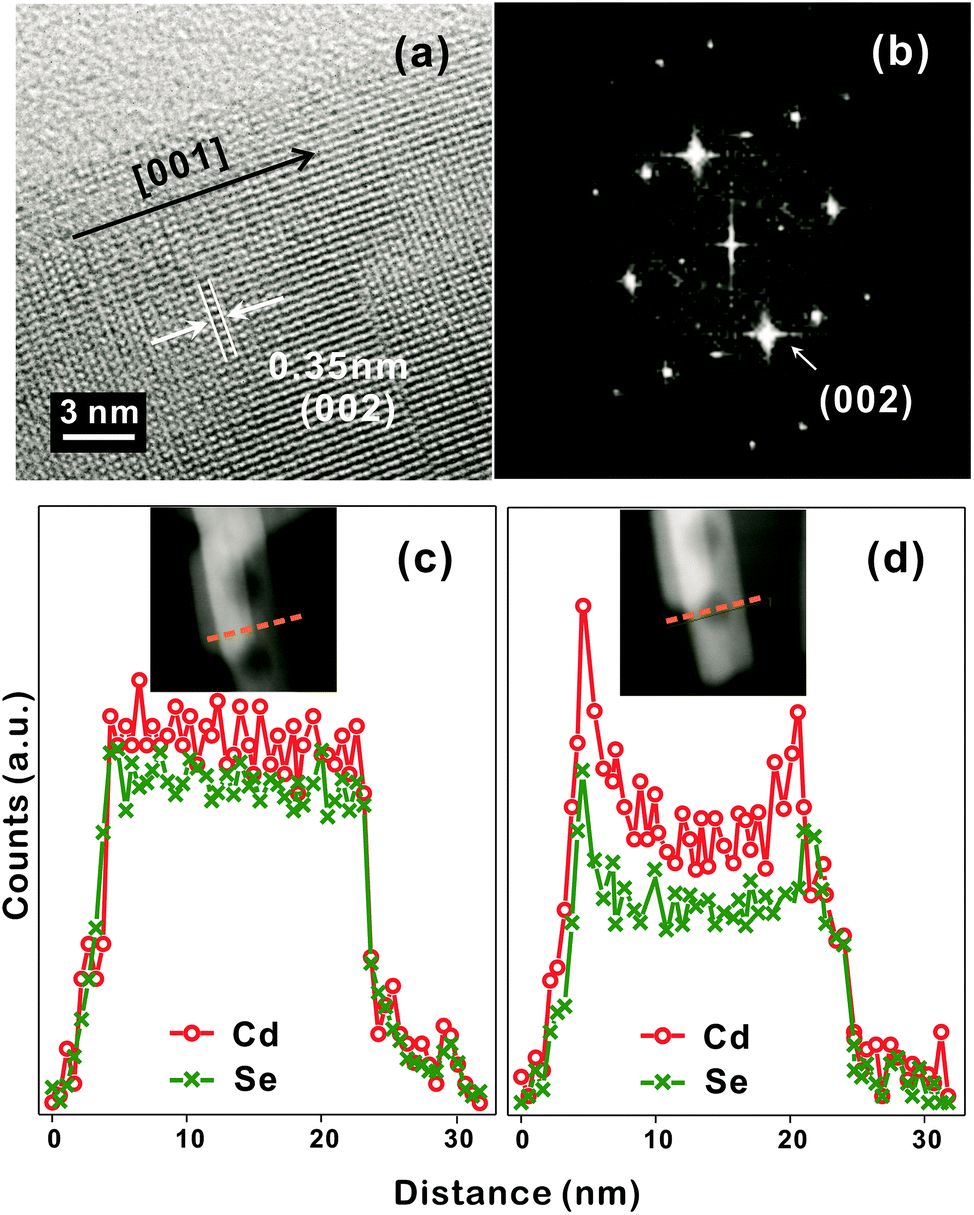 | ||
| Fig. 3 HRTEM image (a), FFT pattern (b), and STEM-EDX elemental profiles (c, d), scanned along the lines in the HAADF images of the insets, of a CE12 porous nanorod. | ||
 | ||
| Fig. 4 HRXRD patterns of indicated nanostructures. The standard diffraction pattern of CdSe (JCPDS no. 08-0459) is also shown at the bottom. | ||
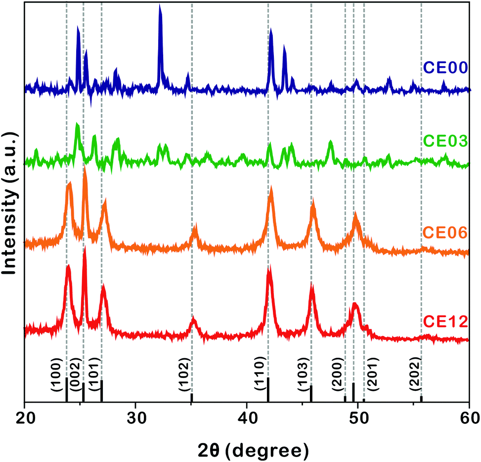
The HRXRD patterns of Fig. 4 show the structural evolution of CdSe·(en)0.5 nanorods with the increase of the hydrothermal-treatment time. The diffraction patterns of nanostructures prepared by the hydrothermal treatment of CdSe·(en)0.5 nanorods for 0 and 3 h can be correlated well with the reported pattern of the orthorhombic CdSe·(en)0.5.13,14 However, the diffraction patterns of CE06 and CE12 nanorods produced by the hydrothermal treatment of CdSe·(en)0.5 nanorods for 6 and 12 h, respectively, agree well with the standard pattern of the hexagonal wurtzite CdSe (JCPDS no. 08-0459). It means that the complete transformation of orthorhombic CdSe·(en)0.5 nanostructures into wurtzite CdSe nanostructures via hydrothermal treatment at 150 °C takes longer than 3 h. The characteristic diffraction peaks of CE06 and CE12 CdSe nanorods at a 2θ value of 25.2°, which arise from the (002) planes of the wurtzite CdSe, are particularly strong in comparison with diffraction peaks arising from any other planes. This indicates that our CE06 and CE12 CdSe nanorods have a preferred [001] orientation, as already described with the HRTEM image of Fig. 3a and the FFT pattern of Fig. 3b. Using the Scherrer equation17 and assuming that peak broadening arises entirely from size effects, we have calculated average crystallite sizes by using the peaks at a 2θ of ∼42°. The average crystallite sizes of CE00, CE03, CE06, and CE12 nanostructures have been calculated as 27.5, 24.5, 10.2, and 9.8 nm, respectively, indicating that the average crystallite size of CdSe·(en)0.5 nanorods decreases with hydrothermal treatment. In particular, during a hydrolysis time between 3 and 6 h, crystallite sizes reduce extensively. This also supports the fact that the transformation of orthorhombic CdSe·(en)0.5 nanorods into wurtzite CdSe nanorods takes place essentially during a hydrothermal treatment time between 3 and 6 h.
HRXRD profiles can provide significant information about the structural defects because internal stress, caused by misfit at grain boundaries, can change lattice parameters such as lattice constants and interplanar spacings.36,37 Thus, diffraction patterns from distorted crystallites are different in the location and broadening of a peak. In the case of internal tensile stress resulting from planar defects, HRXRD peaks are known to shift to a higher angle than the standard diffraction pattern.36Fig. 4 shows that the XRD peaks of CE06 and CE12 have small shifts to higher angles, indicating that there are structural defects in both CdSe nanostructures. It is noteworthy that the peak shifts of CE12 are smaller than those of CE06, suggesting that the internal stress of planar defects relaxes gradually during the late stage of hydrothermal treatment (see below).
The HRTEM images of Fig. 5 display the lattice evolution of CdSe·(en)0.5 nanorods with the increase of the hydrothermal-treatment time. In the early stage of a hydrothermal-treatment time of 3 h, highly defective regions, which are generally called as stacking faults, have been observed throughout the crystal lattice of a CE03 nanorod. These stacking faults are considered to arise from lattice mismatches between orthorhombic CdSe·(en)0.5 structures and hexagonal wurtzite CdSe structures. The observed stacking faults are parallel to each other and perpendicular to the growth direction of nanostructures. Thus, we suggest that the chemical transformation of orthorhombic CdSe·(en)0.5 nanorods into hexagonal wurtzite CdSe nanorods progresses in a layer-by-layer fashion.22 Stacking faults still remain in the crystal lattices of CE06 and CE09 nanostructures even after orthorhombic CdSe·(en)0.5 nanorods have been converted completely into hexagonal wurtzite CdSe nanorods. The remaining stacking faults such as the yellow lines of the CE09 HRTEM image of Fig. 5 function as twinning boundaries around which CdSe lattice segments align along the [001] direction in a zigzag manner.21,22,24,38 As the hydrothermal-treatment time increases, the observed number of plane defects decreases gradually, indicating that the internal stress of planar defects relaxes gradually during the late stage of the hydrothermal treatment. Owing to the self-healing process of planar defects, most of the stacking faults disappear eventually to produce highly crystalline CE12 CdSe nanorods.
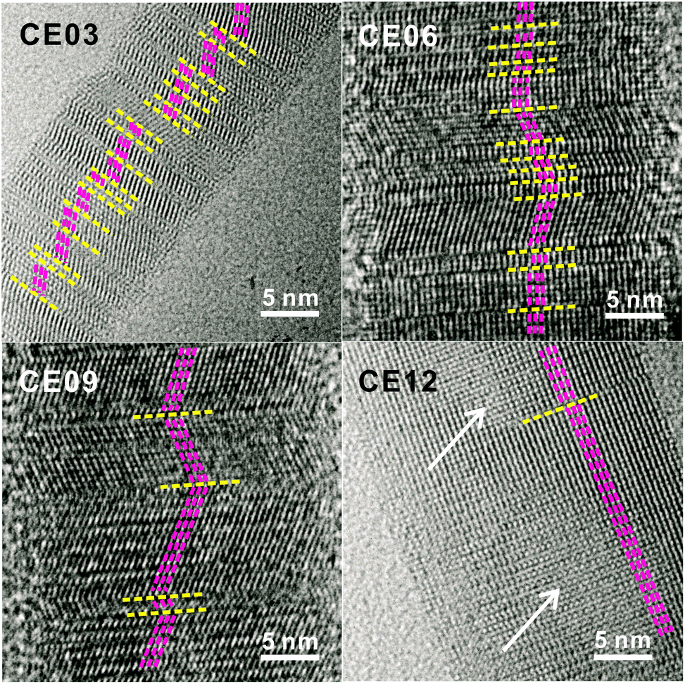 | ||
| Fig. 5 HRTEM images of indicated nanostructures. Yellow lines mark planar defects while pink lines and white arrows indicate lattice alignments and pore regions, respectively. | ||
When the crystal lattice is distorted, atomic diffusion can occur to release the excess elastic energy of the lattice.27,28,39 Twinning boundaries have been considered to become another fast diffusion path as a ‘pipe diffusion’ concept,40 and outward atomic diffusion can be particularly triggered near the twining plane sites during the self-healing process of planar defects. Due to the imbalance of atomic in-and-out diffusion, point defects can be severely generated near twinning boundaries, finally forming volume defects of voids in a CE12 CdSe nanorod. Therefore, we assert that the emergence of internal voids in a porous CdSe nanorod has been closely correlated with the disappearance of planar defects. However, the evidence of axial dislocation has not been observed in our nanorods, suggesting that our CdSe nanorods are unlikely to have grown via a screw-dislocation mechanism.23,27
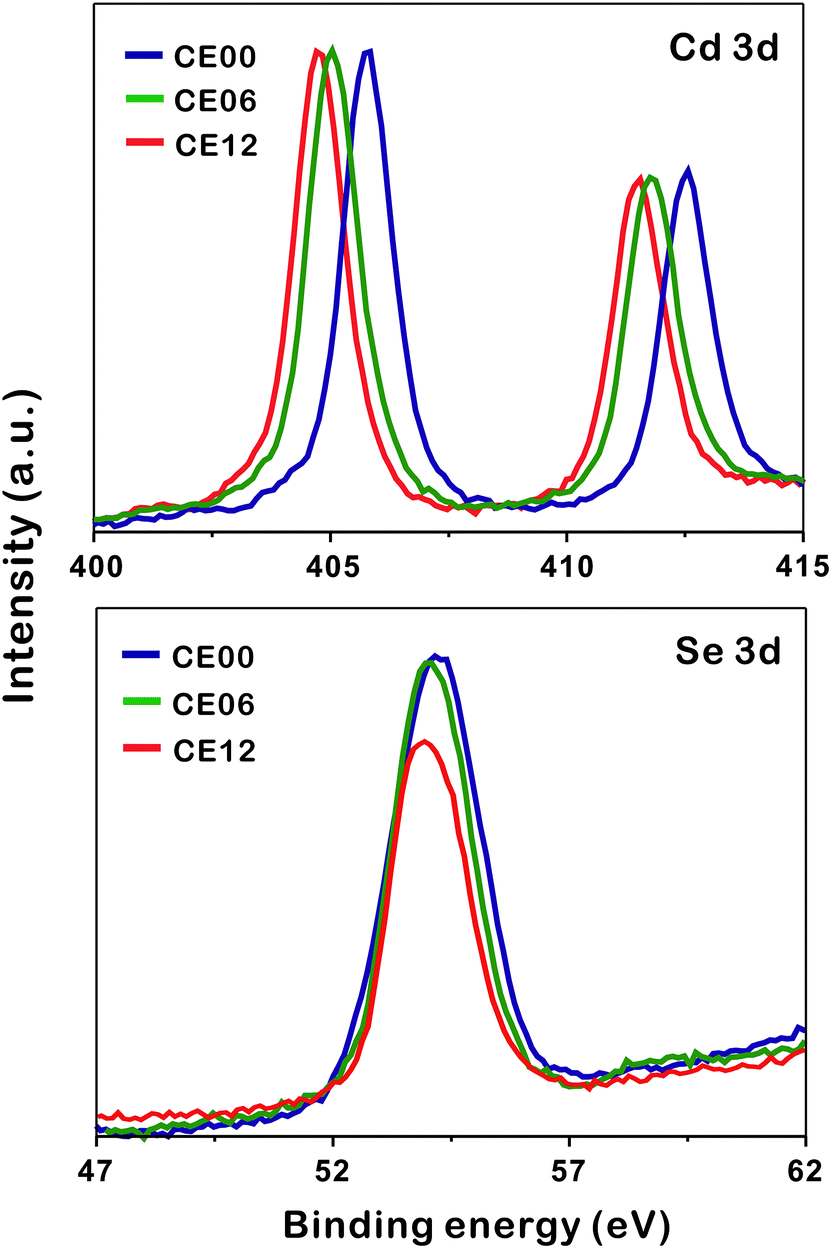
To understand the formation mechanisms of porous CdSe nanorods in detail, we have measured the XPS spectra of Cd 3d and Se 3d with the increase of the hydrothermal-treatment time (Fig. 6). The XPS peak positions of Cd 3d shift significantly to a low binding energy with the hydrolysis time whereas the XPS peak positions of Se 3d hardly shift (Table 1). As CE00 CdSe·(en)0.5 nanorods are transformed into CE06 CdSe nanorods, the binding energies of Cd 3d decrease significantly because the electronegativity of Se is smaller than that of N; the withdrawing of electron charges by neighboring atoms with high electronegativity increases the binding energies of electrons in an atom because the partial removal of electron charges reduces the electronic shielding. The further down shift of Cd 3d binding energies during a hydrolysis time between 6 and 12 h has been attributed to the increased presence of Se vacancies because it is generally known that adjacent anion vacancies reduce the binding energy of metal ions.41 Interestingly, Fig. 6 and Table 1 show that the atomic ratio of [Se]-to-[Cd] for porous CdSe nanorods is substantially smaller than one. This is also confirmed by the EDX spectra of Fig. S3.† As has already been described with the EDX elemental profiles of Fig. 3, selenium vacancies are rich particularly in CE12 porous CdSe nanorods, suggesting that Se anions diffuse out faster than Cd cations during the hydrothermal process of CdSe·(en)0.5 nanorods and that the diffusion of Se anions is rapid near crystal defects. We suggest that the generated selenium vacancy sites are filled with trapped electrons, oxide ions, or hydroxide ions to balance the overall charge of nanostructures. Summarizing the above presented results, we propose a dislocation-driven growth mechanism of porous CdSe nanorods from CdSe·(en)0.5 nanorods in Fig. 1.
 | ||
| Fig. 6 XPS spectra of indicated nanostructures. | ||
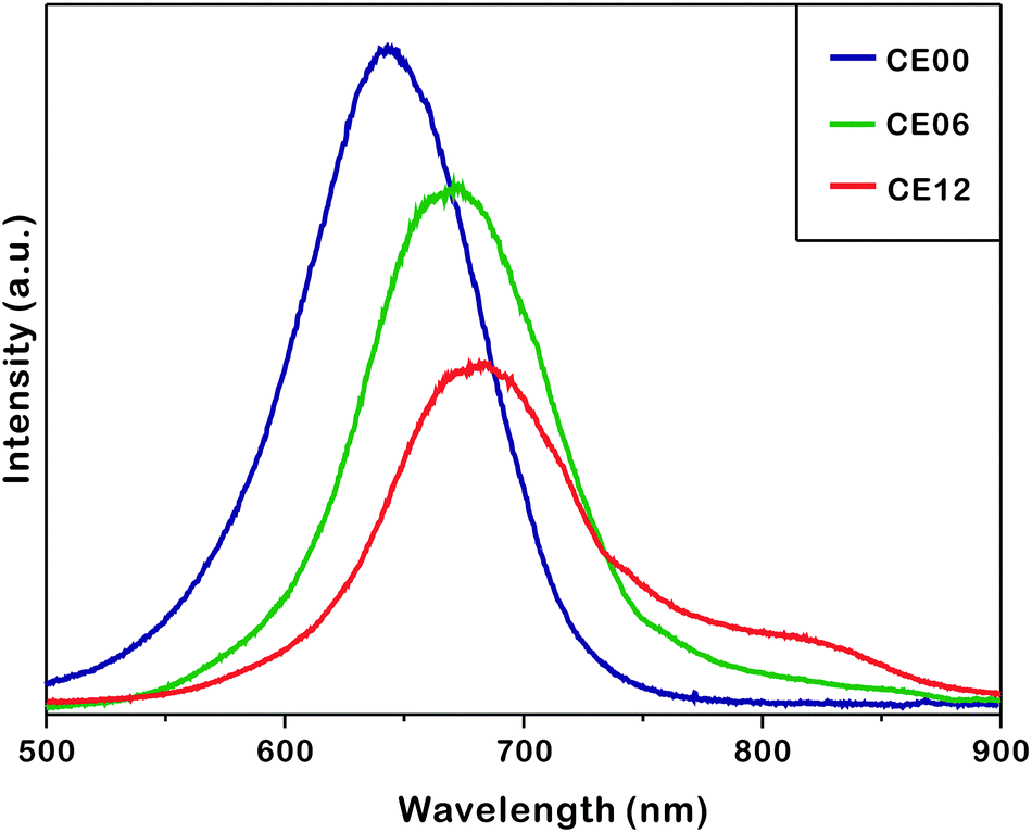
Fig. 7 shows that the photoluminescence of as-prepared nanostructures shifts to the red region and decreases in intensity as the hydrothermal-treatment time increases. The photoluminescence of CE06 CdSe nanorods shifts to the red region by 36 nm from that of CE00 CdSe·(en)0.5 nanorods at 635 nm as en molecules intercalated in CdSe layers are removed. The UV-visible extinction spectra of Fig. S5† show that in comparison with CE00 nanostructures, CE06 and CE12 nanostructures have an increased visible absorption with a discernible band around 630 nm, supporting that CdSe·(en)0.5 nanorods are successfully converted into CdSe nanostructures. Even after orthorhombic CdSe·(en)0.5 nanorods have been converted completely into hexagonal wurtzite CdSe nanorods, the photoluminescence of CE06 CdSe nanorods shifts further to the red region by 9 nm during a hydrothermal-treatment time between 6 and 12 h. Fig S4 and Table S1† indicate that the near-infrared shoulder band of photoluminescence at 784 nm, which has been attributed to arise from selenium vacancies and oxygen impurities,42 increases 4.8 times during a hydrothermal-treatment time between 6 and 12 h. This also supports the observation of Fig. 6 and Table 1 that selenium vacancies are particularly rich in CE12 porous CdSe nanorods. We consider that the development of near-infrared fluorophores is important due to potential applications such as in biology (imaging and tracking), telecommunications, and solar energy conversion (photovoltaics and photocatalysis).43,44 The continuous decrease of photoluminescence intensity with the increase of the hydrolysis time is attributed to increased surface states, which block the recombination of electrons in the conduction band with holes in the valence band, as Fig. 4 shows that the average crystallite sizes of nanorods decrease gradually with the increase of the hydrothermal treatment time.
 | ||
| Fig. 7 Photoluminescence spectra of indicated nanostructures suspended in ethanol with excitation at 355 nm. | ||
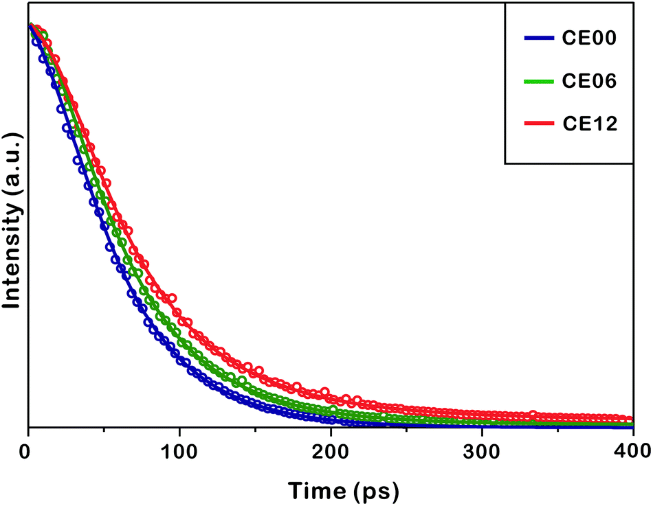
Fig. 8 and Table 2 indicate that the photoluminescence kinetic profiles of CE00 CdSe·(en)0.5 nanorods, CE06 CdSe nanorods, and CE12 porous CdSe nanorods look similar to one another with two decay components although their mean emission lifetime increases with the increase of the hydrothermal-treatment time. The fast decay component of 60 ps has been attributed to the intrinsic recombination of electrons in the conduction band whereas the slow decay component of 270 ps is considered to arise from the radiative recombination of charge carriers in surface states.45–47 Thus, the increase of the mean lifetime with the increase of the hydrothermal-treatment time is due to the fractional-amplitude increment of the slow-decay component. This also supports our suggestion made in Fig. 7 that surface states increase with the hydrothermal-treatment time of CdSe·(en)0.5 nanorods. The decay kinetic profile of the near-infrared shoulder band of photoluminescence at ∼790 nm, which arises mainly from selenium vacancies, has been found to be too slow to be observed with our picosecond kinetic spectrometer because radiative transition from the relaxed excited state (2s) to the ground state (1s) of F-centers (selenium vacancies with two trapped electrons) is not allowed by the spectroscopic selection rule of Laporte.17,48
 | ||
| Fig. 8 Photoluminescence kinetic profiles of indicated nanostructures suspended in ethanol at room temperature, and solid lines are best-fitted curves to extract kinetic constants. Photoluminescence was monitored at 670 ± 5 nm after excitation at 355 nm. | ||
In the review process of this manuscript, it has been found that our nanostructures have low PLQYs of 4.4 (CE00), 3.8 (CE06), and 3.2% (CE12) (Table S1†), in consideration of the fact that PLQYs of reported CdSe nanocrystals are usually 10–86%.49–52 In general, the relaxation dynamics of photoexcited charge carriers proceed through radiative decay and non-radiative decay; while radiative decay is determined by the intrinsic properties of the exciton that depends on the size, shape, and composition of a nanocrystal, non-radiative decay is primarily determined by the conditions of surface states on the nanostructures.34 Thus, the surface defects of the planar defects (stacking faults and twinning boundaries) or volume defects (voids) in our as-prepared CdSe nanostructures can facilitate charge carrier-quenching, and therefore the photoluminescence decay dynamics is dominated by non-radiative processes, resulting in low PLQYs. Thus, the fast photoluminescence decay times of our as-prepared CdSe nanostructures are strongly correlated with their low PLQYs.
Conclusions
Porous hexagonal wurtzite CdSe nanorods having an average length of 210 nm and a typical diameter of 20 nm with multiple voids ranging from 8 to 12 nm have been prepared facilely by treating orthorhombic CdSe·(en)0.5 nanorods hydrothermally. It has been found that various crystalline imperfections such as stacking faults and twinning planes appear during a hydrolysis time between 3 and 9 h and disappear subsequently during a hydrolysis time between 9 and 12 h to release lattice mismatch strains. Selenium vacancies are rich particularly in porous CdSe nanorods, suggesting that Se anions diffuse out faster than Cd cations during the hydrothermal process of CdSe·(en)0.5 nanorods and that the diffusion of Se anions is rapid near crystal defects. Due to the imbalance of in-and-out atomic diffusion, point defects of atomic vacancies are heavily generated in CdSe nanorods to produce volume defects of voids eventually. The photoluminescence of CdSe nanorods shifts to the red region and decreases in intensity with the increase of the hydrolysis time as surface states and selenium vacancies increase. The mean lifetime of photoluminescence increases with the increase of the hydrothermal-treatment time as the fractional amplitude of the slower-decay component, arising from the radiative recombination of charge carriers in surface states, increases.Acknowledgements
This work was supported by a research grant through the National Research Foundation (NRF) of Korea funded by the Korea government (2012-006345). We are also thankful to the SRC program of NRF (2007-0056331) and to Ms In-Sung Lee at the National Center for Inter-University Research Facilities for measuring HRTEM images.Notes and references
- Y. Liu, J. Goebl and Y. Yin, Chem. Soc. Rev., 2013, 42, 2610–2653 RSC.
- Y.-W. Jun, J.-S. Choi and J. Cheon, Angew. Chem., Int. Ed., 2006, 45, 3414–3439 CrossRef CAS PubMed.
- X. Peng, L. Manna, W. Yang, J. Wickham, E. Scher, A. Kadavanich and A. P. Alivisatos, Nature, 2000, 404, 59–61 CrossRef CAS PubMed.
- Z. A. Peng and X. Peng, J. Am. Chem. Soc., 2001, 123, 1389–1395 CrossRef CAS.
- J. Huang, M. V. Kovalenko and D. V. Talapin, J. Am. Chem. Soc., 2010, 132, 15866–15868 CrossRef CAS PubMed.
- Z. Li and X. Peng, J. Am. Chem. Soc., 2011, 133, 6578–6586 CrossRef CAS PubMed.
- H.-B. Kim, H. Kim, W. I. Lee and D.-J. Jang, J. Mater. Chem. A, 2015, 3, 9714–9721 CAS.
- J. T. Hu, L. S. Li, W. D. Yang, L. Manna, L. W. Wang and A. P. Alivisatos, Science, 2001, 292, 2060–2063 CrossRef CAS PubMed.
- H.-W. Liang, J.-W. Liu, H.-S. Qian and S.-H. Yu, Acc. Chem. Res., 2013, 46, 1450–1461 CrossRef CAS PubMed.
- X. Wang, Z. Li, J. Shi and Y. Yu, Chem. Rev., 2014, 114, 9346–9384 CrossRef CAS PubMed.
- S. Zhang, N. Tang, W. Jin, J. Duan, X. He, X. Rong, C. He, L. Zhang, X. Qin, L. Dai, Y. Chen, W. Ge and B. Shen, Nano Lett., 2015, 15, 1152–1157 CrossRef CAS PubMed.
- Z. Zhuang, Q. Peng and Y. Li, Chem. Soc. Rev., 2011, 40, 5492–5513 RSC.
- Z.-X. Deng, L. Li and Y. Li, Inorg. Chem., 2003, 42, 2331–2341 CrossRef CAS PubMed.
- X. Huang, J. Li, Y. Zhang and A. Mascarenhas, J. Am. Chem. Soc., 2003, 125, 7049–7055 CrossRef CAS PubMed.
- J. Yang, C. Xue, S.-H. Yu, J.-H. Zeng and Y.-T. Qian, Angew. Chem., Int. Ed., 2002, 41, 4697–4700 CrossRef CAS PubMed.
- J.-Y. Kim, M. R. Kim, S.-Y. Park and D.-J. Jang, CrystEngComm, 2010, 12, 1803–1808 RSC.
- Y. Kim, J.-Y. Kim and D.-J. Jang, J. Phys. Chem. C, 2012, 116, 10296–10302 CAS.
- Y. Kim and D.-J. Jang, CrystEngComm, 2014, 16, 6989–6995 RSC.
- J. Zhang, J. Yu, Y. Zhang, Q. Li and J. R. Gong, Nano Lett., 2011, 11, 4774–4779 CrossRef CAS PubMed.
- D. Hull and D. J. Bacon, Introduction to Dislocations, Elsevier, Oxford, 5th edn, 2011 Search PubMed.
- S. M. Hughes and A. P. Alivisatos, Nano Lett., 2013, 13, 106–110 CrossRef CAS PubMed.
- M. I. B. Utama, M. de la Mata, C. Magen, J. Arbiol and Q. Xiong, Adv. Funct. Mater., 2013, 23, 1636–1646 CrossRef CAS.
- F. Meng, M. Estruga, A. Forticaux, S. A. Morin, Q. Wu, Z. Hu and S. Jin, ACS Nano, 2013, 7, 11369–11378 CrossRef CAS PubMed.
- M. Liu, D. Jing, Z. Zhou and L. Guo, Nat. Commun., 2013, 4, 2278 Search PubMed.
- M. I. B. Utama, Q. Zhang, S. Jia, D. Li, J. Wang and Q. Xiong, ACS Nano, 2012, 6, 2281–2288 CrossRef CAS PubMed.
- M. Kumar, V. N. Singh, B. R. Mehta and J. P. Singh, J. Phys. Chem. C, 2012, 116, 5450–5455 CAS.
- D. Maestre, D. Häussler, A. Cremades, W. Jäger and J. Piqueras, J. Phys. Chem. C, 2011, 115, 18083–18087 CAS.
- W. Xu, Y. Zhang, G. Cheng, W. Jian, P. C. Millett, C. C. Koch, S. N. Mathaudhu and Y. Zhu, Nat. Commun., 2013, 4, 2288 Search PubMed.
- L. Zhao, L. Hu and X. Fang, Adv. Funct. Mater., 2012, 22, 1551–1566 CrossRef CAS.
- L. Li, H. Lu and K. Deng, J. Mater. Chem. A, 2013, 1, 2089–2093 CAS.
- C. Zhu, D. Du, A. Eychmüller and Y. Lin, Chem. Rev., 2015, 115, 8896–8943 CrossRef CAS PubMed.
- V. Valtchev and L. Tosheva, Chem. Rev., 2013, 113, 6734–6760 CrossRef CAS PubMed.
- W. Wang, M. Dahl and Y. Yin, Chem. Mater., 2013, 25, 1179–1189 CrossRef CAS.
- D. Choi, J.-Y. Pyo, Y. Kim and D.-J. Jang, J. Mater. Chem. C, 2015, 3, 3286–3293 RSC.
- Y. Kim, H.-B. Kim and D.-J. Jang, J. Mater. Chem. A, 2014, 2, 5791–5799 CAS.
- W. Y. Park, M. H. Park, J. H. Lee, J. H. Yoon, J. H. Han, J.-H. Choi and C. S. Hwang, Sci. Rep., 2012, 2, 939 Search PubMed.
- H. V. Swygenhoven, P. M. Derlet and A. G. Frøseth, Nat. Mater., 2004, 3, 399 CrossRef PubMed.
- H. Shi, B. Dong and W. Wang, Nanoscale, 2012, 4, 6389 RSC.
- M. de la Mata, C. Magén, P. Caroff and J. Arbiol, Nano Lett., 2014, 14, 6614–6620 CrossRef CAS PubMed.
- Y. Tang and M. Ouyang, Nat. Mater., 2007, 6, 754–759 CrossRef CAS PubMed.
- G. Wang, B. Huang, Z. Li, Z. Lou, Z. Wang, Y. Dai and M.-H. Whangbo, Sci. Rep., 2015, 5, 8544 CrossRef CAS PubMed.
- M. J. S. P. Brasil, P. Motisuke, F. Decker and J. R. Moro, J. Phys. C: Solid State Phys., 1988, 21, 3141–3150 CrossRef CAS.
- S. Kim, Y. T. Lim, E. G. Soltesz, A. M. De Grand, J. Lee, A. Nakayama, J. A. Parker, T. Mihaljevic, R. G. Laurence, D. M. Dor, L. H. Cohn, M. G. Bawendi and J. V. Frangioni, Nat. Biotechnol., 2004, 22, 93–97 CrossRef CAS PubMed.
- Y. J. Guo, C. E. Rowland, R. D. Schaller and J. Vela, ACS Nano, 2014, 8, 8334–8343 CrossRef CAS PubMed.
- Z.-J. Jiang and D. F. Kelley, J. Phys. Chem. C, 2010, 114, 17519–17528 CAS.
- M. R. Kim, J. H. Chung, M. Lee, S. Lee and D.-J. Jang, J. Colloid Interface Sci., 2010, 350, 5–9 CrossRef CAS PubMed.
- M. R. Kim, S.-Y. Park and D.-J. Jang, J. Phys. Chem. C, 2010, 114, 6452–6457 CAS.
- P. Rinke, A. Schleife, E. Kioupakis, A. Janotti, C. Rödl, F. Bechstedt, M. Scheffler and C. G. Van de Walle, Phys. Rev. Lett., 2012, 108, 126404 CrossRef PubMed.
- X. Wang, L. Qu, J. Zhang, X. Peng and M. Xiao, Nano Lett., 2003, 3, 1103–1106 CrossRef CAS.
- M. Jones, J. Nedeljkovic, R. J. Ellingson, A. J. Nozik and G. Rumbles, J. Phys. Chem. B, 2003, 107, 11346 CrossRef CAS.
- H. Y. Duan, Y. Jiang, Y. G. Zhang, D. P. Sun, C. Liu, J. Huang, X. Z. Lan, H. Y. Zhou, L. Chen and H. H. Zhong, Nanotechnology, 2013, 24, 285201 CrossRef PubMed.
- A. V. Antanovich, A. V. Prudnikau, D. Melnikau, Y. P. Rakovich, A. Chuvilin, U. Woggon, A. W. Achtsteine and M. V. Artemyev, Nanoscale, 2015, 7, 8084 RSC.
Footnote |
| † Electronic supplementary information (ESI) available: Supplementary figures (Fig. S1–S4) and tables (Table S1). See DOI: 10.1039/c5nr06125c |
| This journal is © The Royal Society of Chemistry 2016 |