
Opening the band gap of graphene through silicon doping for the improved performance of graphene/GaAs heterojunction solar cells†
S. J.
Zhang
ab,
S. S.
Lin
*ab,
X. Q.
Li
ab,
X. Y.
Liu
c,
H. A.
Wu
c,
W. L.
Xu
ab,
P.
Wang
ab,
Z. Q.
Wu
ab,
H. K.
Zhong
ab and
Z. J.
Xu
ab
aCollege of Microelectronics, Zhejiang University, Hangzhou, 310027, China
bCollege of Information Science and Electronic Engineering, Zhejiang University, Hangzhou, 310027, China. E-mail: shishenglin@zju.edu.cn
cDepartment of Modern Mechanics, Chinese Academy of Sciences Key Laboratory of Mechanical Behavior and Design of Materials, University of Science and Technology of China, Hefei, 230000, China
First published on 26th November 2015
Abstract
Graphene has attracted increasing interest due to its remarkable properties. However, the zero band gap of monolayered graphene limits it's further electronic and optoelectronic applications. Herein, we have synthesized monolayered silicon-doped graphene (SiG) with large surface area using a chemical vapor deposition method. Raman and X-ray photoelectron spectroscopy measurements demonstrate that the silicon atoms are doped into graphene lattice at a doping level of 2.7–4.5 at%. Electrical measurements based on a field effect transistor indicate that the band gap of graphene has been opened via silicon doping without a clear degradation in carrier mobility, and the work function of SiG, deduced from ultraviolet photoelectron spectroscopy, was 0.13–0.25 eV larger than that of graphene. Moreover, when compared with the graphene/GaAs heterostructure, SiG/GaAs exhibits an enhanced performance. The performance of 3.4% silicon doped SiG/GaAs solar cell has been improved by 33.7% on average, which was attributed to the increased barrier height and improved interface quality. Our results suggest that silicon doping can effectively engineer the band gap of monolayered graphene and SiG has great potential in optoelectronic device applications.
Graphene, a two-dimensional (2D) material discovered in 2004
![[thin space (1/6-em)]](https://www.rsc.org/images/entities/char_2009.gif) 1 with many remarkable properties, such as anomalous quantum hall effect, high electron mobility at room temperature, excellent thermal conductivity, and 97.7% transmittance of visible light, has attracted wide attention to various applications in electronic and optoelectronic areas.2–6 Although enormous efforts have been devoted to the research and potential applications of graphene, its intrinsic property of a zero band gap casts great obstacles on its further applications. Therefore, many approaches have been carried out to overcome this disadvantage.7–11 Among such methods, doping is considered as one of the most feasible ways to open the band gap of graphene and tailor its electrical properties, because doping can break the symmetry of the graphene lattice. For instance, hydrogenated graphene has been used to open the band gap of graphene,12 which can reach as large as 5.4 eV via controlling the coverage and configuration of the hydrogen atoms on the surface of graphene.13 Unfortunately, the distribution and the number of hydrogen atoms absorbed on graphene have a significant influence on the stability of the hydrogenated graphene, leading to unsustainable controlled electrical properties.14 When compared with hydrogenation, substitutional doping will break the symmetry of graphene by replacing the hexagonal carbon atoms with dopant atoms, such as N, B and Bi,15–18 which can tailor the electrical properties to be more stable than theoretically predicted. In practice, N-doped graphene can be controllably realized, using processes such as annealing in an NH3 atmosphere and synthesis using pyridine, which can open the band gap of graphene and shift the Fermi level into the conduction band.19–22 In addition, using a chemical vapor deposition (CVD) synthesis or thermal exfoliation of graphite in an atmosphere/solution comprising boron atoms, B-doped graphene can be achieved.23–25 In particular, the band gap of graphene can reach about 0.7 eV via nitrogen and boron combined doping,26,27 but the maldistribution of small BN domains impedes the application of this material in nanoscale optoelectronic devices.28 Unlike nitrogen and boron, silicon is an element in the same main group of carbon, so silicon doping is expected to open the band gap of graphene without affecting the carrier concentration. However, silicon doped graphene (SiG) has not been well-explored both theoretically and experimentally. To date, periodic density functional theory calculations of SiG show that the band gap will increase as the number of dopant silicon atoms increases and will exceed 2 eV when the ratio reaches 0.5.29 Moreover, SiG has potential to be applied in gas sensors as it is more reactive when absorbing small amounts of gas molecules such as CO, NO2, rhodamine B (RhB) and methylene blue (MB).30–33 When compared with the occasional discovery of SiG during the CVD growth of graphene,31 Lv et al. have controllably produced SiG through the reaction of methoxytrimethylsilane (MTMS, C4H12OSi) and hexane.33 However, the reported electrical measurements and practical applications of this material in the optoelectronic field are limited. In this study, SiG with a Si doping concentration of 2.7–4.5 at% has been obtained, which is used to form SiG/GaAs heterostructured solar cells. The best PCE of SiG/GaAs solar cell is 33.7% higher than that of graphene/GaAs devices on average with a Si doping concentration of 3.4 at%, as a result of opening the band gap of graphene up to 0.28 eV.
1 with many remarkable properties, such as anomalous quantum hall effect, high electron mobility at room temperature, excellent thermal conductivity, and 97.7% transmittance of visible light, has attracted wide attention to various applications in electronic and optoelectronic areas.2–6 Although enormous efforts have been devoted to the research and potential applications of graphene, its intrinsic property of a zero band gap casts great obstacles on its further applications. Therefore, many approaches have been carried out to overcome this disadvantage.7–11 Among such methods, doping is considered as one of the most feasible ways to open the band gap of graphene and tailor its electrical properties, because doping can break the symmetry of the graphene lattice. For instance, hydrogenated graphene has been used to open the band gap of graphene,12 which can reach as large as 5.4 eV via controlling the coverage and configuration of the hydrogen atoms on the surface of graphene.13 Unfortunately, the distribution and the number of hydrogen atoms absorbed on graphene have a significant influence on the stability of the hydrogenated graphene, leading to unsustainable controlled electrical properties.14 When compared with hydrogenation, substitutional doping will break the symmetry of graphene by replacing the hexagonal carbon atoms with dopant atoms, such as N, B and Bi,15–18 which can tailor the electrical properties to be more stable than theoretically predicted. In practice, N-doped graphene can be controllably realized, using processes such as annealing in an NH3 atmosphere and synthesis using pyridine, which can open the band gap of graphene and shift the Fermi level into the conduction band.19–22 In addition, using a chemical vapor deposition (CVD) synthesis or thermal exfoliation of graphite in an atmosphere/solution comprising boron atoms, B-doped graphene can be achieved.23–25 In particular, the band gap of graphene can reach about 0.7 eV via nitrogen and boron combined doping,26,27 but the maldistribution of small BN domains impedes the application of this material in nanoscale optoelectronic devices.28 Unlike nitrogen and boron, silicon is an element in the same main group of carbon, so silicon doping is expected to open the band gap of graphene without affecting the carrier concentration. However, silicon doped graphene (SiG) has not been well-explored both theoretically and experimentally. To date, periodic density functional theory calculations of SiG show that the band gap will increase as the number of dopant silicon atoms increases and will exceed 2 eV when the ratio reaches 0.5.29 Moreover, SiG has potential to be applied in gas sensors as it is more reactive when absorbing small amounts of gas molecules such as CO, NO2, rhodamine B (RhB) and methylene blue (MB).30–33 When compared with the occasional discovery of SiG during the CVD growth of graphene,31 Lv et al. have controllably produced SiG through the reaction of methoxytrimethylsilane (MTMS, C4H12OSi) and hexane.33 However, the reported electrical measurements and practical applications of this material in the optoelectronic field are limited. In this study, SiG with a Si doping concentration of 2.7–4.5 at% has been obtained, which is used to form SiG/GaAs heterostructured solar cells. The best PCE of SiG/GaAs solar cell is 33.7% higher than that of graphene/GaAs devices on average with a Si doping concentration of 3.4 at%, as a result of opening the band gap of graphene up to 0.28 eV.
The optical image of SiG transferred to a SiO2/Si wafer is shown in Fig. 1a, whereas the inset displays the schematic of SiG. From this image, we can observe that the transferred SiG was homogeneous on a centimeter scale. As shown in the Raman spectra of SiG and graphene film displayed in Fig. 1b, there are three main peaks assigned in the spectra, i.e. D peak (1354 cm−1), G peak (1593 cm−1) and 2D peak (2793 cm−1). In the Raman spectrum of graphene, the intensity ratio of the 2D peak to G peak (I2D/IG = 2.9) can be regarded as a typical feature of monolayered graphene. Moreover, the weak D peak indicates the high quality of the as-synthesized graphene. Due to the absorption of water and oxygen, the position of the G peak shifts to 1593 cm−1, indicating that graphene was p-type doped.34 When compared with the spectrum of graphene, no significant shifts of the G peak and 2D peak can be observed in SiG. However, a strong D peak appeared in the spectrum of SiG. This phenomenon was caused by the insertion of silicon atoms, which breaks the symmetry of the graphene lattice (the inset of Fig. 1a).14 Moreover, the strengthening in intensity of the D peak decreases the intensity ratio of the 2D peak to G peak. Fig. 1c and d illustrate the X-ray photoelectron spectroscopy (XPS) spectra of the silicon doped and pristine graphene films. The SiG and graphene membranes were transferred onto the Ge substrate to avoid the influence of silicon in the Si/SiO2 substrate. As shown in Fig. 1c, both SiG and graphene have a significant signal for the sp2 hybridized C–C bonds at around 284.4 eV, indicating the component of graphitic carbon.35 Two additional signals, one peak assigned to 101.2 eV and another located at 103.3 eV, are observed during the Si 2p scanning of the SiG sheet (Fig. 1d). The difference between the C 1s and Si 2p binding energies of graphitic SiC was 183–184 eV, which was larger than that found for bulk SiC. This result is in accordance with our previous XPS analysis on 2D SiC.36 To the best of our knowledge on 2D SiC, the XPS peak located at 100–101.2 eV can be ascribed to the Si–C3 (sp3) configuration.36,37 It was found in the STEM measurements that Si can adopt Si–C3 or Si–C4 configurations,37 thus the detailed configuration of Si in the honeycomb C lattice plane for the Si 2p peaks at 103.2 eV remains unknown. However, one conclusion can be made that silicon with an sp3 configuration has been definitely doped into the 2D graphene lattice. We define the doping level of silicon by the quantitative atomic ratio of Si (100 eV–101.2 eV band) to C (284.4 eV band). In the following sections, unless specified, the silicon doped graphene mentioned here means a doping level of 3.4 at%. We have also synthesized SiG with different Si concentrations, which were measured from 2.7 at% to 4.5 at% by changing the flux ratio of SiH4 to CH4. The characterization results can be found in Fig S1.† The main purpose of our study was to investigate the band gap opening of graphene by silicon doping compared with intrinsic graphene and its potential applications in graphene/semiconductor optoelectronic devices.
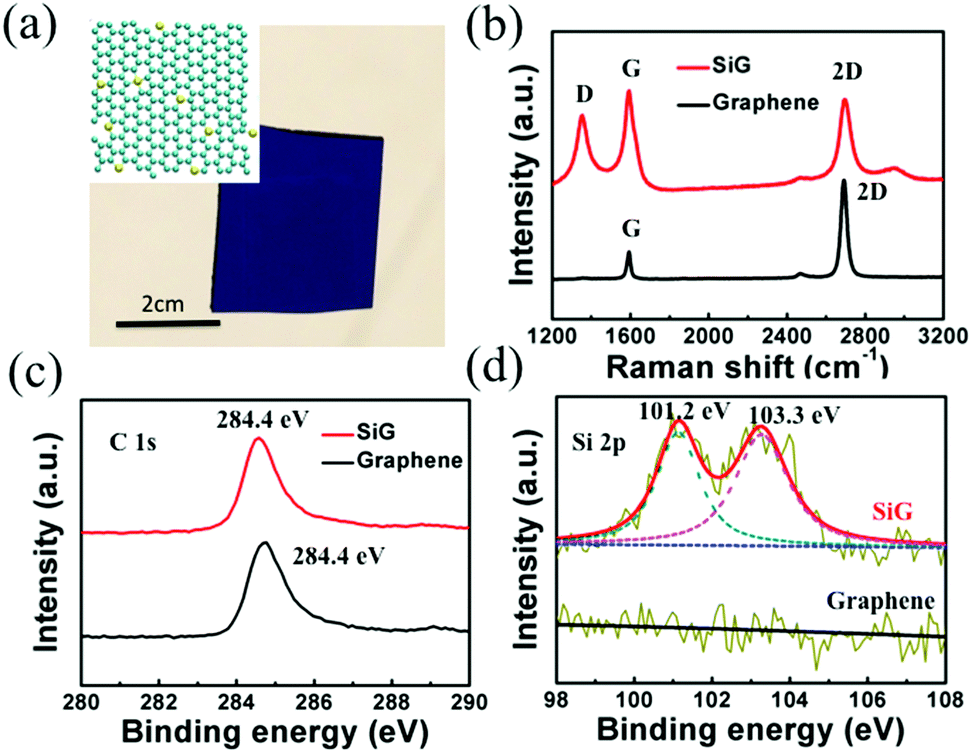 | ||
| Fig. 1 (a) The optical image of SiG transferred to a SiO2/Si wafer. The inset is the schematic of SiG, wherein several carbon atoms (blue balls) in the lattice are replaced by silicon atoms (yellow balls). (b) Raman spectra of SiG and graphene on a SiO2/Si substrate. (c) and (d) XPS spectra of the SiG and graphene sheets. As shown in (c), there was no dramatic difference in the peak of graphite-like sp2 C between SiG and graphene. From (d), the clear peaks of Si 2p at 101.1 eV and 103.3 eV can be detected in SiG, providing reliable evidence for silicon doping. | ||
Fig. 2a shows the low magnification transmission electron microscopy (TEM) image of the SiG membrane. The electron diffraction image inserted in the left region of Fig. 2a shows the honeycomb structure of SiG on the nanoscale. The TEM image taken from the edge of the SiG membrane marked with a red rectangle illustrated in Fig. 2b clearly shows the SiG film is monolayered. The thickness of SiG transferred to the SiO2/Si (90 nm/500 μm) substrate was measured using atomic force microscopy (AFM). As shown in Fig. 2c, the membrane was almost smooth in the whole area except the edge region with some folders and cracks caused during the transfer process. Moreover, the height of the SiG (0.37 nm) was similar to that of monolayered graphene (0.35 nm).38
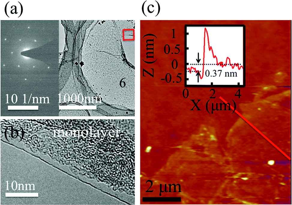 | ||
| Fig. 2 (a) A low magnification TEM image of the suspended SiG membrane. The electron diffraction pattern inserted in the left of (a) shows that the structure of SiG was honeycomb. (b) HRTEM images of the SiG sheet on the TEM grid in the area identified by the red rectangle. (c) AFM image of the SiG film. The inset demonstrates that the height of the SiG along the red line was around 0.37 nm. | ||
Ultraviolet photoelectron spectroscopy (UPS) of the SiG and graphene are shown in Fig. 3a. The kinetic energies are drawn after correction with an applied bias of −9.8 V and the analyser work function, thus the work function of graphene can be directly obtained from the intersection between the base line of the spectrum and the tangent of the sample secondary electron cut off. As shown in Fig. 3a, the work function of SiG was 4.63 eV, which is 0.13 eV larger than that found for graphene (4.5 eV). The work functions of the other two SiG sheets are shown in Fig. S2,† wherein the work function of SiG with a Si doping concentration of 4.5 at% was 0.25 eV higher than graphene. Moreover, a back-gated field effect transistor (FET) was fabricated using both SiG and graphene for electrical measurements. Fig. 3b shows the structure of the FET, which includes the Au electrodes, SiG/graphene, SiO2 and highly doped silicon. Graphene and SiG, bridging the source and drain electrodes, act as the conducting channel, which was 2 mm wide by 1 mm long. The transport characteristics of the current between the drain and source (IDS) vs. back gate voltage (VG) are illustrated in Fig. 3c. In the measurement, the bias voltage of 1 V was fixed. According to the IDSvs. VG curve, the voltage at the Dirac point shifts to the positive direction, originating from the absorption of oxygen and water molecules, which cause graphene to be p-type doped.34 Moreover, the carrier mobility (μ) can be deduced using eqn (1)
 | (1) |
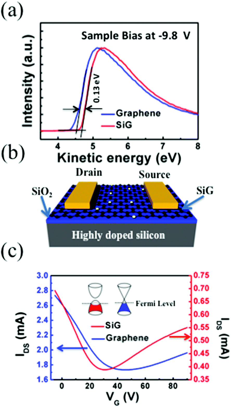 | ||
| Fig. 3 (a) UPS of the SiG and graphene film. (b) The schematic of the FETs based on SiG. (c) Transfer characteristics of SiG and graphene. | ||
Because the silicon atoms have formed a covalent bond with the carbon atoms in the graphene lattice and the symmetry of the graphene lattice was broken, opening of the band gap of graphene was expected.29 To evaluate the band gap opened by silicon doping, first-principle calculations were performed to investigate the electronic structure of the SiG. As shown in Fig. 4a, the initial atomic configuration was optimized before the band energy calculation and the percentage of silicon atoms was 3.1% in the SiG monolayer. The band structure illustrated in Fig. 4b shows a band gap at K point with a value of 0.28 eV.
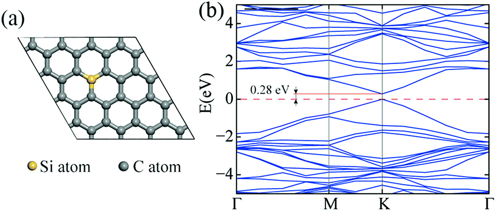 | ||
| Fig. 4 (a) The atomic configuration of SiG in which the percentage of silicon atoms was 3.1%. (b) The band structure of SiG. | ||
To further explore the potential application of SiG, we used this material to fabricate a SiG/GaAs solar cell. Fig. 5a shows the schematic of the solar cell, which comprised a silver electrode, SiG membrane, SiNx, GaAs and Au back electrode. SiG was transferred to the n-GaAs using a wet transferring process. Due to the work function difference between SiG and n-GaAs, some of the electrons in GaAs move to SiG, forming a heterojunction with a depletion region in the GaAs. When the photons are absorbed in the GaAs, electron–hole pairs are generated and separated by the build-in barrier located in the depletion region, leading to the electrons and holes to be collected by the GaAs and SiG, respectively, as shown in Fig. 5b. Fig. 5c displays the current density–voltage (J–V) curves for the solar cell with SiG and graphene under AM1.5G illumination at 100 mW cm−2. When comparing the performance of the SiG/GaAs solar cell with that of a graphene/GaAs solar cell, the short-circuit current density (Jsc), open-circuit voltage (Voc) and fill factor (FF) increase from 11.8 mA cm−2 to 13.6 mA cm−2, 0.59 V to 0.65 V and 50% to 51%, respectively, which boosts the power conversion efficiency (PCE) from 3.5% to 4.5%. The PCE distribution of each of the 13 samples of the SiG/GaAs and graphene/GaAs solar cells is illustrated in Fig. 5d, wherein it can be observed that the PCE of the SiG/GaAs solar cells has been generally improved. The average PCE of the SiG/GaAs solar cells was 3.69%, whereas that found for the graphene/GaAs solar cells was 2.76%. J–V curves for another four specimens of the SiG/GaAs and graphene/GaAs solar cells whose PCE are close to their average value are shown in Fig. S3,† whereas the statistics of the PCE of SiG/GaAs solar cells with different silicon concentrations are displayed in Fig. S4.† The external quantum efficiency (EQE) of the SiG/GaAs and graphene/GaAs solar cells are presented in Fig. 5e. In our EQE system, the line shape incident light spot was equipped with a size of 5 mm × 0.3 mm. During the measurements, the incident light was illuminated on the central region of the solar cell devices. The heterogeneity of the photo-to-electricity performance across the whole active region may lead to the measured EQE deviating from the real performance. Thus, the average EQE curve measured from each of the four graphene/GaAs and SiG/GaAs devices are presented here. The EQE spectra of each of the 4 SiG/GaAs and graphene/GaAs solar cell devices are shown in Fig. S5 and S6.† There is a significant improvement in the EQE for the SiG/GaAs solar cell within the wavelength range of 300–670 nm. The EQE in the short wavelength range was mainly influenced by the recombination at the front surface region, bulk properties and rear surface quality affect the EQE in the long wavelength range.41,42 As the difference of recombination in the front surface region was dominated by interfacial states, the presence of the EQE improvement over the short wavelength range in the SiG/GaAs solar cell indicates that the device has a better interfacial quality than that of the intrinsic graphene/GaAs heterostructure.
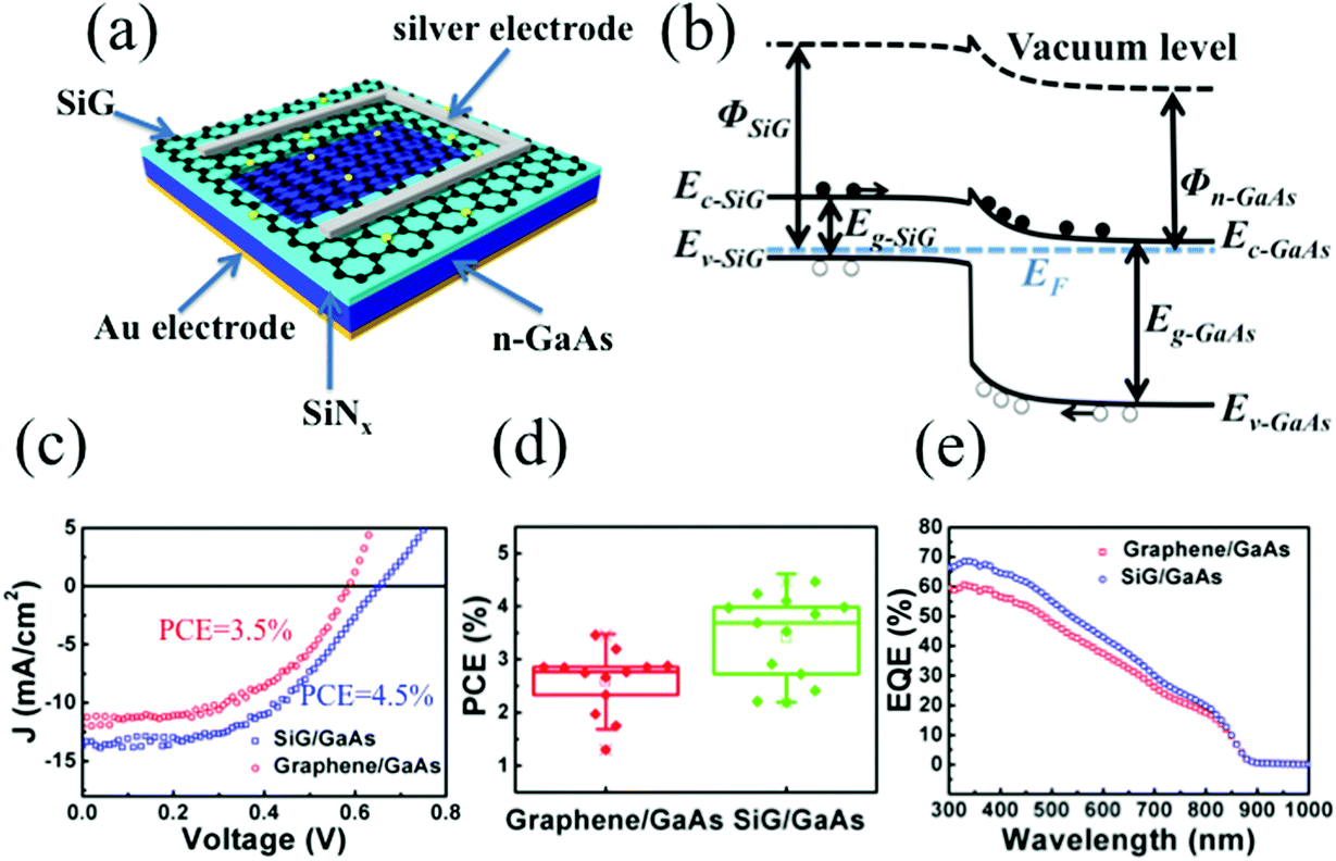 | ||
| Fig. 5 (a) Schematic of the SiG/GaAs solar cell. (b) The band diagram at the graphene/GaAs interface. (c) J–V curves for the SiG/GaAs solar cell and graphene/GaAs solar cell. (d) PCE distribution of the SiG and graphene/GaAs solar cell samples. (e) EQE of the SiG and graphene/GaAs solar cell. | ||
The physical parameters of the devices were further investigated. The barrier height (ΦBH) at the graphene/GaAs interface was determined by the difference in the work function of graphene (Φgr) and the electron affinity of GaAs (χGaAs), which was expressed as ΦBH = Φgr − χGaAs. With an increase in Φgr, ΦBH becomes larger. According to the UPS shown in Fig. 3a, the work function of SiG was 0.13 eV larger than that found for graphene, contributing to augment ΦBH, thus leading to an improvement in Voc.
Moreover, the dark J–V curves for the SiG/GaAs and graphene/GaAs (see Fig. S6†) heterostructures can be described using eqn (2)43,44
 | (2) |
 | (3) |
The Js of the graphene/GaAs junction deduced from eqn (2) was 2.66 × 10⁻⁴ mA cm−2 and that found for SiG/GaAs was 1.98 × 10⁻⁵ mA cm−2. The further deduced barrier height of graphene/GaAs was 0.74 eV, whereas that found for SiG/GaAs was 0.82 eV. This increased ΦBH contributes to the improvement of the Voc. In particular, the increased ΦBH was smaller than the ideal value (the difference between the work function of SiG and graphene measured by UPS), resulting from the charge transfer between graphene (or SiG) and GaAs, and the interfacial states that affect the value of ΦBH.48 The similar results by analysing another four SiG and graphene/GaAs solar cell devices (Fig. S3†) are shown in Table S1.†
Conclusions
In summary, monolayered SiG with a large surface area has been synthesized using CH4 and SiH4via a CVD method. The strong D Raman band and the clear peak of Si 2p in XPS demonstrated that the silicon atoms have been doped into the graphene lattice. Moreover, according to the electrical properties measured for SiG, we can come to a conclusion that the band gap of graphene was opened by silicon doping and the work function of SiG was 0.13–0.25 eV larger than that of pristine graphene. More importantly, when compared with the performance of the graphene/GaAs solar cell, the short circuit current and the open circuit voltage of the SiG/GaAs solar cells display a significant improvement, leading to a 33.7% enhancement of the PCE on average, which results from the increased work function of the SiG and the better interface between SiG and GaAs. This improvement in the SiG/GaAs solar cell indicates the potential applications of SiG in optoelectronic devices and our results will cast a new direction for further research of SiG.Experimental section
Synthesis and transfer of SiG
Large area SiG synthesis was accomplished via a CVD process; copper foils (99.8% purity, 25 μm thick, Alfa Aesar) were used as substrates for growth. During the growth process, the reactor was heated to 1015 °C under an Ar and H2 atmosphere, and the copper foils were annealed at this temperature for 30 min. Then, a mixed flow of SiH4 and CH4 was entered into the furnace to synthesize the SiG. Finally, the reactor was quickly cooled down to room temperature. The temperature profile is illustrated in Fig. S8.† During the reacting process, different flux ratios of SiH4 to CH4 (0.6 sccm:50 sccm, 1 sccm:50 sccm and 1.5 sccm:50 sccm) result in the synthesis of SiG with different Si doping levels (2.7 at%, 3.4 at% and 4.5 at%, respectively). However, currently continuous SiG cannot be fabricated with higher SiH4 to CH4 flux ratios. The SiG film was transferred to a SiO2/Si (300 nm/500 μm), germanium (Ge) or CaAs substrate using the following procedure: SiG on copper foil was coated with polymethyl methacrylate (PMMA) (4000 rpm min−1) and baked at 120 °C for 2 min. Subsequently, the copper was etched away using a Cu2SO4/HCl/H2O (16 mg/50 mL/50 mL) solution. Then, the SiG film with PMMA was transferred to the target substrate after cleaning in deionized water. Finally, the PMMA was removed using acetone.
Characterization of the SiG
Raman spectra of the SiG and pristine graphene membrane were obtained using a Renishaw micro-Raman spectrometer at an excitation wavelength of 532 nm with 50× objective. The UPS measurements of SiG and pristine graphene were directly carried out on graphene above copper (the He I Source was 21.2 eV), whereas the XPS was carried out on SiG and graphene transferred onto a Ge substrate (Escalab 250Xi). The suspended SiG membrane was transferred to the carbon TEM grid for morphology measurement using TEM (Tecnai F-30 operating at 300 kV), whereas the thickness of SiG was investigated by AFM (Veeco MultiMode).Fabrication and characterization of the effect field transistor (FET)
After cleaning the SiO2/Si (300 nm/500 μm) substrates in acetone (5 min) and isopropanol (5 min), the silicon doped and pristine graphene were transferred to the surface of SiO2/Si substrates. Then, the In–Ga alloy was pasted onto the surface of silicon to be used as the back electrode, whereas the Cr/Au (5 nm/60 nm) was thermally evaporated on the surface of SiG and pristine graphene for the source and drain electrodes, respectively. The transfer characteristics were measured using an Agilent B1500A system.Fabrication and characterization of the solar cells
The GaAs employed for solar cell fabrication was a single side polished monocrystalline n-type doped wafer with a doping concentration of around 1018 cm−3 and its thickness was 350 μm. Cr/Au (5 nm/60 nm) was thermally deposited on GaAs for the back Ohmic contact electrode, 80 nm SiNx was deposited on the GaAs via plasma enhanced CVD for a dielectric layer with the opened window defining the active area of the solar cell. Then, the opened window was cleaned using a HCl/H2O (1:3) solution and the SiG or graphene was transferred to the GaAs surface. Finally, the silver electrode was thermally deposited on the SiG or graphene surface above the SiNx dielectric layer. The finished SiG/GaAs and graphene/GaAs solar cells were tested with a solar simulator under AM1.5G illumination at 100 mW cm−2. The current–voltage data was recorded using a Keithley 4200 system. The EQE of the solar cells was measured using a PV measurements QEXL system.
Simulation of the band gap of SiG
First-principle calculations were performed using a plane wave open source code QUANTUM-ESPRESSO49 with the PBE exchange–correlation, Vanderbilt ultrasoft pseudopotentials, and a kinetic energy cutoff energy of 50 Ry.50 Visualization was performed using VESTA.51Notes and references
- K. S. Novoselov, A. K. Geim, S. V. Morozov, D. Jiang, Y. Zhang, S. V. Dubonos, I. V. Grigorieva and A. A. Firsov, Science, 2004, 306, 666–669 CrossRef CAS PubMed.
- K. S. Novoselov, Z. Jiang, Y. Zhang, S. V. Morozov, H. L. Stormer, U. Zeitler, J. C. Maan, G. S. Boebinger, P. Kim and A. K. Geim, Science, 2007, 315, 1379 CrossRef CAS PubMed.
- A. K. Geim, Science, 2009, 324, 1530–1534 CrossRef CAS PubMed.
- A. A. Balandin, S. Ghosh, W. Z. Bao, I. Calizo, D. Teweldebrhan, F. Miao and C. N. Lau, Nano Lett., 2008, 8, 902–907 CrossRef CAS PubMed.
- R. R. Nair, P. Blake, A. N. Grigorenko, K. S. Novoselov, T. J. Booth, T. Stauber, N. M. R. Peres and A. K. Geim, Science, 2008, 320, 1308–1308 CrossRef CAS PubMed.
- B. Zhu, Z. Q. Niu, H. Wang, W. R. Leow, H. Wang, Y. G. Li, L. Y. Zheng, J. Wei, F. W. Huo and X. D. Chen, Small, 2014, 10, 3625–2631 CrossRef CAS PubMed.
- A. Aparecido-Ferreira, H. Miyazaki, S. L. Li, K. Komatsu, S. Nakaharaic and K. Tsukagoshi, Nanoscale, 2012, 4, 7842–7846 RSC.
- A. Nourbakhsh, M. Cantoro, T. Vosch, G. Pourtois, F. Clemente, M. H. van der Veen, J. Hofkens, M. M. Heyns, S. De Gendt and B. F. Sels, Nanotechnology, 2010, 21, 435203 CrossRef PubMed.
- L. Y. Zhao, R. He, K. T. Rim, T. Schiros, K. S. Kim, H. Zhou, C. Gutierrez, S. P. Chockalingam, C. J. Arguello, L. Palova, D. Nordlund, M. S. Hybertsen, D. R. Reichman, T. F. Heinz, P. Kim, A. Pinczuk, G. W. Flynn and A. N. Pasupathy, Science, 2011, 333, 999–1003 CrossRef CAS PubMed.
- M. Y. Han, B. Ozyilmaz, Y. B. Zhang and P. Kim, Phys. Rev. Lett., 2007, 98, 206805 CrossRef PubMed.
- J. Hargrove, H. B. M. Shashikala, L. Guerrido, N. Ravib and X. Q. Wang, Nanoscale, 2012, 4, 4443–4446 RSC.
- H. L. Gao, L. Wang, J. J. Zhao, F. Ding and J. P. Lu, J. Phys. Chem. C, 2011, 115, 3236–3242 CAS.
- R. Balog, B. Jørgensen, L. Nilsson, M. Andersen, E. Rienks, M. Bianchi, M. Fanetti, E. Lægsgaard, A. Baraldi, S. Lizzit, Z. Sljivancanin, F. Besenbacher, B. Hammer, T. G. Pedersen, P. Hofmann and L. Hornekær, Nat. Mater., 2010, 9, 315–319 CrossRef CAS PubMed.
- D. Yi, L. Yang, S. J. Xie and A. Saxena, RSC Adv., 2015, 5, 20617–20622 RSC.
- T. B. Martins, R. H. Miwa, A. J. R. da Silva and A. Fazzio, Phys. Rev. Lett., 2007, 98, 196803 CrossRef CAS PubMed.
- O. U. Akturk and M. Tomak, Appl. Phys. Lett., 2010, 96, 081914 CrossRef.
- M. Wu, C. Cao and J. Z. Jiang, Nanotechnology, 2010, 21, 505205 Search PubMed.
- S. S. Kim, H. S. Kim, H. S. Kim and Y. H. Kim, Carbon, 2015, 81, 339–346 CrossRef CAS.
- D. C. Wei, Y. Q. Liu, Y. Wang, H. L. Zhang, L. P. Huang and G. Yu, Nano Lett., 2009, 9, 1752–1758 CrossRef CAS PubMed.
- B. Guo, Q. Liu, E. Chen, H. Zhu, L. Fang and J. R. Gong, Nano Lett., 2010, 10, 4975–4980 CrossRef CAS PubMed.
- Z. Z. Sun, Z. Yan, J. Yao, E. Beitler, Y. Zhu and J. M. Tour, Nature, 2010, 468, 549–552 CrossRef CAS PubMed.
- Z. Jin, J. Yao, C. Kittrell and J. M. Tour, ACS Nano, 2011, 5, 4112–4117 CrossRef CAS PubMed.
- J. Han, L. L. Zhang, S. Lee, J. Oh, K. S. Lee, J. R. Potts, J. Y. Ji, X. Zhao, R. S. Ruoff and S. Park, ACS Nano, 2013, 7, 19–26 CrossRef CAS PubMed.
- L. Wang, Z. Sofer, P. Simek, I. Tomandl and M. Pumera, J. Phys. Chem. C, 2013, 117, 23251–23257 CAS.
- L. Y. Zhao, M. Levendorf, S. Goncher, T. Schiros, L. Palova, A. Zabet-Khosousi, K. T. Rim, C. Gutierrez, D. Nordlund, C. Jaye, M. Hybertsen, D. Reichman, G. W. Flynn, J. Park and A. N. Pasupathy, Nano Lett., 2013, 13, 4659–4665 CrossRef CAS PubMed.
- X. F. Fan, Z. X. Shen, A. Q. Liu and J. L. Kuo, Nanoscale, 2012, 4, 2157–2165 RSC.
- P. Rani and V. K. Jindal, RSC Adv., 2013, 3, 802–812 RSC.
- L. Ci, L. Song, C. H. Jin, D. Jariwala, D. X. Wu, Y. J. Li, A. Srivastava, Z. F. Wang, K. Storr, L. Balicas, F. Liu and P. M. Ajayan, Nat. Mater., 2010, 9, 430–435 CrossRef CAS PubMed.
- M. S. S. Azadeh, A. Kokabi, M. Hosseini and M. Fardmanesh, Micro Nano Lett., 2011, 6, 582–585 CAS.
- Y. Chen, B. Gao, J. X. Zhao, Q. H. Cai and H. G. Fu, J. Mol. Model., 2012, 18, 2043–2054 CrossRef CAS PubMed.
- W. Zhou, M. D. Kapetanakis, M. P. Prange, S. T. Pantelides, S. J. Pennycook and J. C. Idrobo, Phys. Rev. Lett., 2012, 109, 206803 CrossRef PubMed.
- Q. M. Ramasse, C. R. Seabourne, D. M. Kepaptsoglou, R. Zan, U. Bangert and A. J. Scott, Nano Lett., 2013, 13, 4989–4995 CrossRef CAS PubMed.
- R. Lv, M. C. dos Santos, C. Antonelli, S. M. Feng, K. Fujisawa, A. Berkdemir, R. Cruz-Silva, A. L. Elias, N. Perea-Lopez, F. Lopez-Urias, H. Terrones and M. Terrones, Adv. Mater., 2014, 26, 7593–7599 CrossRef CAS PubMed.
- B. Y. Chen, H. X. Huang, X. M. Ma, L. Huang, Z. Y. Zhang and L. M. Peng, Nanoscale, 2014, 6, 15255–15261 RSC.
- E. Rollings, G. H. Gweon, S. Y. Zhou, B. S. Mun, J. L. McChesney, B. S. Hussain, A. Fedorov, P. N. First, W. A. de Heer and A. Lanzara, J. Phys. Chem. Solids, 2006, 67, 2172–2177 CrossRef CAS.
- S. S. Lin, J. Phys. Chem. C, 2012, 116, 3951–3955 CAS.
- W. Zhou, M. D. Kapetanakis, M. P. Prange, S. T. Pantelides, S. J. Pennycook and J.-C. Idrobo, Phys. Rev. Lett., 2012, 109, 206803 CrossRef PubMed.
- T. F. Chung, T. Shen, H. L. Cao, L. A. Jauregui, W. Wu, Q. K. Yu, D. Newell and Y. P. Chen, Int. J. Mod. Phys. B, 2013, 27, 1341002 CrossRef.
- R. Cheng, J. W. Bai, L. Liao, H. L. Zhou, Y. Chen, L. X. Liu, Y. C. Lin, S. Jiang, Y. Huang and X. F. Duan, Proc. Natl. Acad. Sci. U. S. A., 2012, 109, 11588–11592 CrossRef CAS PubMed.
- A. Reina, X. T. Jia, J. Ho, D. Nezich, H. B. Son, V. Bulovic, M. S. Dresselhaus and J. Kong, Nano Lett., 2009, 9, 30–35 CrossRef CAS PubMed.
- H. J. Hsu, C. H. Hsu and C. C. Tsai, Int. J. Photoenergy, 2013, 2013, 364638 Search PubMed.
- S. Jeong, M. D. McGehee and Y. Cui, Nat. Commun., 2013, 4, 2590 Search PubMed.
- H. Yang, J. Heo, S. Park, H. J. Song, D. H. Seo, K. E. Byun, P. Kim, I. Yoo, H. J. Chung and K. Kim, Science, 2012, 336, 1140–1143 CrossRef CAS PubMed.
- X. C. Miao, S. Tongay, M. K. Petterson, K. Berke, A. G. Rinzler, B. R. Appleton and A. F. Hebard, Nano Lett., 2012, 12, 2745–2750 CrossRef CAS PubMed.
- S. W. Tan and S. W. Lai, PLoS One, 2012, 7, e50681 CAS.
- O. Breitenstein, J. Bauer, P. P. Altermatt and K. Ramspeck, Solid State Phenomena, 2010, 156–158, 1–10 CAS.
- J. J. Shi, J. Dong, S. T. Lv, Y. Z. Xu, L. F. Zhu, J. Y. Xiao, X. Xu, H. J. Wu, D. M. Li, Y. H. Luo and Q. B. Meng, Appl. Phys. Lett., 2014, 104, 06391 Search PubMed.
- H. J. Zhong, K. Xu, Z. H. Liu, G. Z. Xu, L. Shi, Y. M. Fan, J. F. Wang, G. Q. Ren and H. Yang, J. Appl. Phys., 2014, 115, 013701 CrossRef.
- P. Giannozzi, S. Baroni, N. Bonini, M. Calandra, R. Car, C. Cavazzoni, D. Ceresoli, G. L. Chiarotti, M. Cococcioni, I. Dabo, A. D. Corso, S. de Gironcoli, S. Fabris, G. Fratesi, R. Gebauer, U. Gerstmann, C. Gougoussis, A. Kokalj, M. Lazzeri, L. M. Samos, N. Marzari, F. Mauri, R. Mazzarello, S. Paolini, A. Pasquarello, L. Paulatto, C. Sbraccia, S. Scandolo, G. Sclauzero, A. P. Seitsonen, A. Smogunov, P. Umari and R. M. Wentzcovitch, J. Phys.: Condens. Matter., 2009, 21, 395502 CrossRef PubMed.
- C. Cao, M. Wu, J. Z. Jiang and H. P. Cheng, Phys. Rev. B: Condens. Matter, 2010, 81, 205424 CrossRef.
- K. Momma and F. Izumi, J Appl. Crystallogr., 2011, 44, 1272–1276 CrossRef CAS.
Footnote |
| † Electronic supplementary information (ESI) available: Synthetic process of the SiG sheet; UPS spectra of SiG and graphene; J–V curves for the SiG/GaAs and graphene/GaAs solar cells under dark conditions and AM1.5 illumination at 100 mW cm−2, respectively; Statistic PCE of SiG/GaAs solar cells with different Si doping levels; EQE of SiG/GaAs and graphene/GaAs solar cells; a comparison of the parameters between the SiG and graphene/GaAs solar cells. See DOI: 10.1039/c5nr06345k |
| This journal is © The Royal Society of Chemistry 2016 |