
A high-quality round-shaped monolayer MoS2 domain and its transformation†
Shuang
Xie
a,
Mingsheng
Xu
*b,
Tao
Liang
b,
Guowei
Huang
b,
Shengping
Wang
b,
Guobiao
Xue
b,
Nan
Meng
c,
Yang
Xu
c,
Hongzheng
Chen
b,
Xiangyang
Ma
*a and
Deren
Yang
a
aState Key Laboratory of Silicon Materials, School of Materials Science and Engineering, Zhejiang University, Hangzhou 310027, P. R. China. E-mail: mxyoung@zju.edu.cn
bState Key Laboratory of Silicon Materials, Department of Polymer Science and Engineering, Zhejiang University, Hangzhou 310027, P. R. China. E-mail: msxu@zju.edu.cn
cCollege of Information Science and Electronic Engineering, Zhejiang University, Hangzhou 310027, P. R. China
First published on 23rd November 2015
Abstract
MoS2 is widely used in many fields including spin-valleytronics, logic transistors, light emitting devices, clean energy and biology. However, controllable synthesis of two-dimensional MoS2 sheets remains a great challenge. We report the formation of round-shaped monolayer MoS2 domains with a tunable size and the shape transformation from triangle to round. A qualitative interpretation of the formation mechanism is presented and the process can be controlled by either a thermodynamic or a kinetic growth regime depending on the growth rate. The round-shaped MoS2 domains show a high electron mobility of 1.39 cm2 V−1 s−1, comparable to the mechanically exfoliated counterparts. Our study reveals the dominant factors that influence the synthesis of MoS2 and improves our understanding of the nucleation and growth mechanisms of MoS2, towards fine control over the synthesis of MoS2 and other TMDs.
In recent years, two-dimensional (2D) layered materials1 such as graphene,2,3 hexagonal boron nitride (h-BN),4 transition metal dichalcogenides (TMDs),5 and silicene,6,7 have attracted a great deal of attention because of their unique structures and remarkable chemical, optical and electronic properties. Distinct from its few-layer and bulk counterparts with an indirect band gap, single layer molybdenum disulfide (MoS2), a member of the TMD family, is a semiconductor with a direct band gap of about 1.9 eV.8 The structurally stable, electrically tunable and optically active MoS2 offers a wide range of potential applications in spin-valleytronics,9,10 logic transistors,11 light emitting devices,12 clean energy13 and biology,14,15 thereby possibly expanding the science and applications of 2D crystals.
There have been attempts made for controllable synthesis of MoS2 layers via chemical vapor deposition (CVD).16–18 However, a fine control over the reproducibility remains a challenge for scalable production of high-quality 2D layers including graphene and TMDs.1,18 Due to the hexagonal symmetry structure, a triangle shape is reported to be the stable structure of monolayer MoS2 under thermodynamic equilibrium as observed in most of the reports,16–22 with occasional observation of truncated triangle, hexagonal and dendritic domains.23 The formation of such domain shapes was reported to depend strongly upon the distance between the substrate and the MoO3 precursor, as well as the flow rate of the carrying gas and the precursors’ temperatures.23 This implies the difficulty in control over the reactive atmosphere in the CVD system. However, there are few observations on the formation of round-shaped monolayer MoS2 domains,24 and the formation mechanism of different MoS2 shapes remains to be elucidated. Here, we report on the formation of round-shaped monolayer MoS2 domains with a tunable size and the transformation from triangle- to truncated triangle and round-shaped MoS2 domains. We present a qualitative interpretation of the formation mechanism of round-shaped MoS2 domains on the basis of classical crystal growth theory and characterize the electrical properties of the MoS2 monolayer constructed with the round domains. Our study improves the understanding of the factors that influence the nucleation and growth of MoS2 layers, which is also applicable to other 2D TMDs.
Round-shaped monolayer MoS2 domains were synthesized using a CVD setup with two-independent-temperature zones. However, different from most of the conventional CVD systems used for MoS2 synthesis,16–23 our CVD setup has an inner and an outer quartz tubes (Fig. 1a). This dual-tube configuration, to some degree, is similar to the CVD system configuration of Zhang's.24 However, the detailed layout of our system is different from Zhang's.24 The MoO3 and S precursors were loaded into two separate quartz boats for fine control over the evaporation temperatures and the boats were placed inside the inner quartz tube (see the ESI†). The SiO2/Si substrates were put in the same boat with the MoO3 powder but in the downstream side along the carrying Ar gas. The inner quartz tube with a diameter of 3.5 cm can form a quasi-closed environment since a large portion of the carrying gas flows outside the inner tube and is pumped away at the end of the outer tube (a diameter of 10.0 cm). As a result, the dual-tube configuration allows us to well control the equilibrium of the growth atmosphere. In this study, we fixed the distance of 6 cm between the SiO2/Si substrate and the MoO3 precursor but adjusted the evaporation temperature of the precursors for MoS2 synthesis. The evaporation temperature of the MoO3 precursor was set in the range of 710–760 °C and that of the S precursor was changed correspondingly (Fig. 1b).
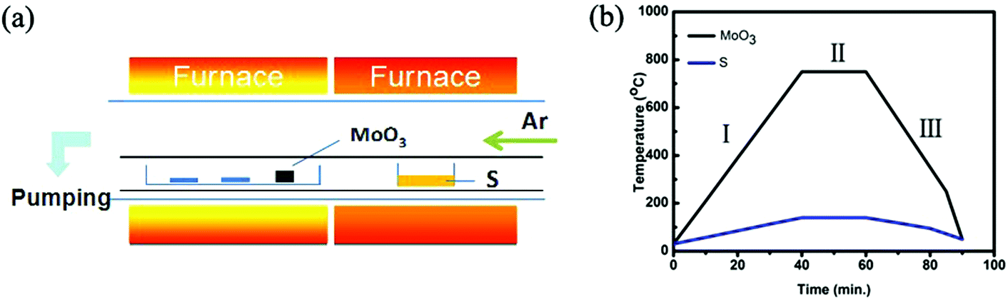 | ||
| Fig. 1 (a) Schematic illustration of the CVD system for MoS2 synthesis. (b) Temperature programming process of MoO3 and S precursors. | ||
Fig. 2 presents the typical scanning electron microscopy (SEM) images of nearly round (Fig. 2a) and round (Fig. 2b) MoS2 domains. With the increase in the growth time from 20 min to 45 min, the grains tended to grow larger (Fig. 2a and b) and merged together to form a continuous MoS2 film (Fig. 2c). The round-shaped MoS2 domains are strikingly different from previous observation of triangle-shaped MoS2 domains. Moreover, except for the few smaller domains, the large domains of the same sample have an identical size, exhibiting high homogeneity. Fig. 2d shows a representative atomic force microscopy (AFM) topographic image of the round MoS2 domains and the cross-sectional profile (Fig. 2e) depicts that the thickness of the domain is about 0.69 nm, corresponding to one MoS2 atomic layer. At this moment, we do not know the composition of the random white dots on some of the domains (Fig. 2d), which might be a contaminant, intermediate product of the reaction or nucleation seed. The high-resolution transmission electron microscopy (HRTEM) image in Fig. 2f clearly reveals the periodic atom arrangement of the MoS2 domain with typical (100) and (110) interplanar spacings of 0.27 and 0.16 nm, respectively.
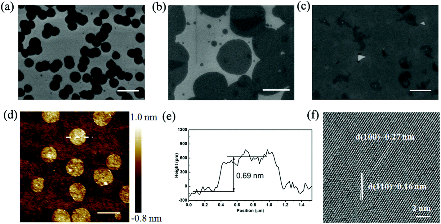 | ||
| Fig. 2 Structural characterization of (nearly) round-shaped monolayer MoS2 synthesized at 750 °C. (a) SEM images of MoS2 domains grown for 20 min. (b) SEM images of MoS2 domains grown for 30 min. (c) SEM images of MoS2 domains grown for 45 min. Scale bar in (a)–(c): 1.0 μm. (d) AFM image, scale bar: 1.0 μm. (e) The height profile taken across the dotted line in (d). (f) HRTEM images of round MoS2. | ||
Raman spectroscopy was employed to characterize the vibration mode of Mo–S, further to determine the layer number of the round MoS2 domains. Fig. 3a shows the Raman spectra obtained from the MoS2 domains with sizes of about 200 nm, 400 nm and 700 nm (see Fig. 4a–c), respectively. The in-plane vibration named E2g1 mode is located at 386.0 cm−1, and the A1g mode representing the out-of-plane vibration is at 406.0 cm−1.25 Furthermore, the frequency difference between the two characteristic peaks is 20.0 cm−1 in each spectrum, which reveals that the domains with different sizes are all monolayer.26Fig. 3c and d represent the intensity mappings of A1g and E2g1 modes of a sample different from those characterized in Fig. 3a and b, respectively. Both mappings show a similar landscape; the mappings exhibit a uniform intensity distribution, except for the slightly weaker intensity at the edges which might be defective edges or the large laser beam (∼1 μm) used for the measurement. The mappings provide more accurate characterization and better resolution for the atomic layer samples with a possible change of the thickness. The Raman characteristics strongly suggest the good quality of the MoS2 monolayer on the SiO2 substrate, which is manifested by the photoluminescence (PL) mapping in Fig. 3e.
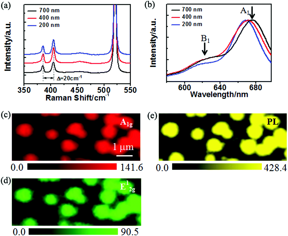 | ||
| Fig. 3 (a) Raman spectra obtained from different-sized (i.e., about 200 nm, 400 nm and 700 nm) MoS2 domains. (b) Normalized PL spectra obtained from different-sized (i.e., about 200 nm, 400 nm and 700 nm) MoS2 domains. (c) and (d) Raman mapping of the peak intensity of A1g and E2g1, respectively. (e) PL intensity mapping. | ||
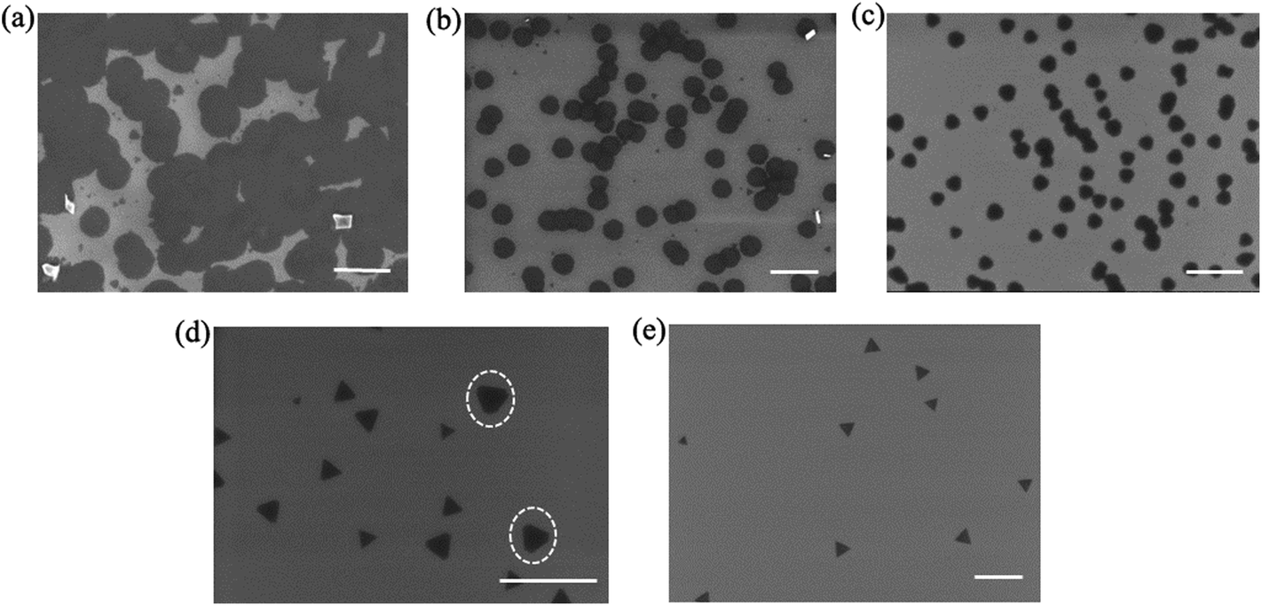 | ||
| Fig. 4 SEM images of MoS2 domains grown for 20 min at different temperatures of the MoO3 precursor. (a)–(e) Temperature was 760, 750, 730, 720 and 710 °C, respectively. The domain size in (a)–(c) is about 700 nm, 400 nm and 200 nm, respectively. Scale bar in (a)–(e): 1.0 μm. | ||
According to the band structure calculation and previous experimental studies,8–10 MoS2 undergoes a transformation from an indirect band gap to a direct band gap as the thickness is thinned down to a single layer. As a result, the PL intensity is dramatically enhanced in monolayer MoS2 compared to bulk and few-layer MoS2. Fig. 3e illustrates the PL mapping of the round MoS2 domains, showing a homogeneous PL intensity distribution of the monolayer domains. The considerable PL intensity of the round MoS2 domains is another proof of monolayer characteristics of the MoS2 domains. The normalized PL spectra from the different-sized MoS2 domains are presented in Fig. 3b. It is found that the PL emission peak related to A1 excitation is located at 675.0 nm, 670.0 nm and 668.0 nm for the 700 nm, 400 nm and 200 nm domains (see Fig. 4a–c), respectively. The observed blue shift of the peaks of A1 excitation as well as B1 excitation (about 620 nm) with a decrease in the domain size may be due to the doping or strain effect at the grain boundary with a variable grain boundary density.19,24 In general, the doping or strain around the grain boundary may change the charge density and modulate the band structure of MoS2. First, local doping arises from the lattice vacancies and adsorbates at the boundaries.19 The charge density change at the grain boundary results in PL quenching/enhancement.27 The influence of charge thus may provide an explanation for the intensity variation at the grain boundaries as observed in the PL mapping (Fig. 3e). Additionally, doping might induce gap states and influence carrier recombination. Second, the strain around the boundary may modify the band gap and in turn shift the emission energy.19,28,29 It was reported that the strain can give rise to a blue shift of the MoS2 band gap28 by effectively changing the energy difference between the K and Q valleys.29 In the case of smaller domains, more domain boundaries and a higher boundary density are involved in the area of laser excitation. Hence, a blue shift occurred in the small MoS2 domains as compared to the large domains.
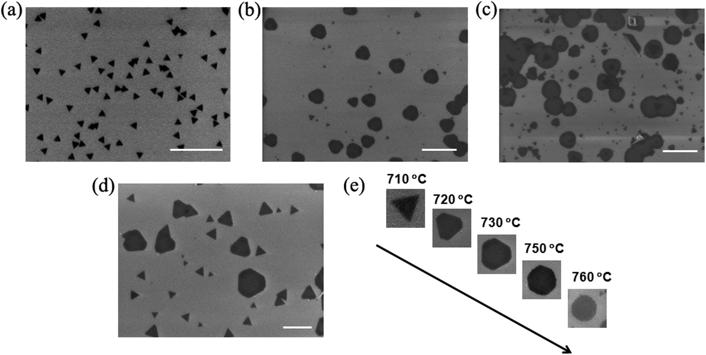
We can also generate triangle MoS2 domains by adjusting the evaporation temperature of the MoO3 and S precursors, translating to control the precursor concentrations at a fixed volume of the quartz tube. Fig. 4 depicts the SEM images acquired from the samples which were synthesized at different temperatures of the MoO3 precursor. A closer examination reveals the shape difference of the MoS2 domains synthesized at different temperatures. We found that the MoS2 domains are mainly round, nearly round and hexagonal, and truncated triangles grown at 760 °C (Fig. 4a), 750 °C (Fig. 4b) and 730 °C (Fig. 4c), respectively. However, the domain size became smaller, i.e., about 700 nm, 400 nm and 200 nm, with the decrease in the temperature from 760 °C to 730 °C, respectively. At 710 °C, we produced triangle MoS2 domains (Fig. 4e), and the domain density is lower and the size is smaller than those obtained at a higher temperature. Even though the growth time was extended from 20 min to 40 min at 710 °C, the triangle MoS2 domain shape is maintained (see the ESI, Fig. S5†); the size of the domains is slightly larger than those grown for 20 min. This is because the evaporation rate of the MoO3 was too low, resulting in a very low reaction rate. The observation justifies the present discussion. Furthermore, at 720 °C, truncated triangles appeared in addition to the triangle MoS2 domains, and the size of the truncated triangle domains is larger than that of the triangles (Fig. 4d). The difference in size indicates the transformation from a triangle to a truncated triangle, which also reflects the influence of the reaction rate on the shape of MoS2 domains. These observations suggest that the sharp transition point from a thermodynamic growth regime to a kinetic growth regime as discussed later occurred at about 720 °C under the present experimental conditions.
Triangle is the most commonly observed shape of MoS2 domains because of the hexagonal symmetry,30 while round-shaped MoS2 domains have been rarely observed.24 The driving force for the anisotropic growth of crystals is originated from the thermodynamic stabilization of the given facets of crystals. Since the crystalline growth rate varies exponentially with the surface free energy which corresponds to the edge free energy in 2D crystals,23 the selective adsorption of atoms on a given crystallographic facet can inhibit the growth rate along one particular crystallographic direction, leading to a preferential growth along another (or other) direction(s) and to the formation of distinct shapes. The low-energy facets tend to grow slowly.
The formation of MoS2 domains involves dynamic processes of the precursor evaporation, precursor transport and precursor reaction. One should also consider the chemical reaction which occurred before and after the assumed growth stage (i.e., the II stage in Fig. 1b) because substantial precursor evaporation and mass transfer could happen at lower temperatures i.e., at the I and III stages in Fig. 1b, than the reaction temperature intentionally set for the growth. Initially, thermodynamically stable triangle nuclei formed randomly because the reactants existed and the concentration of the reactants (Mo and S) was low enough for a thermodynamically favored process according to classic crystal growth theory. This is further evidenced by our terminated growth. In this investigation, we stopped the heating at 690 °C before the temperature had reached the set evaporation temperature of 750 °C of the MoO3 precursor. As observed in Fig. 5a, triangle-shaped MoS2 domains were produced. This suggests that the nuclei had already formed prior to the designed growth stage. In a thermodynamically controlled growth regime, the reactive Mo and S atoms absorb onto the substrate surface and then diffuse to the energetically favorable location, leading to the formation of stable triangles. Such a growth regime is achieved in the presence of a relatively low reactant concentration of Mo and S atoms. In this study, such a thermodynamic controlled growth regime occurred before the temperature reached 730 °C.
 | ||
| Fig. 5 SEM images of MoS2 domains grown under different conditions. (a) The heating process was shut down at 690 °C before the set temperature reached 750 °C. (b) Grown for 5 min at a temperature of 750 °C. (c) With a lower cooling rate of about 5 °C min−1 in contrast to a normal cooling rate of about 10 °C min−1. (d) Different-shaped MoS2 domains grown for 20 min at 750 °C without the small inner tube as shown in Fig. 1a. Scale bar in (a)–(d): 1.0 μm. (e) Shape evolution of MoS2 domains as a function of temperature. | ||
An appropriate choice of experimental conditions can shift a thermodynamic-controlled growth regime to a kinetic-controlled growth regime. This concept of kinetic shape control is directly dependent on the reaction rate (i.e., growth rate), which depends on the reactant concentration in the reaction environment. Under the environment of evaporation temperature of 730 °C or above and the nearly closed quartz tube, the reactants rapidly accumulated as the temperature increased, which led to a higher reaction rate beyond the thermodynamic equilibrium regime and turned the reaction to a kinetic controlled condition. In the kinetic regime, the Mo and S adatoms did not have sufficient time to diffuse to the favorable sites with the lowest energy but to a lower energetic position. It is known that the round shape has the smallest perimeter to the area ratio, which indicates that with the same number of atoms, less atoms are exposed outside and the dangling bonds reduce. Therefore, the initial triangle nuclei transformed into round MoS2 domains via a truncated triangle. The deviation from the thermodynamic equilibrium is thus due to the high reaction rate driving the Mo and S atoms to finally form a round shape. Note that the substrate temperature increased together with the increase in the temperature of the MoO3 precursor. The substrate temperature increase enhanced the diffusion of reactive Mo and S atoms on the substrate, which should drive the growth to a thermodynamically favored process and result in triangle domains. However, regularly triangle MoS2 domains were not formed at the elevated substrate temperatures in our experiments. This reflects that the reaction rate is the limiting factor dominating the growth of MoS2.
On the other hand, if the growth time, i.e., the evaporation time of precursors, was reduced to only 5 min as compared to normal 20 min, we observed very small triangles and the transformation of triangles to truncated triangle MoS2 domains even at the evaporation temperature of 750 °C (Fig. 5b). This is because the reactant accumulation had not yet fully reached the critical value for a kinetic controlled growth. That is, the growth was at the interim of the transformation. When the average cooling rate became lower (from about 10 °C min−1 to 5 °C min−1) after the growth, small triangle MoS2 domains were formed on the substrate and on the already grown round MoS2 surface (see Fig. 5c). This is because the reactant concentration remaining in the quartz tube became lower with the cooling process than at the growth stage. The final shape, thus, could be the result of a balance between the nucleation and growth rates which govern the thermodynamics and kinetics effects.
For a comparison, we synthesized MoS2 domains with a common single quartz tube CVD system. That is, we carried out the synthesis without the small inner tube as used in Fig. 1a. As shown in Fig. 5d, the shapes of the MoS2 domains grown at 750 °C are triangle and truncated triangle. Furthermore, the size of the triangles varied much. The formation of such shapes is due to a lower reactant concentration in the large tube than that in the small tube. The different-sized triangles may be due to the fluctuation of the reactant atmosphere in the large tube, suggesting the advantage of our dual-tube configuration for the achievement of fine control over the reactive atmosphere. The observed different shapes illustrate the evolution of MoS2 domains from triangle to truncated triangle, hexagonal, and finally round shape (Fig. 5e). Although a change of MoS2 domains was observed from triangle to truncated triangle and hexagonal shape,23 no transformation has been observed in the round-shaped MoS2 domain. And the reported shape evolution was attributed to the alternation of the Mo![[thin space (1/6-em)]](https://www.rsc.org/images/entities/char_2009.gif) :S atom ratio in the thermodynamic-controlled growth regime stemming from the variation of the distance between the MoO3 precursor and the substrate.23 We also observe the shape change as a function of the distance (see Fig. S4 in the ESI†), which indicates that there exists the optimal distance for the growth of the uniform MoS2 domains and in our case was about 4–6 cm between the MoO3 precursor and the substrate.
:S atom ratio in the thermodynamic-controlled growth regime stemming from the variation of the distance between the MoO3 precursor and the substrate.23 We also observe the shape change as a function of the distance (see Fig. S4 in the ESI†), which indicates that there exists the optimal distance for the growth of the uniform MoS2 domains and in our case was about 4–6 cm between the MoO3 precursor and the substrate.
We further evaluate the electrical properties of the MoS2 monolayers with round domains by fabricating back-gate field-effect transistors (FETs). We fabricated 15 FETs by photolithography and lift-off techniques.31 The channel length and width of our devices were 4.0 μm and 6.0 μm, respectively. All the devices exhibited n-type behavior. Fig. 6 shows the transfer and output characteristics of a typical device. The calculated room-temperature electron mobility and the on/off ratio of the device are 1.05 cm2 V−1 s−1 and 1.20 × 10⁵, respectively. The average mobility over the 15 devices is 0.95 cm2 V−1 s−1 ranging from 0.74 to 1.39 cm2 V−1 s−1. Although the domain size is small as compared to most reported triangle domains, the mobility values of our devices fabricated with the continuous film consisting of the round MoS2 domains are in the range of the reported values for back-gated FETs fabricated with mechanically exfoliated MoS2 on SiO2 (0.1–10.0 cm2 V−1 s−1).8 The on/off ratio of our devices is relatively lower than most reported values. The reasons may be the existence of mid-gap states localized at the boundary and the leakage current due to damage to the SiO2 dielectric layer during the MoS2 synthesis. The localized mid-gap states in the MoS2 films could affect the transport properties of the films,19 and the leakage current increased the off-current.
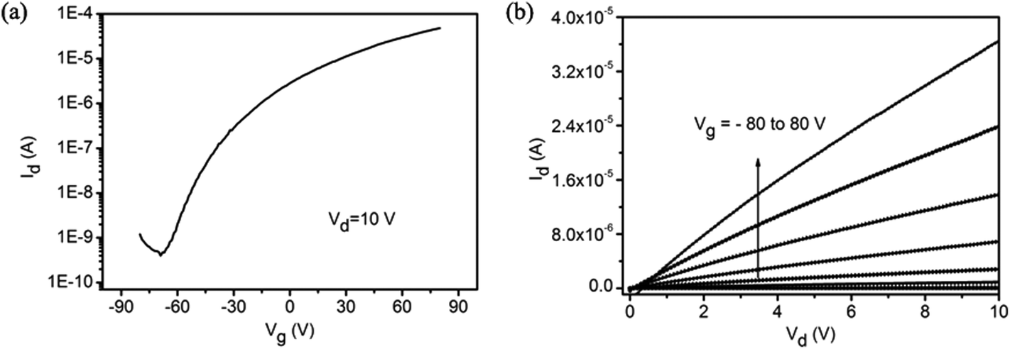 | ||
| Fig. 6 Electrical characteristics of MoS2 monolayers constructed with round domains. (a) Transfer curve for the FET device. (b) Output curve for the FET device. | ||
Conclusions
We have demonstrated the production of round-shaped monolayer MoS2 domains with a tunable size and the transformation from triangle to round MoS2 domains by using the CVD system with dual-quartz tubes. The field-effect mobility and the on/off ratio of the grown MoS2 monolayer are up to 1.39 cm2 V−1 s−1 and ∼105, respectively. We found that it is possible to realize either the thermodynamic growth regime or the kinetic growth regime for the preparation of MoS2 by controlling the growth rate which highly relies on the concentration of reactants. The shift of the growth regime allowed us to transform the triangle MoS2 nuclei into the round MoS2 domains. Furthermore, our study reveals the dominant factors that influence the synthesis of MoS2 and improves our understanding of the nucleation and growth mechanisms of MoS2, towards fine control over the synthesis of MoS2 and other TMDs.Author contributions
X. M. and M. X. supervised the project; M. X. conceived and designed the experiments; S. X. carried out growth experiments and measurements with the assistance of T. L., G. H., S. W. and G. X. under the supervision of X. M. and M. X.; N. M. fabricated the FETs under the supervision of Y. X.; M. X. and S. X. analysed the data and wrote the manuscript; X. M., H. C. and D. Y. discussed the results and commented on the manuscript.Acknowledgements
This work was supported by the 973 Program (2013CB632102), the Program for New Century Excellent Talents in University (NCET-12-0494), the Research Fund for the Doctoral Program of Higher Education (20130101110123), the Program for 14th China-Japan S&T Cooperation (2013DFG52800), the National Natural Science Foundation of China (no. 51472219, 51450110082, 61274123, 61474099), and the Zhejiang Provincial NSF (no. R4110030, LR12F04001). The authors would also like to acknowledge the financial support by the Innovation Platform of Micro/Nano devices and Integration System at Zhejiang University. S. Xie is supported by the Zhejiang University Lu Graduate School Student Education Foundation for International Exchange. Y. Xu is supported by the ZJU Cyber Scholarship, the Cyrus Tang Center for Sensor Materials and Applications, and a Visiting-by-Fellowship of Churchill College, University of Cambridge.Notes and references
- M. S. Xu, T. Liang, M. M. Shi and H. Z. Chen, Chem. Rev., 2013, 113, 3766 CrossRef CAS PubMed.
- A. K. Geim and K. S. Novoselov, Nat. Mater., 2007, 6, 183 CrossRef CAS PubMed.
- M. S. Xu, D. Fujita, K. Sagisaka, E. Watanabe and N. Hanagata, ACS Nano, 2011, 5, 1522 CrossRef CAS PubMed.
- M. S. Xu, D. Fujita, H. Z. Chen and N. Hanagata, Nanoscale, 2011, 3, 2854 RSC.
- X. Yang, W. F. Fu, W. Q. Liu, J. H. Hong, Y. Cai, C. H. Jin, M. S. Xu, H. B. Wang, D. R. Yang and H. Z. Chen, J. Mater. Chem. A, 2014, 2, 7727 CAS.
- P. Vogt, P. D. Padova, C. Quaresima, J. Avila, E. Frantzeskakis, M. C. Asensio, A. Resta, B. Ealet and G. L. Lay, Phys. Rev. Lett., 2012, 108, 155501 CrossRef PubMed.
- R. Wang, X. D. Pi, Z. Y. Ni, Y. Liu, S. S. Lin, M. S. Xu and D. R. Yang, Sci. Rep., 2013, 3, 3507 Search PubMed.
- K. F. Mak, C. G. Lee, J. Hone, J. Shan and T. F. Heinz, Phys. Rev. Lett., 2010, 105, 136805 CrossRef PubMed.
- H. L. Zeng, J. F. Dai, W. Yao, D. Xiao and X. D. Cui, Nat. Nanotechnol., 2012, 7, 490 CrossRef CAS PubMed.
- X. D. Xu, W. Yao, D. Xiao and T. F. Heinz, Nat. Phys., 2014, 10, 343 CrossRef CAS.
- B. Radisavljevic and A. Kis, Nat. Mater., 2013, 12, 815 CrossRef CAS PubMed.
- S. F. Wu, S. Buckley, J. R. Schaibley, L. F. Feng, J. Q. Yan, D. G. Mandrus, F. Hatami, W. Yao, J. Vučković, A. Majumdar and X. D. Xu, Nature, 2015, 520, 69 CrossRef CAS PubMed.
- Y. Cai, X. Yang, T. Liang, L. Dai, L. Ma, G. W. Huang, W. C. Chen, H. Z. Chen, H. X. Su and M. S. Xu, Nanotechnology, 2014, 25, 46504 Search PubMed.
- C. F. Zhu, Z. Y. Zeng, H. Li, F. Li, C. H. Fan and H. Zhang, J. Am. Chem. Soc., 2013, 135, 5998 CrossRef CAS PubMed.
- X. Yang, J. Li, T. Liang, C. Y. Ma, Y. Y. Zhang, H. Z. Chen, N. Hanagata, H. X. Su and M. S. Xu, Nanoscale, 2014, 6, 10126 RSC.
- Y. M. Shi, H. N. Li and L.-J. Li, Chem. Soc. Rev., 2015, 44, 2744 RSC.
- Q. Q. Ji, Y. Zhang, Y. F. Zhang and Z. F. Liu, Chem. Soc. Rev., 2015, 44, 2587 RSC.
- K. Kang, S. Xie, L. J. Huang1, Y. M. Han, P. Y. Huang, K. F. Mak, C. J. Kim, D. Muller and J. W. Park, Nature, 2015, 520, 656 CrossRef CAS PubMed.
- A. M. van der Zande, P. Y. Huang, D. A. Chenet, T. C. Berkelbach, Y. M. You, G.-H. Lee, T. F. Heinz, D. R. Reichman, D. A. Muller and J. C. Hone, Nat. Mater., 2013, 12, 554 CrossRef CAS PubMed.
- Y.-H. Lee, L. L. Yu, H. Wang, W. J. Fang, X. Ling, Y. M. Shi, C.-T. Lin, J.-K. Huang, M.-T. Chang, C.-S. Chang, M. Dresselhaus, T. Palacios, L.-J. Li and J. Kong, Nano Lett., 2013, 13, 1852 CAS.
- S. F. Wu, C. M. Huang, G. Aivazian, J. S. Ross, D. H. Cobden and X. D. Xu, ACS Nano, 2013, 7, 2768 CrossRef CAS PubMed.
- S. Najmaei, Z. Liu, W. Zhou, X. L. Zou, G. Shi, S. D. Lei, B. I. Yakobson, J.-C. Idrobo, P. M. Ajayan and J. Lou, Nat. Mater., 2013, 12, 754 CrossRef CAS PubMed.
- S. S. Wang, Y. M. Rong, Y. Fan, M. Pacios, H. Bhaskaran, K. He and J. H. Warner, Chem. Mater., 2014, 26, 6371 CrossRef CAS.
- J. Zhang, H. Yu, W. Chen, X. Z. Tian, D. H. Liu, M. Cheng, G. B. Xie, W. Yang, R. Yang, X. D. Bai, D. X. Shi and G. Y. Zhang, ACS Nano, 2014, 8, 6024 CrossRef CAS PubMed.
- C. G. Lee, H. G. Yan, L. E. Brus, T. F. Heinz, J. Hone and S. Ryu, ACS Nano, 2010, 4, 2695 CrossRef CAS PubMed.
- H. Li, Z. Y. Yin, Q. Y. He, H. Li, X. Huang, G. Lu, D. W. H. Fam, A. I. Y. Tok, Q. Zhang and H. Zhang, Small, 2012, 8, 63 CrossRef CAS PubMed.
- K. F. Mak, K. L. He, C. Lee, G. H. Lee, J. Hone, T. F. Heinz and J. Shan, Nat. Mater., 2013, 12, 207 CrossRef CAS PubMed.
- L. Yang, X. Cui, J. Zhang, K. Wang, M. Shen, S. Zeng, S. A. Dayeh, L. Feng and B. Xiang, Sci. Rep., 2014, 4, 5649 CAS.
- Y. Ge, W. Wan, W. Feng, D. Xiao and Y. Yao, Phys. Rev. B: Condens. Matter, 2014, 90, 035414 CrossRef.
- S. Helveg, J. V. Lauritsen, E. Lagsgaard, I. Stensgaard, J. K. Norskov, B. S. Clausen, H. Topsoe and F. Besenbacher, Phys. Rev. Lett., 2000, 84, 952 CrossRef PubMed.
- M. S. Xu, M. Nakamura, M. Sakai and K. Kudo, Adv. Mater., 2007, 19, 371 CrossRef CAS.
Footnote |
| † Electronic supplementary information (ESI) available. See DOI: 10.1039/c5nr05701a |
| This journal is © The Royal Society of Chemistry 2016 |