
Derivation of the surface free energy of ZnO and GaN using in situ electron beam hole drilling†
Jay
Ghatak
*ab,
Jun-Han
Huang
b and
Chuan-Pu
Liu
b
aInternational Center for Materials Science, Jawaharlal Nehru Centre for Advanced Scientific Research, Jakkur, Bangalore 560064, India. E-mail: jayghatak@jncasr.ac.in
bDepartment of Materials Science and Engineering, National Cheng Kung University, Tainan City 701, Taiwan
First published on 10th November 2015
Abstract
Surface free energy, as an intrinsic property, is essential in determining the morphology of materials, but it is extremely difficult to determine experimentally. We report on the derivation of the SE of different facets of ZnO and GaN experimentally from the holes developed using electron beam drilling with transmission electron microscopy. Inverse Wullf's construction is employed to obtain polar maps of the SE of different facets to study different nanomaterials (ZnO and GaN) in different morphologies (nanorod, nanobelt and thin film) to prove its versatility and capability. The results show that the SE of ZnO{10−13} is derived to be 0.99 J m−2, and the SE of ZnO{10−10} is found to be less than {0002} and {11−20}. A GaN thin film also exhibits a similar trend in the SE of different facets as ZnO and the SE of GaN{10−13} is determined to be 1.36 J m−2.
1. Introduction
As a result of the move toward lighter and smaller futuristic devices, various growth techniques have been developed for the synthesis of low dimensional materials with various morphologies. There are top down approaches based on focused ion beam or other dry etching processes, but these techniques are expensive and complicated. On the other hand, bottom up approaches, such as vapour growth using chemical vapour deposition etc. or solution chemistry growth using hydrothermal synthesis, sol–gel processes etc., rigorously rely on a nucleation and growth mechanism and are mostly governed by the thermodynamics of the system. Hence controlled growth of the desired morphologies of materials (mostly semiconductors for micro-electronics) demands sufficient knowledge of the surface free energies (SEs) of the materials. The SEs of solid metals have been estimated from liquid surface tension measurements.1,2 Specific SEs of Ge and Si were measured using a cleavage technique.3 The SEs of various planes in Si, GaAs, and GaP were measured using a modified spark discharge method.4 Most of the studies estimated the average SE instead of the SE of individual planes. Moreover, these studies were made on bulk materials. As the physics of bulk materials differs from their nanomaterial counterparts, finding out the SEs of nanomaterials becomes essential. SEs are surface related properties and require an ultra-clean environment for carrying out the measurements. Difficulties may also arise from the contamination of the surfaces of nanomaterials during synthesis, handling and sample preparation. But the present techniques for determining SE demand self-supported nanostructures in an ultra clean-environment, which are almost impossible to have for these experiments. This is true for any kind of material to be synthesised and analysed. Among them, ZnO and GaN represent two typical model materials widely employed in optoelectronics, where there is plenty of research carried out on the growth mechanisms and properties of nanomaterials in various forms. Unfortunately, in spite of extensive discussion based on SEs, there are no experimental derivations of the SE in any form yet probably due to the above-mentioned difficulties. There are also scarce theoretical data about SE studies on these materials available (Table 1). One of them reported the SEs of ZnO as 1.91{0001}, 1.01{10−10}, 1.57{10−11} and 1.02{11−20} J m−2 and SEs of GaN as 2.64{0001}, 1.40{10−10}, 1.76{10−11} and 1.53{11−20} J m−2 using ab initio calculations.9 But the interpretation is tricky since SE is sensitive to the environment (temperature, presence of foreign molecules etc.) on which the surface has been exposed. On the other hand, the theoretical data are scattered (as shown in Table 1) as they depend on assumptions employed in the simulations that lead to results sometimes not even close to the reality.6| Material | Surface free energy (J m−2) | Ref. | |||
|---|---|---|---|---|---|
| (0001) | (10−10) | (10−11) | (11−20) | ||
| a Calculated based on half of the cleavage energy. | |||||
| ZnOa | 2.70 | 1.16 | 2.05 | 5 | |
| ZnOa | 2.15 | 1.15 | — | 1.25 | 6 |
| ZnO | 1.58 | 0.91 | 1.64 | 1.64 | 7 |
| ZnO | 2.25 | 1.12 | 1.06 | 8 | |
| ZnO | 1.91 | 1.01 | 1.57 | 1.02 | 9 |
| ZnOa | 1.96 | 1.05 | — | 1.01 | 10 |
| GaN | — | 1.95 | — | 3.50 | 11 |
| GaN | — | 1.61 | — | 1.68 | 12 |
| GaN | 2.64 | 1.40 | 1.76 | 1.53 | 9 |
It has been more than a century since Wullf postulated that the equilibrium shape of a material can be determined from the knowledge of the polar plot of SEs.13,14 Hence, in other words, the SE of individual facets can be derived experimentally if the equilibrium shape of the material is achieved, which is called “inverse Wulff's construction”. It has been difficult to grow stand-alone equilibrium structures under controlled conditions either using top-down (e.g. focused ion beam) or bottom up approaches (e.g. hydrothermal and physical vapour disposition growth techniques) to find out SEs using this process. Therefore, alternative methods for getting equilibrium structures must be developed. One such method has been demonstrated by Eaglesham et al. where they determined the SEs of several facets of Si from the equilibrium shape of voids formed using MeV He ion implantation followed by annealing using inverse Wulff's construction.15 Follstaedt et al. calculated the relative SE of various surfaces of Si from the voids formed by ion implantation using the similar procedure.16 In our previous report, the SE was derived from nanopores inside single crystalline ZnO nanorods, synthesised using a hydrothermal process followed by optimized heat treatment, and the average SE of ZnO{10−13} was found to be ≈0.99 J m−2 using “Inverse Wulf's construction”.17 With the advancement of technology, modern transmission electron microscopes have gone beyond microscopy to spectroscopy including probing single atoms18,19 and the study of localised magnetic moments20 and electronic structures21etc. In this report, with the help of electron beam drilling during TEM, one more fundamental function of TEM will be established, allowing the SEs of different facets of materials to be determined qualitatively as well as quantitatively in a clean environment under vacuum ≈10−8 mbar (in situ TEM) and we believe that this will open up a new field where the SE, an important intrinsic property, of many unknown materials can be measured.
2. Experiments
Single crystalline ZnO nanorods with a growth direction of [0002] were synthesized using a hydrothermal process. The details of the synthesis procedure have been reported elsewhere.17 In-plane ZnO nanobelts with a growth direction of [10−10] on a silicon substrate were grown using a vapour transport method in an Ar/O2 atmosphere. Firstly, Ar of about 8 sccm was introduced at increasing temperatures up to 650 °C for 30 min using zinc powder as the source. At this temperature (650 °C), O2 of about 1 sccm was also introduced and held for 1 h. After cooling down, ZnO nanobelts were scratched off and dispersed on carbon coated copper grids for further experiments using TEM. A GaN thin film was grown using metal–organic vapour phase epitaxy (MOVPE) on a c-place sapphire and details of the growth procedure and cross-sectional TEM sample preparation can be found elsewhere.22 Electron beam hole drilling experiments were carried out in situ with 200 kV and 300 kV electrons using TEM, performed on JEOL 2100F, FEI Tecnai T20 and FEI Titan microscopes. The diversity of microscopes used was just subject to availability, however, electron energy and beam current certainly play crucial roles in the experiments and will be discussed in the following sections.3. Experimental results
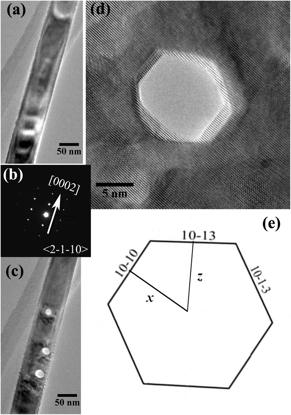
In this study, two different materials (ZnO and GaN) with various morphologies (nanorod, nanobelt and thin film) have been considered. Each of them was irradiated in situ with energetic (200 or 300 keV) electrons that are available in the transmission electron microscope with the beam converged to achieve the highest beam current. All the samples were tilted to the nearest zone axis prior to irradiation to gain accurate information on the facets developed due to beam damage.For the first set of experiments, ZnO nanorods 40 nm in diameter grown using a hydrothermal process were tested. The details of growth conditions with characterization of the morphology and chemical composition have been previously reported.17Fig. 1(a) shows a hole created in one of the ZnO nanorods upon irradiation with 200 keV electrons (JEOL 2100F) for about 1 min with ≈100 pA total beam current. The nanorod was tilted to the <2−1−10> zone axis prior to irradiation and the electron diffraction (ED) pattern is shown in the inset of Fig. 1(a). From the ED pattern, the facets can easily be identified as {10−10}, {10−13} and {0002}, as shown in the schematic diagram of the drilled hole in Fig. 1(b). Here, x represents the distance between the Wulff center and midpoint of facet (10−10) (perpendicular bi-sector from the Wulff point). Similarly, w and z are the corresponding distances measured for (10−13) and (0002), respectively. If we recall “Wulff's construction”, then the values of z/x and x/w are equal to γz/γx and γx/γw (where γi is the surface free energy of the ith facet). In this shape, the ratio of z/x = γz/γx = 1.14 and x/w = γx/γw = 0.94. If we consider γx = 1.01 J m−2,9 then γz = 1.15 J m−2 and γw = 1.07 J m−2, which means for this shape the SE of (10−13) is higher than that estimated using a different approach in our previous report.17 Even the ratio of γ(10−10) to γ(0002) of 0.94 (as the SE of (0002) is 1.07 J m−2) is much higher than the predicted theoretical value (≈ 0.5) (see Table 1). Hence, it can be concluded that the hole shape shown in Fig. 1(b) is not the thermodynamic equilibrium shape of ZnO. This could be due to insufficient energy to knock-out atoms (sputtering) and/or an insufficient number of electrons at this beam current, which is also responsible for a higher beam heating effect. The effect of beam energy and beam current will be discussed in the subsequent section. A longer irradiation time of more than 5 min has been attempted using the same transmission electron microscope to make more electrons available to sputter the atoms, but the perforated equilibrium shape is still not reached partly due to the instability of the sample (mechanical drift).
 | ||
| Fig. 1 (a) TEM image of a hole created in a ZnO nanorod upon 200 keV electron beam irradiation; inset shows the diffraction pattern along the <2−1−10> zone axis. (b) Schematic diagram of the hole with the facets identified as {10−10}, {10−13} and {0002}. | ||
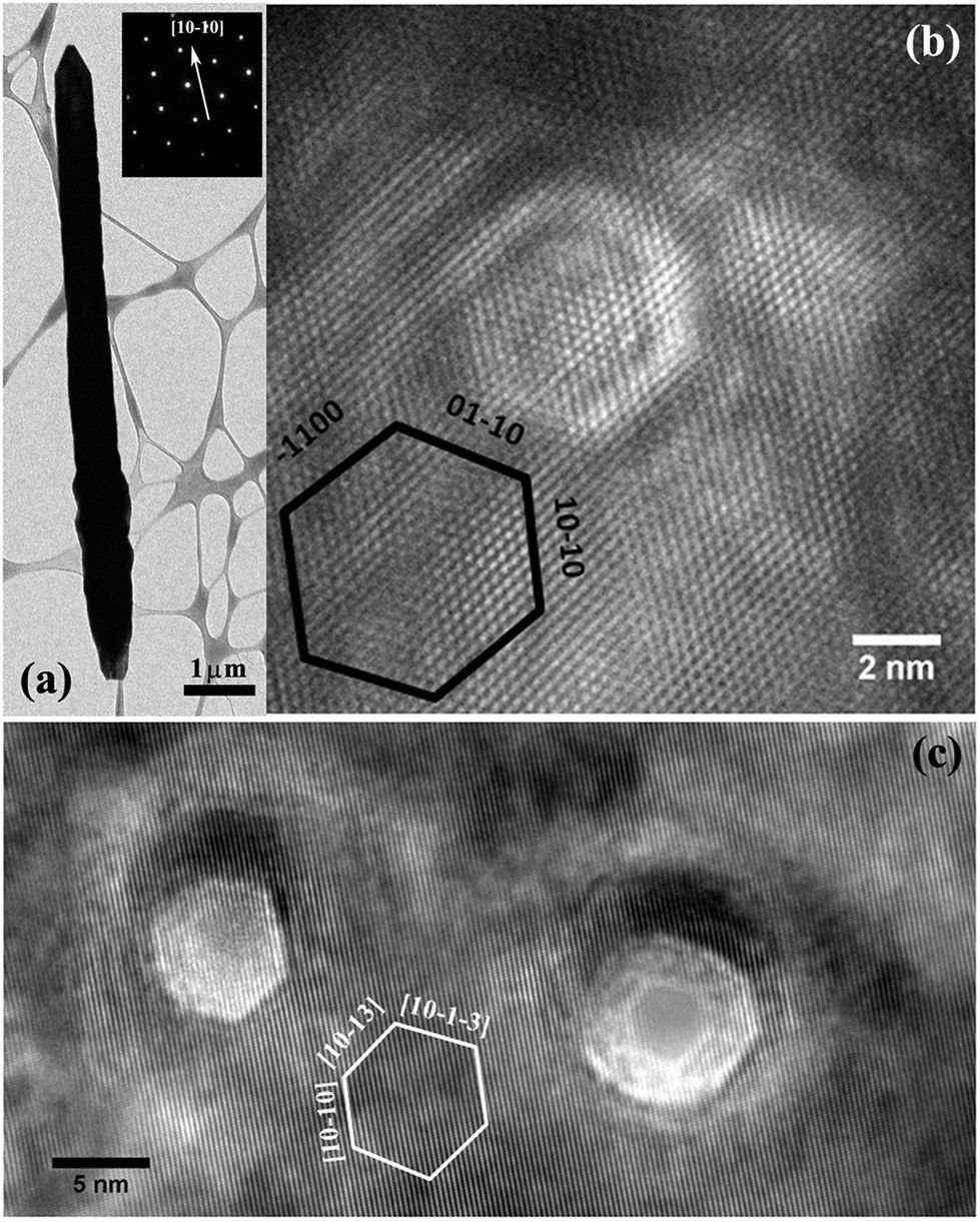
To improve the results, a 300 keV transmission electron microscope (FEI TITAN 80-300) was then used to carry out similar experiments on the same ZnO nanorod. Fig. 2(a) is the TEM image of the ZnO nanorod (the same nanorod as used in the experiments shown in Fig. 1) before irradiation and Fig. 2(b) shows the ED pattern of the ZnO nanorod tilted to the <2−1−10> zone axis. Irradiation was then carried out in several different regions of the nanorod, each for about a minute with ≈7 nA beam current, and the result is shown in Fig. 2(c). Fig. 2(d) shows one of the holes at higher magnification and it is now to be noticed that, unlike the previous case using 200 keV irradiation, the hole penetrates through the nanorod completely and exhibits a hexagonal instead of octagonal shape. From the ED pattern, the facets are identified as being composed only of {10−10} and {10−13} with the {0002} facet missing, as the schematic diagram shows in Fig. 2(e). This shape is identical to that of the other holes developed in Fig. 2(c) and also to what was achieved in our previous studies through annealing experiments.17 It is to be noted that similar holes were not achieved when bombarded with 200 kV electrons. This proves that holes of equilibrium shapes could be realized in this case using a higher electron energy (hence a higher rate of sputtering), more electrons available for this beam current (flux which causes higher beam heating effect) along with somewhat better sample stability (suitable for a longer irradiation time). Overall, the supplied energy (by momentum transfer and beam heating effect) to the target atoms must be sufficient to achieve equilibrium shape. The irradiation conditions to achieve the equilibrium shape may vary from material to material. It is to be noted that the absence of the {0002} facet suggests that the SE of this facet is much larger than that of {10−10} and {10−13}, which is also supported by the theoretical results. The role of electron energy in hole drilling will be discussed in the subsequent section.
 | ||
| Fig. 2 (a) TEM image of a ZnO nanorod before irradiation. (b) Diffraction pattern from the nanorod along <2−1−10> zone axis. (c) TEM image of holes created upon 300 keV electron beam irradiation. (d) Magnified image of one of the holes. (e) Schematic diagram of the hole with the facets identified as {10−10} and {10−13}. | ||
Following the work of Eaglesham et al.15 and our previous report,17Fig. 2(e) can be considered as the equilibrium Wulff shape, representing the polar plot of r(i) versus θ where r(i) is the relative hole radius (from the centre to any point on the boundary of the hole) and θ is measured at the position of r(i) with respect to any arbitrary r in that shape as θ = 0 (details are given in the “ESI†”). Again we have assumed that the internal void shape is identical to the external crystal shape (as mentioned in ref. 15 and 17). In Fig. 3, the r(i) at different points on the shape is plotted from the intersection of the perpendicular bisector of two different facets (Wulff point or center of mass) with ≈5° interval (θ). As γ(10−10) is available and taken from the theoretical value as 1.01 J m−2, the y-axis is normalised with respect to the minimum r(i) value of {10−10}. This leads to γ(θ) = γ(10−10) × r(j)/r(i) where r(j) is the minimum radius of an unknown facet and in this example j corresponds to {10−13}. Hence the average value of γ(10−13) and γ(10−1−3) is ≈0.99 J m−2, which superbly agrees with that extracted from the annealing experiments.17
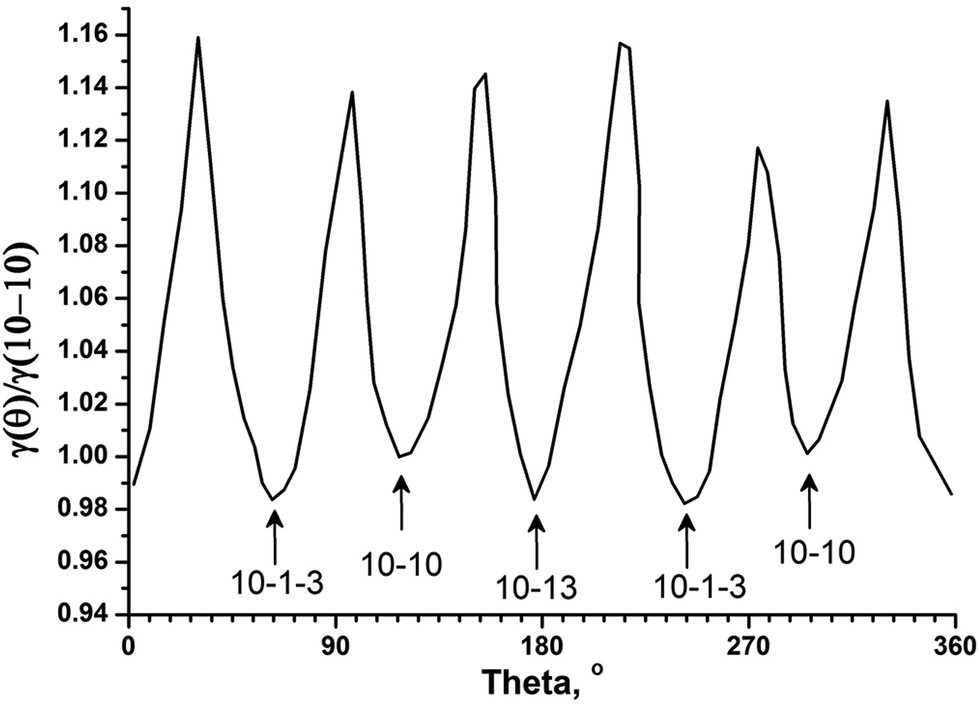 | ||
| Fig. 3 Radius of hole r(i) vs. θ plot extracted from Fig. 2(e). The r(i) axis is normalized with respect to the r value of γ(10−10). | ||
To gain the SE information of the other facets, ZnO nanobelts with the preferred growth direction along [10−10] is attempted. Fig. 4(a) shows the typical ZnO nanobelt with a length of 8.9 μm and width of 0.6 μm. The nanobelt is tilted to the <0002> zone axis prior to irradiation as shown in the inset of Fig. 4(a). The nanobelt was then irradiated with 200 keV electrons (FEI Tecnai T20) for about 80 seconds with a beam current of ≈ 10 pA. Fig. 4(b) shows the hole with a regular hexagonal shape formed after irradiation. It is to be noted that at this zone axis, {10−10} and {11−20} are the most likely facets to be present in a probable equilibrium hole. Both facets have similar SE, which is much less than that of {0002} and {10−11}. Hence an equilibrium hole may be easier to develop under the conditions (as in the case of 200 keV with a beam current of ≈ 10 pA) in which we did not achieve equilibrium holes in the previous case of the nanorods. This implies that facets with higher SE may require more intense conditions (higher beam energy and/or higher beam current) to evolve. Based on the ED pattern, the facets are identified as {10−10}, {−1100} and {01−10}, which are the members of the {10−10} set of planes. Hence all the facets should have the same SE, consistent with the regular hexagon shape. This analysis suggests that the SE of the {11−20} is higher than that of the {10−10} and this method of projection into two dimensions imposes limitations on exploring the SEs of all low index facets.
 | ||
| Fig. 4 (a) TEM image of an as-grown ZnO nanobelt before irradiation with the inset showing the diffraction pattern along the <0002> zone axis. (b) TEM image of a hole in the ZnO nanobelt created upon 200 keV electron beam irradiation. Schematic diagram of the hole with the facets identified as {10−10} shown in the inset. (c) TEM image of holes in a GaN thin film created due to 300 keV electron beam irradiation with the inset showing the schematic diagram of the hole with the facets identified as {10−10} and {10−13}. | ||
Finally, a c-oriented GaN thin film grown on a sapphire substrate is considered. A cross-sectional TEM specimen was prepared for the electron irradiation using a 300 keV transmission electron microscope (FEI TITAN) for about 60 seconds with a beam current of ≈ 7 nA. The sample was tilted to the <2−1−10> zone axis (same as the ZnO nanorod) prior to in situ electron irradiation experiments using TEM. Fig. 4(c) shows the typical result containing two pores and all the holes share the identical shape developed in the ZnO nanorod shown in Fig. 2(d). By running the same procedures, the facets are composed of {10−10} and {10−13}, and the average value of γ(10−13) and γ(10−1−3) for GaN is determined to be ≈1.36 J m−2 if taking γ(10−10) as 1.40 J m−2.9
Hole drilling is influenced by the energy of the electron beam, the thickness along the beam direction and the bonding of constituent atoms with each other, which is related to the surface energy. Hole drilling is caused by several processes: (i) knock-on damage due to an energetic electron beam via momentum transfer (sputtering), (ii) evaporation of atoms due to heat generation caused by an energetic electron beam (sputtering) and (iii) radiolysis through inelastic scattering (ionization plus sputtering). In knock-on damage, target atoms will receive maximum energy (Tm) transferred from the incident electrons and are displaced from their lattice sites permanently if Tm is larger than the displacement energy (Ed). The displacement energy of an atom in a facet is material dependent and directly proportional to its binding energy in that lattice site. Consequently, this energy must be proportional to the SE and inversely proportional to the rate of sputtering (removal of atoms) for a given beam energy. In other words, the lower the SE, the higher the sputtering yield and hence the greater the chance that a new surface is created from hole drilling. In the case of ZnO, Tm for Zn and O is 13 and 55 eV for 300 keV electrons, respectively. In the case of GaN, Tm for Ga and N is 12 and 61 eV for 300 keV electrons, respectively (using the formulae given in ref. 23 summarised in Table 2). Whereas Ed is 65 and 50 eV for Zn and O in ZnO, respectively,24Ed is 73 and 32 eV for Ga and N in GaN,25 respectively. It is evident that for Zn and Ga atoms Tm < Ed and hence atoms can not be removed (sputtering) by only direct momentum transfer even using 300 keV electrons. Irradiation with a beam of energetic collimated electrons can induce a sharp temperature rise in the target which is proportional to the energy and flux of the incident electron beam and density and structure of the target material. For 300 keV electrons with a typical beam current of ≈7 nA, the projected range of electrons in bulk ZnO is ≈85 μm.26 In this case the temperature rise is about 12 K only.23 But the temperature rise could be more in lower dimensional structures compared to 3D due to lower heat dissipation. For example, in the case of a 0D structure (e.g. fullerene), if we consider Tm = 30 eV, then the temperature rise for 0D structures can be approximately calculated as ≈2000 K![[thin space (1/6-em)]](https://www.rsc.org/images/entities/char_2009.gif) 27 which is much higher than that of 3D structures. As the temperature of the target increases, the heat of sublimation decreases and hence the binding energy also decreases.28 This means, with higher target temperature, the sputtering yield is higher29 leading to greater chances of getting holes. Hence, sputtering enhancement i.e. more removal of atoms could be the combined effect of evaporation due to the higher target temperature (due to higher beam energy and/or current) and momentum transfer (due to higher beam energy). The third possibility is that the electron beam first ionises O and N in the ZnO and GaN matrix leaving metallic Zn and Ga behind, respectively. The displacement energy for metallic Zn is about 11 eV30 and 12 eV for Ga.31 These values are comparable to the corresponding Tm and hence sputtering of Zn and Ga atoms via direct knock-on damage subsequently occurs.
27 which is much higher than that of 3D structures. As the temperature of the target increases, the heat of sublimation decreases and hence the binding energy also decreases.28 This means, with higher target temperature, the sputtering yield is higher29 leading to greater chances of getting holes. Hence, sputtering enhancement i.e. more removal of atoms could be the combined effect of evaporation due to the higher target temperature (due to higher beam energy and/or current) and momentum transfer (due to higher beam energy). The third possibility is that the electron beam first ionises O and N in the ZnO and GaN matrix leaving metallic Zn and Ga behind, respectively. The displacement energy for metallic Zn is about 11 eV30 and 12 eV for Ga.31 These values are comparable to the corresponding Tm and hence sputtering of Zn and Ga atoms via direct knock-on damage subsequently occurs.
Although knock-on damage (elastic displacements of target atoms) requires a threshold beam energy, beam current (also flux) plays an equally important role particularly in temperature rise, which may lead to radiolysis for hole drilling when an extremely condensed electron beam is used. Whereas knock-on damage is proportional to the incident energy, the inelastic scattering cross section decreases with the increasing incident energy. Electron beam radiation damage as well as hole drilling on various materials have been studied23,27,32–38 where they concluded that not only elastic scattering but also beam heating and sometimes radiolysis, depending upon the material, caused sputtering. If hole drilling occurs solely via radiolysis, the time taken to drill a hole must be independent of the foil thickness as long as the foil thickness along the beam direction is lower than the projected range of the electron beam.35,39 However, no attempt has been made to extract the SE of the material from the drilled hole. Holes formed in these reported studies were present with irregular shapes (e.g. see ref. 35) resulting from off-zone axis electron irradiation, whereas this issue is taken with care in this report as SE derivation demands zone-axis electron irradiation. In our case, the maximum transferred energy (Tm) of atoms both in ZnO and GaN are less than the displacement energy (Ed) of the same. The sputtering responsible for hole drilling must be a combined effect of beam energy and beam current (temperature rise due to beam heating effect).
It is important to note that, this procedure to derive SE is limited by certain factors. In order to get an equilibrium hole, the self-supported nanostructures must be tilted to a higher symmetric zone axis and facets could be anticipated from the respective diffraction pattern. As the electron irradiation is carried out inside a transmission electron microscope, the procedure is limited by the tilt range of the instrument to go from one zone axis to another for the same nanostructure. This could be overcome to some extent by choosing nanostructures with different growth directions (as in the case of the ZnO nanobelt with growth direction [10−10]), hence different equilibrium holes. Similarly one can explore all the possible equilibrium holes with the choice of orientations and materials of nanostructures. In principle one can derive the SEs of all possible facets of any material if exposed, provided that at least one facet is known (either from theory or experiment).
4. Conclusions
The surface free energy of different facets of ZnO and GaN has been derived only using in situ transmission electron microscopy. Inverse Wulff's construction has been applied to the holes drilled by an electron beam available with TEM. This may be extended to almost any material to find the SE of any facet, provided the required tilt is possible for the nanostructure. To prove its versatility and capability, a ZnO nanorod (1D), a ZnO nanobelt (2D) and a GaN thin film (3D) were used as examples. This is a unique utilization of TEM which definitely opens up an important fundamental research area.Acknowledgements
The authors acknowledge the Center for Micro/Nano Science and Technology, NCKU for equipment access and technical support. J. Ghatak sincerely acknowledges Prof. C. N. R. Rao for providing an advanced microscopy facility for this research and Dr Ranjan Datta at ICMS, JNCASR for providing the GaN thin film sample grown at Cambridge GaN Center, University of Cambridge, UK.References
- W. R. Tyson, Surf. Sci., 1977, 62, 267–276 CrossRef CAS.
- H. Jones, Met. Sci., 1971, 5, 15–18 CrossRef CAS.
- R. J. Jaccodine, J. Electrochem. Soc., 1963, 110, 524–527 CrossRef CAS.
- C. Messmer and J. C. Bilello, J. Appl. Phys., 1981, 52, 4623–4629 CrossRef CAS.
- A. Wander and N. M. Harrison, Surf. Sci., 2000, 468, L851–L855 CrossRef CAS.
- B. Meyer and D. Marx, Phys. Rev. B: Condens. Matter, 2003, 67, 035403 CrossRef and therein.
- M. Kim, Y. J. Hong, J. Yoo, G. Yi, G. Park, K. Kong and H. Chang, Phys. State Solidi RRL, 2008, 2, 197–199 CrossRef CAS.
- S. Na and C. Park, J. Korean Phys. Soc., 2009, 54, 867–872 CrossRef CAS.
- Y. J. Hong, J. Yoo, Y. Doh, S. H. Kang, K. Kong, M. Kim, D. R. Lee, K. H. Oh and G. Yi, J. Mater. Chem., 2009, 19, 941–947 RSC.
- J. I. Sohn, et al. , Sci. Rep., 2014, 4, 5680 CAS.
- J. E. Northrup and J. Neugebauer, Phys. Rev. B: Condens. Matter, 1996, 53, R10477–R10480 CrossRef CAS.
- T. W. Kim, Y. J. Hong, G. Yi, J. Kwon, M. Kim, H. N. Han, D. H. Kim, K. H. Oh, K. Kong and Y. Kwon, J. Phys. D: appl. Phys., 2008, 41, 015406 CrossRef.
- G. Wulff, Z. Kristallogr. Mineral., 1901, 34, 449 CAS.
- C. Herring, Phys. Rev., 1951, 82, 87 CrossRef CAS.
- D. J. Eaglesham, A. E. White, L. C. Feldman, N. Moriya and D. C. Johnson, Phys. Rev. Lett., 1993, 70, 1643–1646 CrossRef CAS PubMed.
- D. M. Follstaedt, Appl. Phys. Lett., 1993, 62, 1116–1118 CrossRef CAS.
- J. Ghatak, J. Huang, P. Huang, Y. Shih and C. P. Liu, J. Electrochem. Soc., 2012, 159(3), H239–H242 CrossRef CAS.
- N. D. Browning, M. F. Chisholm and S. J. Pennycook, Nature, 1993, 366, 143–146 CrossRef CAS.
- M. Varela, A. R. Lupini, H. M. Chrwisten, A. Y. Borisevich, S. J. Pennycook, N. Dellby, O. J. Krivanek, P. D. Nellist, S. D. Findlay, M. P. Oxley and L. J. Allen, Phys. Rev. Lett., 2004, 92, 095502–095505 CrossRef CAS PubMed.
- P. Schattschneider, S. Rubino, C. Hebert, J. Rusz, J. Kunes, P. Novák, E. Carlino, M. Fabrizioli, G. Panaccione and G. Rossi, Nature, 2006, 441, 486–488 CrossRef CAS PubMed.
- D. A. Muller, T. Sorsch, S. Moccio, F. H. Baumann, K. Evans-Lutterodt and G. Timp, Nature, 1999, 399, 758 CrossRef CAS; D. A. Muller, Y. Tzou, R. Raj and J. Silcox, Nature, 1993, 366, 725–727 CrossRef.
- R. Datta and C. J. Humphreys, Phys. State Solidi (c), 2006, 3, 1750–1753 CrossRef CAS.
- R. F. Egerton, P. Li and M. Malac, Micron, 2004, 35, 399–409 CrossRef CAS PubMed.
- K. Lorenz, E. Alves, E. Wendler, O. Bilani, W. Wesch and M. Haye, Appl. Phys. Lett., 2005, 87, 191904 CrossRef.
- H. Y. Xiao, F. Gao, X. T. Zu and W. J. Weber, J. Appl. Phys., 2009, 105, 123527 CrossRef.
- Monte Carlo Simulation of electron Trajectory in Solids, http://www.gel.usherbrooke.ca/casino/.
- A. V. Krasheninnikov and K. Nordlund, J. Appl. Phys., 2010, 107, 071301 CrossRef.
- S. J. Zinkle and C. Kinoshita, J. Nucl. Mater., 1997, 251, 200–215 CrossRef CAS.
- J. Ghatak, B. Sundaravel, K. G. M. Nair and P. V. Satyam, J. Phys. D: Appl. Phys., 2008, 41, 165302 CrossRef.
- A. S. A. Karim, M. E. Whitehead, M. H. Loretto and R. E. Smallman, Acta Metall., 1978, 26, 975–981 CrossRef CAS.
- S. Myhra and R. B. Gardiner, Radiat. Eff., 1975, 27, 35 CrossRef CAS.
- I. G. Salisbury1, R. S. Timsit1, S. D. Berger1 and C. J. Humphreys1, Appl. Phys. Lett., 1984, 45, 1289–1291 CrossRef.
- P. S. Turner, T. J. Bullough, R. W. Devenish, D. M. Maher and C. J. Humphreys, Philos. Mag. Lett., 1990, 61, 181–193 CrossRef CAS.
- S. Bysakh, M. Shimojo, K. Mitsuishi and K. Furuya, J. Vac. Sci. Technol., B, 2004, 22, 2620–2627 CAS.
- D. G. Howitt, S. J. Chen, B. C. Gierhart, R. L. Smith and S. D. Collins, J. Appl. Phys., 2008, 103, 024310 CrossRef.
- R. F. Egerton, R. McLeod, F. Wang and M. Malac, Ultramicroscopy, 2010, 110, 991–997 CrossRef CAS.
- J. Ghatak, W. Guan and G. Möbus, Nanoscale, 2012, 4, 1754–1759 RSC.
- J. Shim, J. A. Rivera and R. Bashir, Nanoscale, 2013, 5, 10887–10893 RSC.
- R. M. Allen, S. J. Lloyd and C. J. Humphreys, Inst. Phys. Conf. Ser., 1997, 138, 87–90 Search PubMed.
Footnote |
| † Electronic supplementary information (ESI) available. See DOI: 10.1039/c5nr06198a |
| This journal is © The Royal Society of Chemistry 2016 |