
Charging C60 islands with the AFM tip†
Brice
Hoff
,
Claude R.
Henry
and
Clemens
Barth
*
CNRS, Aix-Marseille University, CINaM UMR 7325, Campus de Luminy, Case 913, 13288 Marseille Cedex 09, France. E-mail: barth@cinam.univ-mrs.fr; Fax: +33 (0)4 91 41 89 16; Tel: +33 (0)6 60 36 28 19
First published on 12th November 2015
Abstract
We show that electrons can be transferred on demand from an AFM tip into single bulk-like C60 islands, which are supported on the insulating NaCl(001) surface. We exemplify this by controlled charge-manipulation experiments conducted in ultrahigh vacuum by noncontact AFM (nc-AFM), electrostatic force microscopy (EFM) and Kelvin probe force microscopy (KPFM). KPFM shows a homogeneous contrast at the islands, which is a signature for an equal distribution of the electrons in the T1u band. The charge dissipates during half a day due to an interaction of the charged C60 islands with defects in the near surface region of NaCl. Our results open the perspective in photo-voltaics to study charge attachment, stability and charge exchange with the environment of any C60 bulk-like system.
1. Introduction
Since their experimental discovery in 1985,1 buckminsterfullerenes (C60) have been a subject for many investigations2 like in superconductivity,3 biochemistry4 and in particular in the domain of photo-voltaics, where fullerenes and derivatives are used in two-dimensional organic thin films.5 Based on weak van der Waals forces, C60 molecules crystallize at room temperature into a solid with a fcc lattice,6,7 which has fascinated research ever since as exemplified by a large amount of scanning tunneling microscopy (STM) work on thin C60 films.8 STM gives great insights into phenomena of self-assembly,9,10 and even the orientation of single C60 molecules can be studied with high precision.11 The molecules have also been imaged by noncontact atomic force microscopy in particular on insulating surfaces.12–17 As shown by the revolutionary nc-AFM work of the Meyer group,18 the inner atomic structure of a C60 molecule can be resolved at low temperatures,19 with an unmatched precision in comparison with STM.20A fascinating property of the single C60 molecule is that due to its large electron affinity of EAmol = 2.6 eV and low activation energy for electron attachment the molecule is a good electron acceptor:21–23 a free C60 molecule can accept several electrons with the single anion C60− being relatively stable.24,25 With respect to bulk C60, calculations exhibit a semi-conducting character of the solid due to the Hu band being completely filled with electrons and the empty T1u band, both separated by a band gap of about Egap∼ 2.6 eV.26 The electron affinity increases when C60 is in bulk form reaching a value of EAbulk∼ 3.6 eV.27,28 When in particular thin films of C60 are grown on metal surfaces an intrinsic charge transfer between the metal and the film takes place,29 as exemplified by the work of Modesti and collaborators:30 a growth of C60 islands on Au(110)c2 × 2 leads to a charge transfer of 2 electrons per molecule at the interface. Even more, in the presence of a mono-layer (ML) of potassium on the same gold surface the amount of transferred charge raises to 3 electrons per molecule, with the largest charge transfer of 6 electrons per molecule when the film is supported on a very thick potassium film. Such experiments could be enriched by the observation that alkali atoms can be intercalated in the C60 solid,31,32 as demonstrated by STM experiments in the Crommie group on K/C60 films supported on Au(111):33,34 electrons are transferred from potassium to the C60 molecules and when increasing the amount of potassium from K3C60 to K4C60 the C60 film changes its electronic configuration from insulating to metallic.
In the past, the direct capture of electrons by single C60 molecules was realized by crossing an electron beam with a molecular beam of C60, which yielded important information about, e.g., the lifetime of single C60 anions.25 The curious question is, whether electrons can also be explicitly transferred into supported, bulk-like C60 islands without any intrinsic charge transfer between the islands and the surface or dopants (adsorbed or intercalated atomic species). In other words, can we charge C60 islands in a direct manner with electrons, for instance with the help of an AFM tip? Such type of direct charging would open the perspective to study charge attachment, stability and also charge transport in the C60 bulk system, which is of particular importance for applications in, e.g., photo-voltaics.
In this paper, we show that electrons can be indeed transferred on demand from the AFM tip into single bulk-like C60 islands. We exemplify this by controlled charge-manipulation experiments conducted by noncontact AFM (nc-AFM), electrostatic force microscopy (EFM) and Kelvin probe force microscopy (KPFM) in ultrahigh vacuum. Elementary surface charges could have been detected in the past by EFM35,36 and KPFM37,38 with nanometer resolution, and elementary charges have also been explicitly injected from the tip to the surface.39,40 We conducted experiments on the (001) surface of a thick insulating bulk NaCl crystal because NaCl(001) has a large band gap of 8.5 eV (ref. 41) so that a priori no immediate intrinsic charge transfer can be expected between C60 islands and NaCl(001). We describe the charging of single C60 islands, the characteristics of charged C60 islands and time dependent charge dissipation processes, which appear within half a day due to an interaction between charged C60 islands and the NaCl(001) support.
2. Experimental section
The preparation of the NaCl(001) surface, the deposition of the C60 molecules and the AFM experiments are conducted in one UHV chamber. Technical details of the sample preparation, nc-AFM and the two electrostatic imaging modes can be found in the ESI.† In the following we summarize the most important aspects of the experimental methods.Frequency modulated noncontact AFM (nc-AFM) experiments are conducted with a room temperature AFM/STM system in a UHV chamber maintaining a base pressure in the low 10−10 mbar range. Conducting silicon cantilevers with a resonance frequency of 280 kHz are used, with oscillation amplitudes stabilized at some nanometers.
We use frequency modulated Kelvin probe force microscopy (FM-KPFM)37,42 and electrostatic force microscopy (FM-EFM)35,36 where a DC (Udc) and AC voltage (Uac = 1.5 V) with frequency fac = 475 Hz are applied to the sample during the nc-AFM topography imaging mode (tip is grounded). In KPFM, the DC bias voltage is varied by a Kelvin feedback loop such that the electrostatic tip–surface interaction is minimized at each point on the surface. The minimizing Kelvin voltage equals then the apparent contact potential difference U between the metallic sample holder and the tip in the presence of the NaCl insulator.43 Thanks to the modulation technique, a second, so-called Kelvin image representing the Kelvin voltage at each pixel is obtained in the standard topography imaging mode. In our set-up, a bright contrast in Kelvin images corresponds to more positive Kelvin voltages and vice versa. When we image the surface in the EFM mode, we de-activate the Kelvin regulator, apply a constant DC voltage (Udc), extract the amplitude of the detuning signal (Δf) at the frequency fac and record this amplitude in a separate image.35,36 The distribution of surface charges is represented by EFM35,36 and KPFM37,38 images.
Millimeter thick NaCl single crystals of highest purity (size: 4 × 4 × 10 mm2) are outgassed by annealing at ∼200 °C in an oven, which is located inside the UHV chamber.44 After cooling of a crystal and its sample holder, a clean (001) surface is obtained by in situ cleavage of the crystal along the (001) plane at room temperature. The crystal is then annealed again in UHV at around ∼200 °C for a few hours to put the crystal into its equilibrium charge state, as described in ref. 38. The C60 molecules are evaporated at 330 °C from a Knudsen cell onto the substrate kept at room temperature, with a deposition rate of 0.3 ML min−1.
3. Results
After the preparation of a clean NaCl(001) surface by UHV cleavage and following annealing of the NaCl crystal in UHV, a few hundreds of nanometer wide, atomically flat terraces and one ML high steps with a typical density of 108 to 109 steps per cm2 are obtained on NaCl(001). Depositing 0.5 ML C60 onto such a surface leads to typical characteristics of C60 islands [Fig. 1], which have been previously described:13 due to the weak substrate–molecule interaction and the high mobility of the molecules, the islands grow at the NaCl steps in a Volmer–Weber growth mode, leading to three-dimensional C60 islands with (111) top facets [Fig. 1(a)]. The islands have a lateral extension of up to 150 nm and are always completed by two molecular layers, with the following uncompleted layers on the third and fourth molecular height levels [Fig. 1(b) and (c)].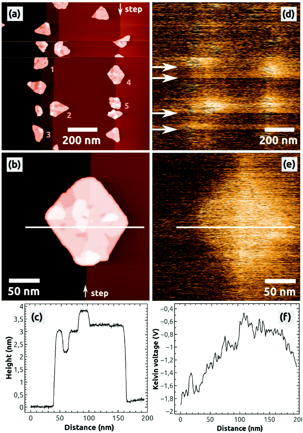 | ||
| Fig. 1 nc-AFM topography (a, b) and Kelvin images (d, e) of C60 islands grown at one ML high steps on the NaCl(001) surface. Images (a, d) and (b, e) were obtained each within one KPFM measurement. The height profile (c) taken from the topography image (b) exemplifies that an island can be built by up to 4 ML. The Kelvin image (d) shows that during the imaging the islands can get charged by the AFM tip, which is visible by the contrast changes (bright) marked by the arrows (see also profile (f)). The Kelvin image (e) shows that upon charging a C60 island a uniform bright contrast with respect to NaCl(001) is observed. Image sizes: 1 × 1 μm2 (a, d), 240 × 240 nm2 (b, e), speed: 0.5 Hz, Δf = −21.8 Hz. | ||
To analyze the charge state of such islands, we always conducted KPFM measurements because respective Kelvin images represent the distribution of surface charges.37,38 We consider the NaCl(001) terraces to be defect-free and charge-neutral (see section 4) so that they always serve as a reference for KPFM measurements, expressed by the Kelvin voltage UNaCl.
In general, we do not observe a preferred Kelvin contrast between the C60 islands and the stoichiometric NaCl(001) terraces (ΔUC60–NaCl = UC60 − UNaCl), which might be due to the typically relative high noise of some hundreds of mV in the Kelvin voltage where possible small contrast differences are hidden. However, during the imaging we occasionally observe changes of the Kelvin contrast as shown in Fig. 1(d): in the scanning lines marked by the four arrows the mean Kelvin contrast changes to a bright contrast, producing three bright bands. Such changes of the mean Kelvin voltage were observed and characterized before45 and can be unambiguously assigned to changes of the electrostatic configuration of the tip apex. Because of the brighter Kelvin contrast, which corresponds to a more positive mean Kelvin voltage, we can conclude that the tip apex obviously got more positive.45 Interestingly, such changes of the electrostatic tip configuration were not necessarily accompanied by tip-changes visible in the topography image [compare Fig. 1(d) with Fig. 1(a)]. Furthermore, the tip was stable only within a few scanning lines (bright bands) but switched back after a relatively short time to its initial electrostatic configuration (dark bands).
A very important second observation is that within the bright bands a bright Kelvin contrast between the five C60 islands (1 to 5) and the stoichiometric NaCl(001) terraces can be observed [Fig. 1(d)]. In the following measurements, only the islands 1 to 5 appeared with a homogeneous bright contrast, as exemplified for one island by the image in Fig. 1(e): a typical homogeneously distributed bright contrast can be found, corresponding to a Kelvin voltage difference of ΔUC60–NaCl ≈ +1 V with respect to NaCl(001) [Fig. 1(f)].
As discussed further below, the latter contrast phenomena in Fig. 1(d) can be assigned to a charging of the C60 islands by the tip. With respect to the Kelvin contrast formation of surface charges that have been discussed before,38 the islands obviously contained negative charges because a more positive Kelvin voltage was applied at the islands (bright contrast) with respect to the neutral NaCl(001) terraces (dark contrast).
To study charges in C60 islands in more detail we conducted controlled charge manipulation experiments, which are documented in Fig. 2. They were done on the same sample surface after the measurements shown in Fig. 1. We decided to charge the islands during the imaging in the EFM mode and by increasing the sample bias voltage to positive values such that negative charge from the tip is attracted towards the C60 islands. The topography image from a KPFM measurement in Fig. 2(a) shows two selected, uncharged C60 islands, which are composed of 3 to 4 molecular layers [see the profile in Fig. 2(b)]. The image in Fig. 2(c) of the same islands was obtained in the EFM mode at a bias voltage of UBias = +2.0 V, which was far beyond the Kelvin voltage of about −1 V needed to minimize the electrostatic tip–surface interaction above NaCl(001) and the islands. This means that the image in Fig. 2(c) and the following EFM images [Fig. 2(e), (g) and (h)] were acquired with a relatively strong electrostatic field between the tip and the island. This explains the dark contrast of the islands with respect to NaCl(001), which probably is a result of the much smaller polarization of NaCl (α ≈ 0.16 Å3 (Na+) and 3.1 Å3 (Cl−)46,47) with respect to C60 (α ≈ 76 Å3 (ref. 48)) in the presence of the strong electrostatic field.
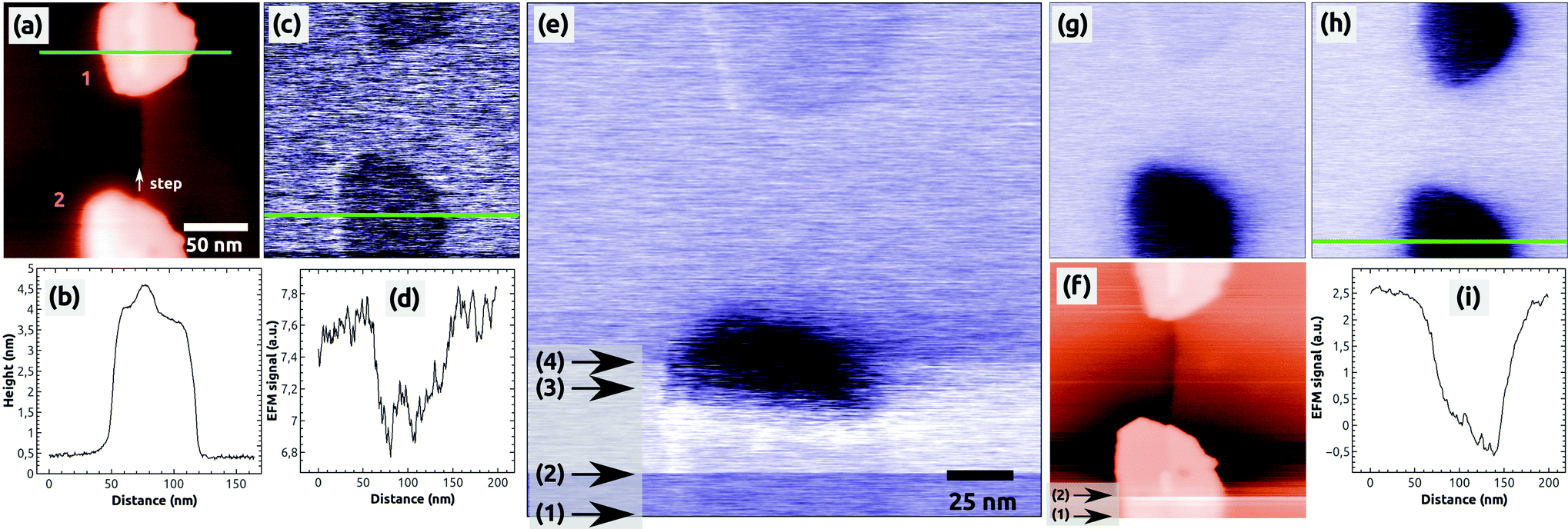 | ||
| Fig. 2 The controlled charging of two C60 islands by the AFM tip. Both islands are located at a one ML high step of NaCl. (a) Topography image of the two islands (1 and 2), with the corresponding height profile (b). (c) EFM image of the uncharged islands, both of which exhibit a faint dark EFM contrast as shown in the profile (d). (e) EFM image obtained during the charging of island 1 with the corresponding topography image (f). (g) EFM image after the charging of island 1. (h) EFM image of the two islands after a second controlled charging of the island 2. The profile (i) shows the strong EFM contrast of island 2. Image sizes: 200 × 200 nm2, speed: 0.5 Hz, Δf = −7.4 (a), −11.8 (c), −14.0 (mean value) (e, f), −13.8 (g) and −15.8 Hz (h), EFM bias voltage: +2.0 V (c), (g) and (h), for image (e) see the text. | ||
The following EFM measurement [Fig. 2(e)] was obtained by scanning the surface from the bottom to the top. We first imaged the bottom island with a bias voltage of UBias = +2.0 V and increased slowly the voltage by a few hundreds of mV in the region marked by the arrows 1 and 2. When regulating the tip–surface distance on a constant detuning value given by Δf = Δfvan der Waals + Δfel = const (constant Δf mode), an increase of the bias voltage leads to an increase of the electrostatic contribution (Δfel) and at the same time a decrease of the van der Waals contribution (Δfvan der Waals), which is responsible for the topography contrast. The result is that the tip is retracted from the surface leading to a fluffy topography contrast as it can be seen in the region marked by the two arrows in Fig. 2(f).
Therefore, in the scanning line at arrow 2 [Fig. 2(e)], we decreased the pre-set value of Δf = −14 Hz to the more negative value of −16 Hz (tip approach) to get back the initial sharp topography contrast of the island. In the region marked by arrows 2 and 3, the bias voltage was further increased until we reached a value of UBias = +2.5 V (arrow 3), at which within a few scanning lines a sudden strong contrast change appeared at the island: the island changed its faint dark contrast to a very dark one. Immediately after this change the bias voltage was monotonously decreased within a few scanning lines onto its initial value of UBias = +2.0 V, and at the same time, the pre-set value of Δf was accordingly increased from −16 Hz to −12 Hz (tip retraction). No further changes of the bias voltage and detuning were done afterwards. In the last part of the image (from arrow 4 onwards) the top island still appears in its faint initial dark contrast.
The change of contrast of the bottom island can be well seen in the following EFM image [Fig. 2(g)], which was acquired with a bias voltage of UBias = +2.0 V and without any other changes of the scanning parameters: the bottom island appears in a dark contrast whereas the top island appears in its initial, faint dark contrast. This is a clear signature that the bottom island was charged by the tip (see also below) whereas the top island remained uncharged. Note that we did not observe any changes of the island morphology – the island exhibited same geometric properties in the topography images before and after the charging (see ESI Fig. S1†). Note furthermore that the damping image shows a preferred contrast at the bottom island, which is discussed in the ESI (Fig. S1 and S2†).
In a second, independent charging experiment, we could charge the top island with the AFM tip by following the same charging protocol described above, i.e., by applying exactly the same bias voltage of UBias = +2.5 V. The image in Fig. 2(h) shows both islands in a strong dark contrast after the second charging [see the profile in Fig. 2(i)]. After this EFM measurement, we switched to the KPFM imaging mode and obtained the Kelvin image shown in Fig. 3(a). A large contrast difference between the two C60 islands and the NaCl(001) terraces of up to ΔUC60–NaCl = +7 V can be seen in the profile Fig. 3(b). Such values are a strong signature that negative charges were transferred from the tip into the islands (see ref. 38 for contrast interpretation). Another clear signature for the controlled charge transfer can be found in the images of Fig. 4(a) and (b), which show the same region of the surface on a larger scale (zoom out) with the charged islands located in the middle of the image at positions 1 and 2, and other C60 islands in the vicinity (e.g., at 3 and 4): the islands in the vicinity do not exhibit any Kelvin contrast with respect to NaCl(001), which means that they were not charged during the two charging experiments. Note that the two charged islands, 1 and 2, appear in a bright Kelvin contrast gradually increasing from the left to the right, which is discussed in the ESI.†
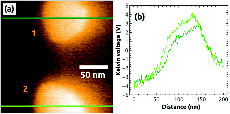 | ||
| Fig. 3 A Kelvin image (a) simultaneously obtained during the acquisition of Fig. 2(a), 2 hours after the charging of the second island 1. The profiles were taken at the green lines in image (a). Image size: 200 × 200 nm2, speed: 0.5 Hz, Δf = −7.4 Hz. | ||
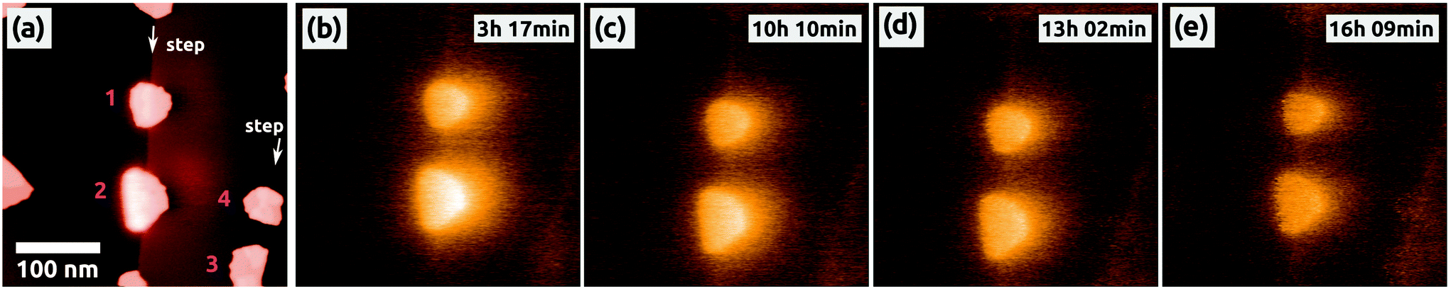 | ||
| Fig. 4 The decrease of the charge inside the two C60 islands (1 and 2), which have been charged before by the AFM tip [see Fig. 2]. All islands are located at one ML high steps of NaCl. (a) Topography and simultaneously obtained Kelvin image (b) showing also other C60 islands in the vicinity of the two charged islands, e.g., at 3 and 4. (c)–(e) Selected Kelvin images, which were obtained consecutively without changing any scanning parameters. The corresponding topography images of the latter Kelvin images are not shown. All Kelvin images have the same color scale, which ranges from −1.2 V (dark, NaCl) to +8.0 V (bright). The time is the one passed by after the charging of the second island (1). Image sizes: 500 × 500 nm2, speed: 0.5 Hz, Δf = −6.8 Hz. | ||
To our surprise, we could make an interesting observation: about 3 h after the second charging of the top island (1) we recorded 25 measurements of the two islands within 13 hours, during which we did not change any parameters of the scanning. Fig. 4(a) and (b) are the second measurement of the series, and the following selected Kelvin images from the series are shown in Fig. 4(c)–(e). All Kelvin images have the same color scale, with the reference contrast of the NaCl(001) terraces represented in one and the same color. As it can be seen, the brightness of the two charged islands decreased by time, which means that the Kelvin voltage difference between the charged islands and the NaCl(001) terraces, ΔUC60–NaCl = UC60 − UNaCl, decreased from image to image. We clearly exclude a possible discharge induced by the tip because we did not observe in any of the images the typical signatures discussed for the occasional charging of islands during the scanning [Fig. 1(d)], which we expect to appear also during a discharging.
The voltage difference ΔUC60–NaCl for the two islands, (1) and (2), is shown as a function of time in Fig. 5a. Starting from a high value of ΔUC60–NaCl ≈ +6.5 V the voltage difference decreased faster for island 2 than for island 1 (from ΔUC60–NaCl ≈ +5.4 V), whereas after about 13 hours both decreased onto a similar level of ΔUC60–NaCl ≈ +3.5 V. Some fluctuations can be seen, which are, however, within the error bar of the values, which we extracted from the Kelvin images. No decrease in a staircase shape can be seen, which would otherwise point to a charge removal of single electrons as observed on Si3Ni4 thin films.49
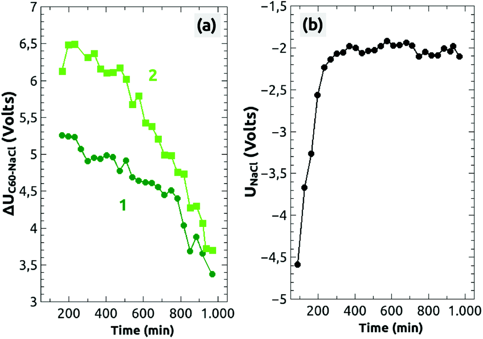 | ||
| Fig. 5 (a) The time dependent decrease of the charge inside the two C60 islands (island 1: dark green, island 2: green). (b) Time dependent charge phenomena that appeared probably in the tip. In the left graph (a) the difference of the Kelvin voltages between the charged C60 islands and NaCl, ΔUC60–NaCl = UC60 − UNaCl, is shown whereas the right graph (b) shows the Kelvin voltage between the tip and the sample above the NaCl(001) surface (UNaCl). | ||
On the same time scale, the Kelvin reference voltage recorded above the NaCl(001) terrace (UNaCl) shows an interesting course [Fig. 5(b)]: the voltage was first at UNaCl ≈ −4.6 V but increased after 3 hours onto a rather constant value of around UNaCl ≈ −2 V. As stated above, we consider the NaCl(001) terraces to be charge-neutral, on which no charge phenomena take place. Therefore, the increase can only be due to a slow movement of charged defect-like vacancies or dislocations below the surface50 or more likely due to slow changes of the electronic tip configuration.
4. Discussion
4.1 Charging mechanism and condition
The experiments documented in Fig. 2 show that in general, C60 islands can be explicitly charged with electrons on demand by the AFM tip. From the bright Kelvin contrast at the two islands in Fig. 3 and 4 it can be concluded that electrons were transferred from the tip to the islands, which is certainly highly facilitated by the high electron affinity of bulk C60. The electronic structure of bulk C60, if neutral, has a semi-conducting nature26 with the Hu band being completely filled with electrons and an empty T1u band. We believe that transferred electrons are then located in the latter conduction band. Obviously, the electrons are equally distributed over the entire islands and not localized at some local positions at the islands.The direction of the charge transfer is in agreement with the applied positive voltage of +2.5 V, which was more positive with respect to the minimizing Kelvin voltage of ∼−1 V: electrons in the tip are attracted towards the positive sample holder, which carries the NaCl crystal and at which the bias voltage was applied to. With respect to the tip–surface distance, we observed a relatively sharp topography contrast of the islands, which indicates that the tip had a distance of below 2 nm to the islands. Therefore, we strongly anticipate that a tunneling of electrons from the tip towards the islands appeared because of the above mentioned potential difference between the tip and the C60 islands and the small tip–C60 distance, which both increase the tunneling probability as discussed before.40,51
We clearly stress that the charging voltage of +2.5 V found here may vary from experiment to experiment and in particular is dependent on the tip. We discuss this with the help of the energy diagram shown in Fig. 6, in which we consider an idealized surface and tip for simplicity reasons: the NaCl(001) surface and also the representative semi-conducting Si and insulating SiO2 tip have no defect states in their respective band gaps. The conduction and valence bands of the C60 islands are located in the middle of the band gap of NaCl(001) due to the very large band gap of NaCl(001) and the high EA of bulk C60. In this case, we can assume a vacuum alignment of the energy levels as shown in Fig. 6(a). If we now consider an active KPFM experiment, the electrostatic tip–surface interaction is minimized so that the vacuum levels of the tip and the surface are aligned.43 As shown by the three representative tips in Fig. 6(a) (metallic, Si and SiO2 tip), no electrons can be transferred into the T1u band in principle. However, when applying a more positive bias voltage (KPFM switched off) with respect to the Kelvin voltage, electrons can be transferred from the tip to the islands. This applies in particular to metal tips with a relatively low work function (WF), where a voltage below roughly +1.5 V is sufficient. For a Si tip, a larger bias voltage of about +2.5 V at the sample is needed to raise the conduction band of Si such that electrons can tunnel into C60 [Fig. 6(b)]. In the case of an idealized SiO2 tip, a tunneling is almost impossible because very large voltages are needed due to the very large band gap of 9 eV [Fig. 6(a)].
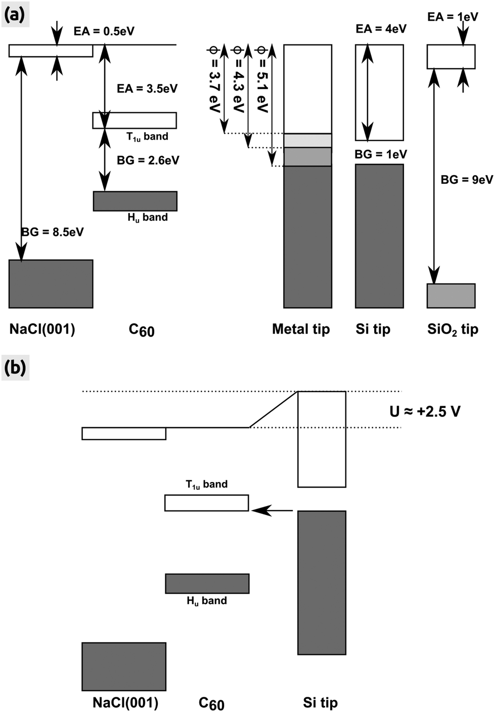 | ||
| Fig. 6 Energy levels of the NaCl(001) surface, bulk C60 island and the AFM tip. (a) All energies after a vacuum alignment. Three different tips (metal, semi-conducting Si and insulating SiO2) are shown whereas the metal tip is represented by three different WFs (ϕ = 3.7, 4.3 and 5.1 eV) symbolizing the WF of polycrystalline magnesium, silver and gold.52 Values for the EA and band gap (BG) were taken from the literature (NaCl(001),41 bulk C60: BG26 and EA27,28). For the Hu and T1u bands we have taken a width of 0.9 and 0.7 eV.53 (b) Energy levels after biasing the sample with a positive voltage of +2.5 V. Electrons can tunnel from the conduction band of the Si tip into C60 (arrow). All energy levels are true to scale. | ||
The above considerations are certainly too simplified because the composition and atomic structure of the foremost part of the tip can strongly deviate from idealized Si or SiO2. For instance, although Si tips exposed to the ambient air carry a native oxide they are probably also hydroxilized and have defect states in the band gap which may potentially contribute to the charging. Furthermore, in typical standard room temperature experiments on NaCl(001), the tip can get contaminated by NaCl from the surface whenever the tip contacts the surface (tip changes). If a small quantity of NaCl in the form of, e.g., a thin film is supported it may strongly influence, e.g., the work function of a conducting support underneath as shown for metal surfaces.54
A very important question is how the electrons tunneled from the tip into the C60 islands during the controlled charging experiments in Fig. 2, and how many electrons were transferred from the tip into the islands. In principle, Fig. 2(e) contains all information about the charging, in particular in the few scanning lines where the island 2 changed its contrast to a dark one. At these positions we could not find any signatures like an expected staircase-like transfer of single electrons from the tip to the C60 island,49 which was probably due to the limited time resolution of the EFM signal. An estimation of the number of transferred electrons is therefore not possible. Electrostatic force spectroscopy as recently done55 can help in future to observe a single electron tunneling and to count explicitly the transferred electrons. Another solution is to explicitly model the geometry composed of the NaCl(001) surface, the C60 island and the tip and in turn calculate the electrostatic tip–surface interaction. However, such a calculation requires a precise knowledge of several parameters like the tip structure and composition, the tip–surface distance and the influence of the thick dielectric NaCl crystal, which are all unknown here.
4.2 Island discharge
With respect to the discharge of the C60 islands [Fig. 4 and 5], we can state that a discharge by the tip during imaging can be ruled out because we did not observe typical charging phenomena as documented in Fig. 1(d), which we otherwise expect to appear also during a discharging of the islands. After a charging, we never observed a topographic change of the islands – and the islands always exhibited same geometric properties in the topography images (see ESI, Fig. S1†). This is why we exclude a possible adsorption of gas molecules from the residual gas of the UHV that could possibly reduce the charge.The most reasonable explanation for the decrease of the island charge is based on the interaction of the charged C60 islands with the NaCl(001) support and more precisely, on the defect environment in the subsurface NaCl region below the islands. In principle, large defect structures such as grain boundaries or dislocations ending on the NaCl(001) surface50 offer possible pathways for the escape of charges.56–58 Such defects could be possibly covered by the C60 islands. However, we never observed grain boundaries or screw dislocations on clean (001) surfaces of our high-quality NaCl single crystals, which would have otherwise produced a clear visible contrast in topography images. For detecting {011}[1![[1 with combining macron]](https://www.rsc.org/images/entities/char_0031_0304.gif) 0] edge dislocations,50 which have their
0] edge dislocations,50 which have their  large Burgers vector in the (001) plane, either atomic resolution can be used or even KPFM59 since such dislocations are charged.50 However, we never observed a Kelvin contrast on, e.g., the flat terraces which can be attributed to charged edge dislocations.
The only explanation that remains is based on the Debye–Frenkel layer,60–62 which was experimentally evidenced by KPFM.38 A Debye–Frenkel layer is composed of positive cation vacancies (VNa+) at kink and corner sites on the surface and a space charge layer below the surface formed by divalent cation impurities like Ca2+, which are contained in any NaCl crystal of even highest purity. In principle, anion vacancies (VCl−) also contribute to the positive space charge layer because anion vacancies exist in any alkali halide even at room temperature. Both charge layers form a surface dipole, which modifies the free formation energies for cation and anion vacancies. In the presence of a charged C60 island this surface dipole is certainly modified such that in particular the positive anion vacancies diffuse to the negatively charged islands. The diffusion is probably also influenced by an electrostatic force gradient originating from the particular geometric shape of the C60 island. If so, it could be that the charge inside the islands is transferred to the positive species. In particular, anion vacancies, which are then transformed into F0 centers, similar to the case described for MgO,63 have a large electron affinity with a high probability to take a charge from the island,64 as it is the case for anion vacancies on MgO(001).65,66
5. Conclusion
We have shown that controlled charge manipulation experiments can be accomplished in UHV at single C60 islands with the help of an AFM tip: the islands can be charged in the frequency modulated EFM mode during nc-AFM imaging by changing the bias voltage continuously to positive voltages. In our experiments we found a charging voltage of +2.5 V, which may, however, vary as a function of the electronic and structural configuration of the tip–surface system. Kelvin images show that electrons are transferred from the tip into the C60 islands and that the electrons are equally distributed inside the islands being responsible for the almost uniform Kelvin contrast of the C60 islands. The charge inside the islands decreases by time on a time scale of half a day inside the UHV, which is due to an interaction of the charged C60 islands with the NaCl support. A possible mechanism for this is based on anion vacancies below the surface that get filled with electrons (creation of F0 centers) at the interface NaCl–C60.Our results form a firm start in the controlled charge manipulation of bulk-like C60 islands on insulating surfaces, with many perspectives included. For instance, we believe that by low-temperature nc-AFM and electrostatic force spectroscopy55 with functionalized metallic AFM tips C60 islands can be charged by single electron charging, which allows counting the transferred charge.
Conducting charge experiments in general helps to determine the electronic structure of charged C60 islands, to give answers to the maximum number of electrons that can be stored in an island (electron attachment), about stability and life-times of charges inside C60 and in particular to charge transport phenomena between C60 and its environment. We believe that charge manipulation experiments can also be done at C60 derivatives, which would be very interesting for applications in photo-voltaics. Our charging procedure has to be benchmarked with other self-assembled molecules to prove the generality of our concept.
Acknowledgements
We express our very great appreciation to N. Nicoara, S. Gauthier, B. Grévin and in particular to A. L. Shluger for very stimulating discussions. We highly acknowledge the French Agency for Research (Agence Nationale pour la Recherche) for financial support through the P3N program (project MISS).References
- H. W. Kroto, J. R. Heath, S. C. O'Brien, R. F. Curl and R. E. Smalley, Nature, 1985, 318, 162–163 CrossRef CAS.
- K. M. Kadish and R. S. Ruoff, Fullerenes: chemistry, physics, and technology, John Wiley & Sons, Inc., 2000 Search PubMed.
- O. Gunnarsson, Rev. Mod. Phys., 1997, 69, 575–606 CrossRef CAS.
- S. Bosi, T. Da Ros, G. Spalluto and M. Prato, Eur. J. Med. Chem., 2003, 38, 913–923 CrossRef CAS PubMed.
- S. Günes, H. Neugebauer and N. S. Sariciftci, Chem. Rev., 2007, 107, 1324–1338 CrossRef PubMed.
- P. A. Heiney, J. E. Fischer, A. R. McGhie, W. J. Romanow, A. M. Denenstein, J. P. McCauley Jr., A. B. Smith and D. E. Cox, Phys. Rev. Lett., 1991, 66, 2911–2914 CrossRef CAS PubMed.
- M. S. Golden, M. Knupfer, J. Fink, J. F. Armbruster, T. R. Cummins, H. A. Romberg, M. Roth, M. Sing, M. Schmidt and E. Sohmen, J. Phys.: Condens. Matter, 1995, 7, 8219 CrossRef CAS.
- T. Sakurai, X.-D. Wang, Q. K. Xue, Y. Hasegawa, T. Hashizume and H. Shinohara, Prog. Surf. Sci., 1996, 51, 263–408 CrossRef CAS.
- T. David, J. K. Gimzewski, D. Purdie, B. Reihl and R. R. Schlittler, Phys. Rev. B: Condens. Matter, 1994, 50, 5810 CrossRef CAS.
- G. Costantini, S. Rusponi, E. Giudice, C. Boragno and U. Valbusa, Carbon, 1999, 37, 727–732 CrossRef CAS.
- E. I. Altman and R. J. Colton, Phys. Rev. B: Condens. Matter, 1993, 48, 18244 CrossRef CAS.
- S. A. Burke, J. M. Mativetsky, R. Hoffmann and P. Grütter, Phys. Rev. Lett., 2005, 94, 96102 CrossRef CAS PubMed.
- S. A. Burke, J. M. Mativetsky, S. Fostner and P. Grütter, Phys. Rev. B: Condens. Matter, 2007, 76, 35419 CrossRef.
- F. Loske, R. Bechstein, J. Schütte, F. Ostendorf, M. Reichling and A. Kühnle, Nanotechnology, 2009, 20, 065606 CrossRef PubMed.
- M. Körner, F. Loske, M. Einax, A. Kühnle, M. Reichling and P. Maass, Phys. Rev. Lett., 2011, 107, 016101 CrossRef PubMed.
- M. Nimmrich, M. Kittelmann, P. Rahe, W. Harneit, A. J. Mayne, G. Dujardin and A. Kühnle, Phys. Rev. B: Condens. Matter, 2012, 85, 035420 CrossRef.
- R. Pawlak, S. Kawai, S. Fremy, T. Glatzel and E. Meyer, J. Phys.: Condens. Matter, 2012, 24, 084005 CrossRef CAS PubMed.
- L. Gross, F. Mohn, N. Moll, P. Liljeroth and G. Meyer, Science, 2009, 325, 1110–1114 CrossRef CAS PubMed.
- C. Chiutu, A. M. Sweetman, A. J. Lakin, A. Stannard, S. Jarvis, L. Kantorovich, J. L. Dunn and P. Moriarty, Phys. Rev. Lett., 2012, 108, 268302 CrossRef CAS PubMed.
- L. Gross, F. Mohn, N. Moll, B. Schuler, A. Criado, E. Guitián, D. Peña, A. Gourdon and G. Meyer, Science, 2012, 337, 1326–1329 CrossRef CAS PubMed.
- A. Rosen and B. Waestberg, J. Am. Chem. Soc., 1988, 110, 8701–8703 CrossRef CAS.
- L.-S. Wang, J. Conceicao, C. Jin and R. E. Smalley, Chem. Phys. Lett., 1991, 182, 5–11 CrossRef CAS.
- R. Martin and J. Ritchie, Phys. Rev. B: Condens. Matter, 1993, 48, 4845–4849 CrossRef CAS.
- R. L. Hettich, R. N. Compton and R. H. Ritchie, Phys. Rev. Lett., 1991, 67, 1242–1245 CrossRef CAS PubMed.
- T. Jaffke, E. Illenberger, M. Lezius, S. Matejcik, D. Smith and T. D. Märk, Chem. Phys. Lett., 1994, 226, 213–218 CrossRef CAS.
- P. Benning, D. Poirier, T. Ohno, Y. Chen, M. Jost, F. Stepniak, G. Kroll, J. Weaver, J. Fure and R. Smalley, Phys. Rev. B: Condens. Matter, 1992, 45, 6899–6913 CrossRef CAS.
- M. Shiraishi, K. Shibata, R. Maruyama and M. Ata, Phys. Rev. B: Condens. Matter, 2003, 68, 235414 CrossRef.
- H. Ishii, N. Hayashi, E. Ito, Y. Washizu, K. Sugi, Y. Kimura, M. Niwano, Y. Ouchi and K. Seki, Phys. Status Solidi A, 2004, 201, 1075–1094 CrossRef CAS.
- S. Braun, W. R. Salaneck and M. Fahlman, Adv. Mater., 2009, 21, 1450–1472 CrossRef CAS.
- S. Modesti, S. Cerasari and P. Rudolf, Phys. Rev. Lett., 1993, 71, 2469–2472 CrossRef CAS PubMed.
- R. C. Haddon, A. F. Hebard, M. J. Rosseinsky, D. W. Murphy, S. J. Duclos, K. B. Lyons, B. Miller, J. M. Rosamilia, R. M. Fleming, A. R. Kortan, S. H. Glarum, A. V. Makhija, A. J. Muller, R. H. Eick, S. M. Zahurak, R. Tycko, G. Dabbagh and F. A. Thiel, Nature, 1991, 350, 320–322 CrossRef CAS.
- C. N. R. Rao, R. Seshadri, A. Govindaraj and R. Sen, Mater. Sci. Eng., R., 1995, 15, 209–262 CrossRef.
- A. Wachowiak, R. Yamachika, K. H. Khoo, Y. Wang, M. Grobis, D.-H. Lee, S. G. Louie and M. F. Crommie, Science, 2005, 310, 468–470 CrossRef CAS PubMed.
- Y. Wang, R. Yamachika, A. Wachowiak, M. Grobis, K. H. Khoo, D.-H. Lee, S. G. Louie and M. F. Crommie, Phys. Rev. Lett., 2007, 99, 086402 CrossRef PubMed.
- B. D. Terris, J. E. Stern, D. Rugar and H. J. Mamin, Phys. Rev. Lett., 1989, 63, 2669–2672 CrossRef CAS PubMed.
- R. M. Nyffenegger, R. M. Penner and R. Schierle, Appl. Phys. Lett., 1997, 71, 1878–1880 CrossRef CAS.
- C. Barth and C. R. Henry, Nanotechnology, 2006, 17, S155–S161 CrossRef CAS PubMed.
- C. Barth and C. R. Henry, Phys. Rev. Lett., 2007, 98, 136804 CrossRef PubMed.
- S. Morita and Y. Sugawara, Thin Solid Films, 2001, 393, 310–318 CrossRef CAS.
- E. Bussmann and C. C. Williams, Appl. Phys. Lett., 2006, 88, 263108 CrossRef.
- R. Poole, J. Jenkin, J. Liesegang and R. Leckey, Phys. Rev. B: Solid State, 1975, 11, 5179–5189 CrossRef CAS.
- S. Kitamura and M. Iwatsuki, Appl. Phys. Lett., 1998, 72, 3154–3156 CrossRef CAS.
- S. Ogawa and S. Ichikawa, Phys. Rev. B: Condens. Matter, 1995, 51, 17231–17234 CrossRef CAS.
- C. Barth, C. Claeys and C. R. Henry, Rev. Sci. Instrum., 2005, 76, 083907 CrossRef.
- C. Barth, T. Hynninen, M. Bieletzki, C. R. Henry, A. S. Foster, F. Esch and U. Heiz, New J. Phys., 2010, 12, 093024 CrossRef.
- P. Fowler and P. Madden, Phys. Rev. B: Condens. Matter, 1984, 29, 1035–1042 CrossRef CAS.
- S. Pettersson and K. Subbaswamy, Phys. Rev. B: Condens. Matter, 1990, 42, 5883–5886 CrossRef.
- R. Antoine, P. Dugourd, D. Rayane, E. Benichou, M. Broyer, F. Chandezon and C. Guet, J. Chem. Phys., 1999, 110, 9771–9772 CrossRef CAS.
- C. Schönenberger and S. F. Alvarado, Phys. Rev. Lett., 1990, 65, 3162–3164 CrossRef PubMed.
- R. W. Whitworth, Adv. Phys., 1975, 24, 203–304 CrossRef CAS.
- C. Barth and C. R. Henry, Appl. Phys. Lett., 2006, 89, 252119 CrossRef.
- H. B. Michaelson, J. Appl. Phys., 1977, 48, 4729–4733 CrossRef CAS.
- E. L. Shirley and S. G. Louie, Phys. Rev. Lett., 1993, 71, 133–136 CrossRef CAS PubMed.
- S. Prada, U. Martinez and G. Pacchioni, Phys. Rev. B: Condens. Matter, 2008, 78, 1–8 CrossRef.
- R. Stomp, Y. Miyahara, S. Schaer, Q. Sun, H. Guo, P. Grutter, S. Studenikin, P. Poole and A. Sachrajda, Phys. Rev. Lett., 2005, 94, 056802 CrossRef PubMed.
- K. P. McKenna and A. L. Shluger, Nat. Mater., 2008, 7, 859–862 CrossRef CAS PubMed.
- Z. Wang, M. Saito, K. P. McKenna, L. Gu, S. Tsukimoto, A. L. Shluger and Y. Ikuhara, Nature, 2011, 479, 380–383 CrossRef CAS PubMed.
- K. P. McKenna, J. Am. Chem. Soc., 2013, 135, 18859–18865 CrossRef CAS PubMed.
- P. Egberts, T. Filleter and R. Bennewitz, Nanotechnology, 2009, 20, 264005 CrossRef CAS PubMed.
- K. L. Kliewer and J. S. Koehler, Phys. Rev., 1965, 140, A1226–A1240 CrossRef.
- K. Kliewer, Phys. Rev., 1965, 140, A1241–A1246 CrossRef.
- M. F. Butman, A. A. Smirnov, L. S. Kudin and Z. A. Munir, Surf. Sci., 2000, 458, 106–112 CrossRef CAS.
- K. McKenna, T. Trevethan and A. L. Shluger, Phys. Rev. B: Condens. Matter, 2010, 82, 85427 CrossRef.
- A. L. Shluger , private communication.
- G. Pacchioni and P. Pescarmona, Surf. Sci., 1998, 412, 657–671 CrossRef.
- P. V. Sushko, J. L. Gavartin and A. L. Shluger, J. Phys. Chem. B, 2002, 106, 2269–2276 CrossRef CAS.
Footnote |
| † Electronic supplementary information (ESI) available. See DOI: 10.1039/C5NR04541J |
| This journal is © The Royal Society of Chemistry 2016 |