
Direct synthesis of large-scale hierarchical MoS2 films nanostructured with orthogonally oriented vertically and horizontally aligned layers†
Xiaoyan
Zhang
a,
Saifeng
Zhang
a,
Bohua
Chen
b,
Hao
Wang
b,
Kan
Wu
b,
Yang
Chen
c,
Jintai
Fan
a,
Shen
Qi
a,
Xiaoli
Cui
c,
Long
Zhang
a and
Jun
Wang
*ad
aKey Laboratory of Materials for High-Power Laser, Shanghai Institute of Optics and Fine Mechanics (SIOM), Chinese Academy of Sciences (CAS), Shanghai 201800, China. E-mail: jwang@siom.ac.cn
bState Key Laboratory of Advanced Optical Communication Systems and Networks, Department of Electronic Engineering, Shanghai Jiao Tong University, Shanghai 200240, China
cDepartment of Materials Science, Fudan University, Shanghai 200433, China
dState Key Laboratory of High Field Laser Physics, Shanghai Institute of Optics and Fine Mechanics, Chinese Academy of Sciences, Shanghai 201800, China
First published on 18th November 2015
Abstract
Hierarchical MoS2 thin films nanostructured with orthogonally oriented vertically and horizontally aligned layers were designed and excellent passive Q-switching behavior in a fiber laser was demonstrated. A special solvothermal system containing a small amount of water was applied to synthesize such hierarchical MoS2 nanofilms, in which the reaction rate is carefully controlled by the diffusion rate of the sulfur precursor. Wafer-scale MoS2 thin films with hierarchical structures are formed on various substrates. Moreover, the hierarchical MoS2 thin films consisting of both vertical and horizontal layers can be tuned to possess only horizontally aligned layers by controlling the solvothermal time. To show the potential application proof-of-concept, the nonlinear optical performance of the hierarchical MoS2 was investigated. Superior passive Q-switching behavior in a fiber laser with a minimum pulse width of 2.2 μs was observed.
Introduction
Two-dimensional (2D) layered transition-metal dichalcogenides (TMDs) have garnered great interest because of their unique physicochemical properties which are markedly different from those of their bulk counterparts, and semiconducting properties as compared to graphene.1–3 Their unique electronic and optical properties are of great interest for catalysis,4–6 sensitive sensors,7,8 lithium-ion battery anodes,9,10 field-effect transistors and phototransistors,11–14 and saturable absorbers.3,15–18 Molybdenum disulfide (MoS2), one of the typical TMDs, has a layered structure formed by a stack of sandwiched S–Mo–S planes held together by van der Waals interactions. It has been reported that the layered MoS2 has excellent nonlinear optical (NLO) and electrochemical performances.19–22 In 2013, Wang et al. firstly reported the ultrafast saturable-absorption behavior of few-layer MoS2 at 800 nm.3 Then, many groups reported the generation of mode-locked19,23 or Q-switched24 pulses in both solid-state lasers and fiber lasers operating at wavelengths of ∼1 μm, ∼1.5 μm and ∼2 μm. Most recently, Woodward et al. reviewed the progress of few-layer MoS2 in saturable absorber devices for short-pulse laser technology.25 These results indicate that few-layer MoS2 is a promising broadband saturable absorber for pulsed lasers.Monolayer or few-layer MoS2 and the other TMDs are favorable for the fundamental study of their intrinsic physical properties. However, such basic layered building blocks are not always the most suitable candidates for real applications. A proper design and construction engineering is crucial to realize capable materials and devices with optimized performance. Recent reports have revealed the structure-dependent NLO and electrochemical performances. Horizontally aligned 2D MoS2 tend to exhibit a high optical performance because of their indirect-to-direct bandgap transition,26–28 and vertically aligned ones tend to exhibit an excellent electrochemical performance owing to their maximally exposed edge sites.19,29–31 Strong resonant NLO susceptibilities at the edges of the 2D MoS2 crystal have been demonstrated.32 Thus, it is necessary and meaningful to design novel 2D MoS2 comprising both vertically and laterally aligned layers, which are expected to exhibit excellent NLO properties. Recently, Jun et al. synthesized a WS2 film with alternating vertical/horizontal heterostructures by the sulfurization of tungsten line patterns with alternating thickness, and the films exhibited anisotropic carrier transport.33 However, few studies on the synthesis and characterization of hierarchical 2D MoS2 thin films with orthogonally oriented vertical/horizontal heterostructures have been reported.
The solvothermal/hydrothermal approach, which is simple and cost effective, as compared to chemical vapor deposition, is widely used to prepare layered MoS2 nanosheets,34 including composites.30 To our knowledge, the previously reported hydrothermal conditions can only achieve few-layer MoS2 nanosheets, largely with a rosette morphology or a random distribution.34–36 Can hierarchical 2D MoS2 films comprising orthogonally oriented vertical/horizontal layers be synthesized by designing a novel reaction system? Such a breakthrough is expected to promote the wide application of few-layer MoS2 in ultrafast photonics.
In this work, hierarchical MoS2 nanofilms with orthogonally oriented vertical/horizontal layers are synthesized via a controllable solvothermal reaction system. Continuous wafer-scale MoS2 thin films with such hierarchical structures are fabricated by properly positioning substrates in an autoclave. In addition, the MoS2 thin films can be tuned to possess only the horizontally aligned layers by tuning the solvothermal reaction time. Z-scan measurements reveal that the hierarchical MoS2 thin films have an anisotropic NLO response. Superior Q-switching operation in a fiber laser is observed for the hierarchical MoS2 nanofilms. The present synthesis technique is expected to be applied to the other functional TMDs such as WS2 and WSe2.
Experimental section
Materials
Molybdic acid (H2MoO4, ACS reagent, 85.0%), thiourea (ACS reagent, ≥99.0%), ammonia (ACS reagent, 28.0–30.0%), and 1-Methyl-2-pyrrolidinone (NMP, C5H9NO) (≥99.5%) were all purchased from Sigma-Aldrich (Shanghai, China) and directly used without any treatment. NMP and double deionized water were used as the solvents. The (NH4)2MoO4 was obtained from H2MoO4 and ammonia.Synthesis of the hierarchical MoS2 nanofilms
In a typical experiment, a certain amount of thiourea and (NH4)2MoO4 were dissolved in NMP and deionized water, respectively, to form transparent solutions. Then, a small volume of the (NH4)2MoO4 aqueous solution (0.025 M) was mixed with thiourea-NMP solution (0.028 M). The final transparent solution (30 mL) was transferred to a 100 ml Teflon-lined stainless steel autoclave and heated at 180 °C for 24 h. By inserting a substrate such as quartz or SiO2/Si into the autoclave, wafer-scale MoS2 thin films were obtained. The prepared samples were annealed under an Ar atmosphere at 800 °C for 2 h. Similarly, the MoS2 nanofilms with all horizontal layers are obtained by controlling the solvothermal time to 6 h. In this work, the substrate of the MoS2 thin film is a quartz glass substrate in the absence of other illustrative cases.Material characterization
X-ray diffraction (XRD) patterns were recorded with an Empyrean (PANalytical) X-ray diffractometer with Cu kα radiation (λ = 1.5406 Å) operating at 40 kV and 40 mA. The morphologies of the samples were observed by field-effect scanning electron microscopy (FE-SEM) (Auriga, Carl Zeiss) and atomic force microscopy (AFM, Dimension 3100, Bruker Nano Inc). An EDAX Genesis system was applied for the elemental analysis. Transmission electron microscopy (TEM) and high-resolution TEM (HRTEM) characterization was performed on a TecnaiG220 (FEI, America) operating at 200 kV, for which the sample was prepared by dispersing in absolute ethanol and drop casting onto a 400 mesh copper grid. Raman spectra were recorded using a Raman spectrometer (Renishaw inVia) with an Ar laser at 488 nm and the accuracy as 1 cm−1–2 cm−1. The transmission spectra were recorded using a PerkinElmer Lambda 750 instrument in the region of 250–2300 nm. Chemical composition of the samples was measured by X-ray photoelectron spectroscopy (XPS) (K-Alpha, Thermo Scientific) with Al Kα as the X-ray source and a 100 μm beam size.Z-scan measurements
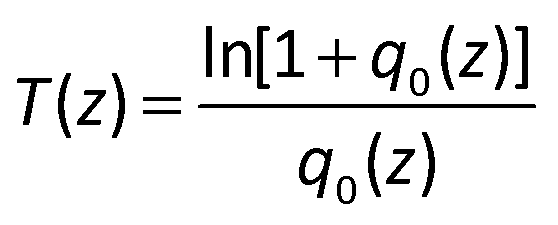
An open-aperture Z-scan system was used to investigate the NLO properties of the hierarchical MoS2 thin films.3,37Total transmittance through the samples as a function of incident intensity was measured while the samples were gradually moved through the focus of a lens along the z-axis. All experiments were performed by using 350 fs laser pulses at 1040 nm with a repetition rate of 100 Hz. The results were fitted using the Z-scan theory and the slow saturable absorber model,38,39
Measurement for Q-switching operation
Q-switching operation has the merits of a tunable repetition frequency of the output pulse train as well as relatively high pulse energy. To demonstrate the saturable absorption of the hierarchical MoS2 nanofilms, the sample was embedded into polyvinyl alcohol (PVA), then the formed MoS2–PVA thin film was incorporated into a fiber laser cavity and the Q-switching operation was obtained. In the laser design, erbium-doped fiber (EDF) was utilized as the gain medium to generate the light near 1550 nm from a continuous wave (cw) laser source. A 976 nm pump was injected into the EDF via a wavelength division multiplexer (WDM). Two polarization controllers were placed inside the cavity to adjust the birefringence for a stable Q-switching operation. The MoS2 sample was embedded between two fiber connectors. A 90![[thin space (1/6-em)]](https://www.rsc.org/images/entities/char_2009.gif) :10 coupler was used to extract the light for output and an isolator was used to guarantee the single-directional operation.
:10 coupler was used to extract the light for output and an isolator was used to guarantee the single-directional operation.
Results and discussion
The synthesis strategy of the hierarchical MoS2 nanofilms is schematically shown in Fig. 1, which includes the formation of horizontally aligned MoS2 layers and the following growth of the vertically aligned MoS2 layers on the defects of the horizontally aligned ones. Here, (NH4)2MoO4 and (NH2)2S are chosen as the molybdenum and sulfur precursors, respectively. NMP is selected as the solvent, as NMP is biodegradable and has a surface energy that matches that of MoS240,41 In contrast to the previous solvothermal/hydrothermal conditions wherein the molybdenum and sulfur precursors were dissolved in the same solvent,34–36 NMP can only dissolve the sulfur precursor, and the molybdenum precursor is dissolved by deionized water. These two compounds finally form a transparent solution, as NMP is miscible with water. In this specially designed system, the reaction is limited in the small amount of water as shown in Fig. 1. The sulfur precursor is excessive in NMP and can gradually diffuse into water along with the reaction process because of which NMP cannot dissolve the molybdenum precursor, thus resulting in a slow reaction rate. It should be mentioned that no MoS2 is generated under the same conditions in a pure water system, which in turn illustrates the advantage of the selected NMP–H2O system. The structural evolution processes of the hierarchical MoS2 nanofilms under the solvothermal conditions can also be observed from the corresponding SEM images in Fig. 1. Clearly, the horizontally aligned MoS2 with lots of defects are firstly formed, and the precursor molecules tend to be adsorbed on these active defect sites. Then the vertically aligned layers grow gradually from the precursor molecules adsorbed by these active defect sites on the horizontal layers, which finally generate the hierarchical structure of the MoS2 thin films.
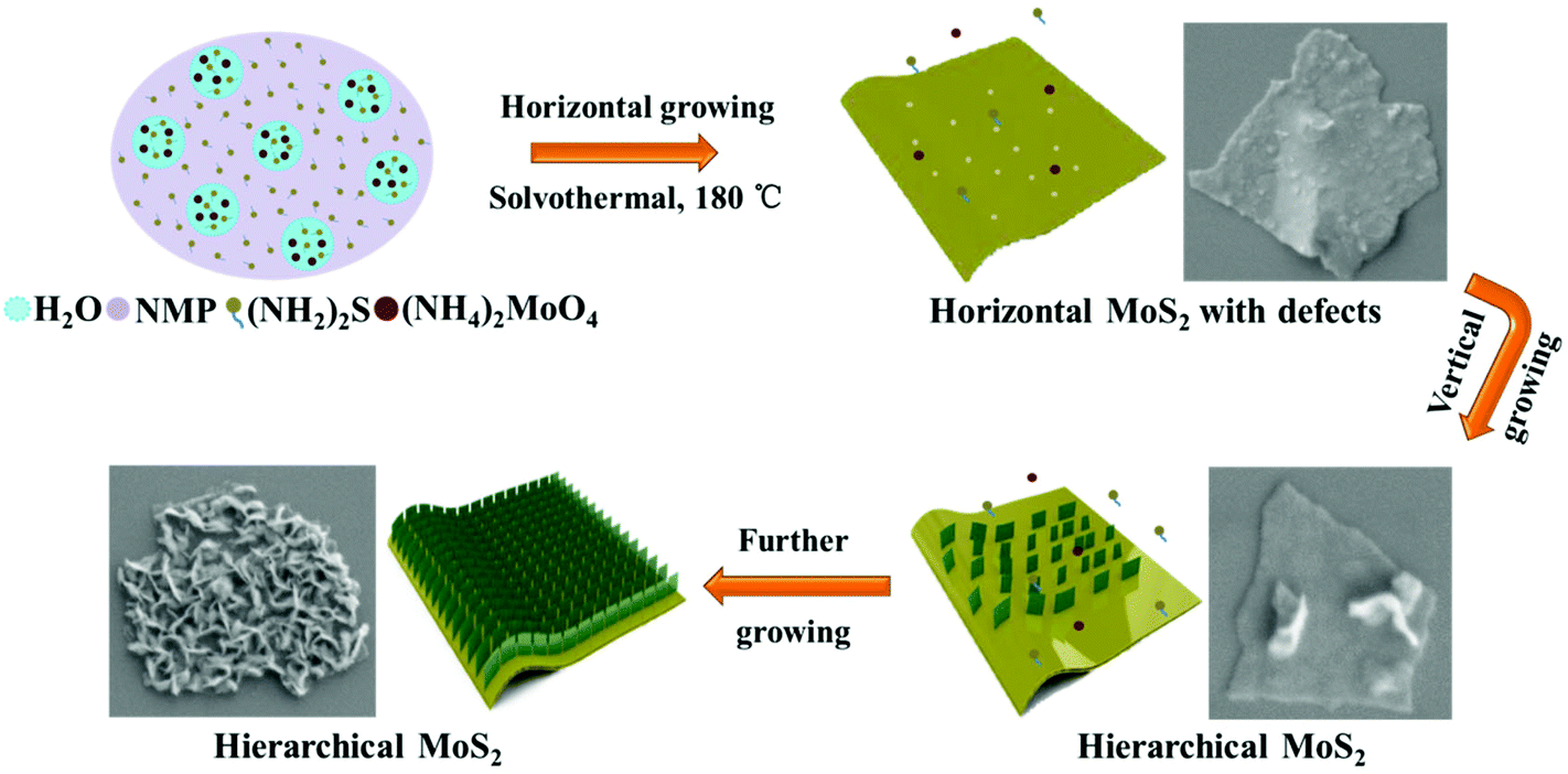 | ||
| Fig. 1 Schematics for the formation of the hierarchical MoS2 nanofilms with vertically aligned layers grown on horizontally aligned layers without any additives. | ||
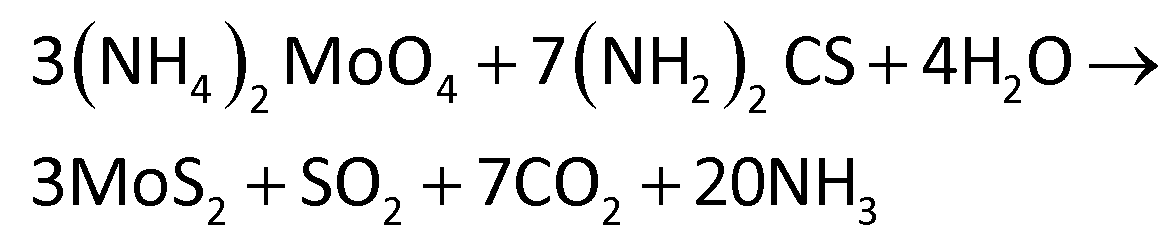
Fig. 2 shows the SEM images of the hierarchical MoS2 nanofilms. Obviously, the surface of the MoS2 thin films displays a unique hierarchical structure (Fig. 2a) with the back side having many defects (Fig. 2b). Both the hierarchical surface and the back side are observed from a piece of curved MoS2 nanoplate as shown in Fig. 2c. It can be concluded that the vertically aligned layers grow on the defects of the horizontally aligned layers, which finally form the hierarchical and orthogonal structure, combined with the cross-sectional SEM image of the MoS2 thin films (Fig. 2d). Typically, the thickness of the horizontal layers is ∼30 nm, and the thickness of the vertical ones is ∼120 nm, resulting in a total thickness ∼150 nm. No MoS2 can be prepared under the exactly same experimental conditions by replacing NMP with water, probably due to the low concentration of the molybdenum precursor. However, in the NMP–H2O system, the concentration of the molybdenum precursor is significantly increased because it can only be dissolved in water. To improve the crystallinity, the samples were annealed under an Ar atmosphere at 800 °C for 2 h. The detailed synthetic reaction is formulated as follows.42
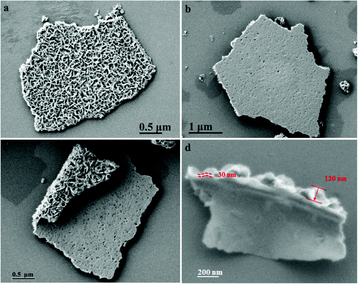 | ||
| Fig. 2 SEM images of (a) the top, (b) the back side, (c) a curved edge and (d) the cross-section of the hierarchical MoS2 nanofilms. | ||
Transmission electron microscopy is used to further characterize the morphology of the hierarchical MoS2 films. Fig. 3a shows the TEM image of the hierarchical MoS2 nanofilms. The nearly vertically aligned nanosheets with approximately 4–8 layers, a d(002) of 0.64 nm and a hexagonal structure were observed (Fig. 3b, c, and inset in Fig. 3c). Fig. 3d reveals the TEM image of a piece of MoS2 nanoplate with loose vertically-aligned layers, which clearly demonstrates the orthogonally oriented vertical/horizontal heterostructure, as indicated by the dashed-line cycle and the solid-line cycle, respectively. The results further prove the growth mechanism of the hierarchical MoS2 thin films consisting of the formation of the horizontally aligned layers and the following growth of the vertically aligned layers. The corresponding energy-dispersive spectrometry (EDS) results confirm that the nanoplates are composed of MoS2 having a Mo/S atomic ratio of ∼2.08 (Fig. S1†), which is also verified by the XPS results (Fig. S2†). It is worth noting that the orthogonal structure for the hierarchical MoS2 thin films can be tuned to possess only horizontally aligned layers by controlling the solvothermal time to 6 h (Fig. 3e). A few-layered structure can be observed from the cross-sectional TEM image of the MoS2 thin films prepared for 6 h, demonstrating that the growth orientation is parallel to the substrate.
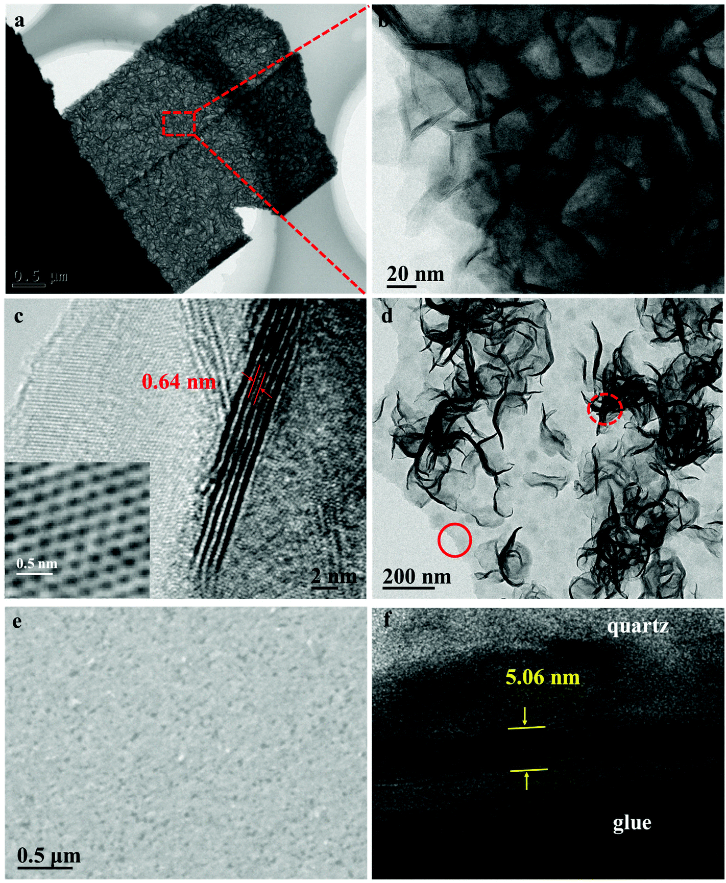 | ||
| Fig. 3 (a) TEM and (b, c) HRTEM images of the hierarchical MoS2 nanofilms. The inset image in (c) is the in-plane TEM of the MoS2. (d) TEM image of a piece of MoS2 nanoplate with loose vertically-aligned layers growing on the horizontally aligned layers, which clearly illustrates the orthogonal structure. The area indicated by the solid-line cycle in (d) is the horizontal layer, and that indicated by the dashed-line cycle is the vertical layer. (e) SEM image and (f) cross-sectional TEM image of the MoS2 thin films with only the horizontally aligned layers obtained by tuning the solvothermal time to be 6 h. | ||
The synthesis of MoS2 thin films with a wafer-scale size is critical for their applications in photonic devices. Thus, the fabrication of continuous large scale MoS2 thin films while retaining the orthogonal nanostructure is urgent. Fig. 4a–c show the hierarchical 2D MoS2 thin films on various substrates, such as fused quartz substrates (Fig. 4a), SiO2/Si substrates (Fig. 4b), and glass substrates with curved surfaces (Fig. 4c). Continuous and uniform thin films can be observed. In particular, uniform hierarchical MoS2 films can also be obtained on the surface of naked optical fibers as shown in Fig. 4d and the inset in Fig. 4d. Such in situ synthesis will allow us to directly fabricate tapered fiber MoS2 saturable absorbers in near future. The AFM image demonstrates that the vertically aligned layers are on the top with a thickness of ∼156 nm (Fig. 4e and f). Good optical homogeneity is observed for the hierarchical MoS2 thin films characterized by a collimated beam from a CW laser light at 532 nm with a diameter of 20 mm (Fig. S3†). This in situ formation of large area and structure-complex thin films as well as free of transfer can greatly lower the cost and complexity of fabrication, and improve the reproducibility, in comparison with the other methods, such as, chemical vapor deposition, physical and chemical exfoliations, etc.
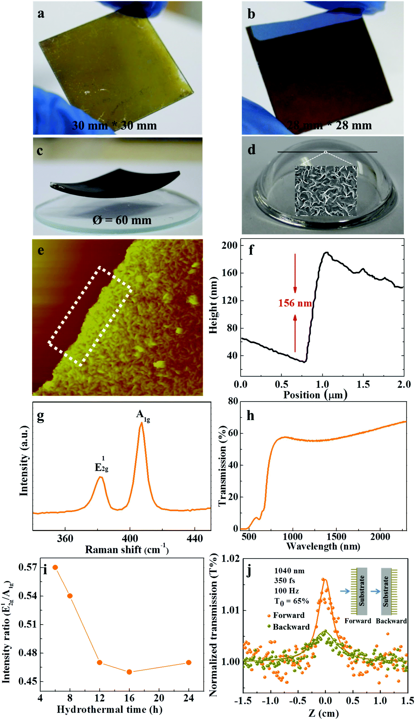 | ||
| Fig. 4 Characterization of the wafer-scale hierarchical MoS2 thin films. Photographs of the films on various substrates, (a) quartz, (b) Si/SiO2, (c) glass with curved surface, and (d) naked optical fibers. The inset in (d) is the magnified SEM image of the nanofilms on the surface of the optical fiber. (e) Typical AFM image of the hierarchical films. (f) The height profile averaged over the white rectangular area in (e). (g) Raman spectrum and (h) transmission spectrum of the hierarchical films. (i) Variation of the intensity ratio E12g/A1g from Raman spectra for the MoS2 thin films prepared with different solvothermal times. (j) Typical Z-scan curves of the hierarchical films with normalized transmission as a function of the sample position Z corresponding to the backward and forward propagation sequences. The inset is the illumination for the sequence of the laser propagation through the films. | ||
Raman and transmission spectra are used to further characterize the structural properties of the hierarchical MoS2 thin films (Fig. 4g and h). The two characteristic Raman peaks E12g (∼382.0 cm−1) and A1g (406.8 cm−1), and two exciton (A and B) absorption peaks of hexagonal MoS2 can be observed. It was reported that the variation of the intensity ratio E12g/A1g is related to the amount of edge sites in layered materials, and a smaller E12g/A1g yields a larger amount of exposed edge sites.29,33 The E12g/A1g was calculated and compared with that for the MoS2 thin films with all horizontal layers, which were fabricated by adjusting the reaction time to 6 h. The calculated E12g/A1g for the hierarchical sample prepared for 24 h is 0.47, much smaller than that of the sample with only horizontal layers prepared for 6 h (Fig. 4i), demonstrating more exposed edges in the hierarchical sample. Similarly, an additional small and broad absorption peak is observed in the near-infrared wavelength region (∼1400 nm) from the transmission spectrum of the hierarchical MoS2 thin films (Fig. 4h, Fig. S4†), further indicating the existence of a large amount of exposed edges.16,43Fig. 4i shows the variation of the intensity ratio E12g/A1g of the Raman spectra as a function of the solvothermal time. Obviously, the E12g/A1g maintains a larger value at short reaction times (5.7 for 6 h, and 5.4 for 8 h), and decreases significantly when the reaction time is prolonged to 12 h, and then remains almost unchanged with increasing reaction time. According to the SEM and TEM results (Fig. 3e and f, Fig. S5†), 6 h of reaction time can only generate horizontally aligned MoS2, the vertical layers begin to appear with 8 h of reaction time, and 12 h of reaction time already generates the hierarchical structure. It should be noted that the sample with the reaction time of 3 h was also prepared, but no MoS2 can be observed from SEM images on the substrates. Besides, we also investigated the effect of the precursor concentrations on the morphology of the samples. It has been revealed that with a lower concentration of molybdenum precursor (0.006 M), hierarchical MoS2 thin films can also be obtained but with lots of impurities on the horizontally aligned layers (Fig. S6†).
Nonlinear optical properties of the continuous hierarchical MoS2 films were investigated using the Z-scan method with a femtosecond pulsed laser at 1040 nm. As shown in Fig. 4j, the sample exhibits an anisotropic saturable absorption response when changing the sequence of a laser beam passing through the vertical layers and the horizontal layers. A larger NLO response was observed when the laser light propagates from the forward side, i.e., the laser light sequentially propagating through the vertical ones and the horizontal layers. Fitting the Z-scan curves indicates that the nonlinear absorption coefficient (βeff) for the forward propagation is ∼50% higher than the backward propagation with the reverse propagation sequence (Table S1†). The different NLO responses are probably due to the enhanced edge-states of the hierarchical MoS2 thin films in the forward propagation configuration.30,33 The hierarchical MoS2 thin films exhibit much larger βeff when compared to that of the liquid-phase exfoliated MoS2 in our previous work,44 which can be attributed to the hierarchical structure with a large amount of exposed edge states.32
In previous studies, 2D MoS2 have been reported to be promising saturable absorption materials that can be used for ultrashort laser pulse generation.3,17,18 Here, the Q-switching operation of the orthogonally layered MoS2 nanofilms is investigated. The Q-switching operation is obtained in a fiber laser based on a MoS2 saturable absorber. The laser setup is shown in Fig. 5a. The MoS2 saturable absorber is embedded between two fiber connectors in the cavity, which is fabricated into the thin films by mixing with a PVA aqueous solution (inset in Fig. 5a). The prepared MoS2–PVA saturable absorber has an insertion loss of ∼34%, a modulation depth of ∼3.1% and a saturation intensity of ∼500 MW cm−2 (Fig. S7a†). The output properties of the Q-switched laser are summarized in Fig. 5b and c. An oscilloscope trace with a very stable pulse amplitude is obtained (Fig. 5b), demonstrating the stable Q-switching operation. Fig. 5c shows the changes in the repetition rates and pulse widths as the pump power increases. The repetition rate varying from 11 kHz to 52 kHz was dependent on the pump power in the range of 80 mW to 300 mW, revealing a low self-starting pump power. The minimum pulse width is 2.2 μs at the pump power of 220 mW. The signal-to-noise ratio at the fundamental repetition rate is 53 dB measured from the RF spectrum at 200 mW pump power (Fig. S7b†). The superior Q-switching operation for the hierarchical MoS2, which is comparable to that of CVD MoS2 and better than that of liquid-phase exfoliated MoS2 (Table S2†), is probably attributed to the large nonlinear absorption induced by the hierarchical structure with a large amount of exposed edge states.32
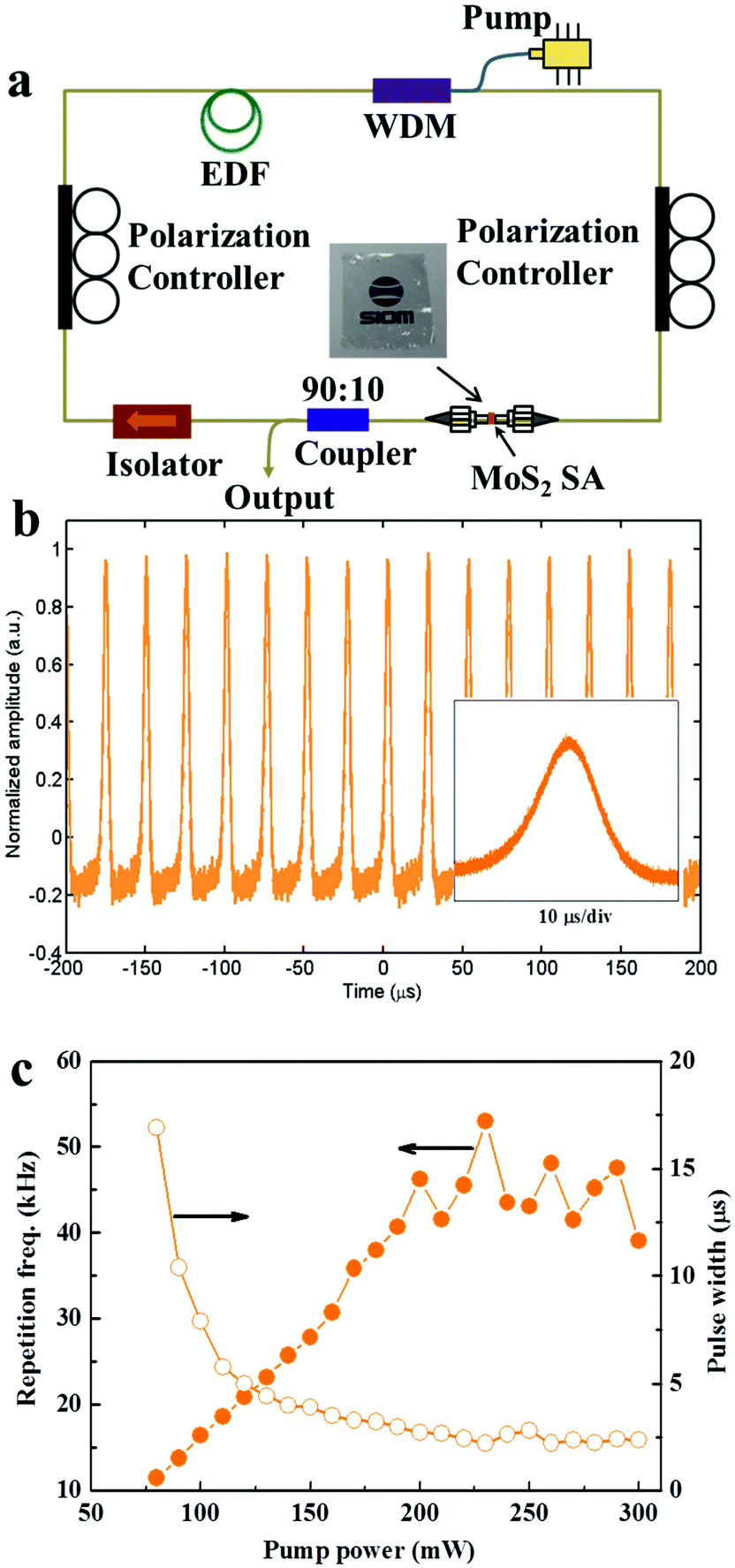 | ||
| Fig. 5 (a) Experimental setup of the fiber laser with MoS2–PVA saturable absorber (SA). (b) Oscilloscope trace and (c) repetition rates and pulse widths with respect to the pump power of the Q-switched laser based on the hierarchical MoS2 nanofilms. The inset shows a zoomed-in image of a single pulse. | ||
Conclusions
In summary, wafer-scale hierarchical MoS2 thin films with orthogonally oriented vertically and horizontally aligned layers were successfully synthesized in a novel reaction system via a simple and green solvothermal method with the assistance of a substrate. The reaction system comprises an organic solvent with a small amount of water wherein the reaction is limited in water and the sulfur precursor gradually diffuses from the organic medium into water to react with the molybdenum precursor. The hierarchical MoS2 thin films with a total thickness of ∼160 nm exhibit anisotropic saturable absorption responses when the laser-propagation sequence was changed. In addition, MoS2 thin films with all horizontally aligned layers are obtained by tuning the solvothermal reaction time. The Q-switching behaviour of the hierarchical MoS2 nanofilms was investigated. A superior passive Q-switching performance in the fiber laser with a minimum pulse width of 2.2 μs was obtained, which is attributed to its unique hierarchical structure consisting of orthogonally oriented vertical/horizontal layers. Our work is expected to prompt the wide applications of TMDs in the photonic and electrochemical fields.Conflict of interest
The authors declare no competing financial interests.Acknowledgements
This work is supported in part by the National Natural Science Foundation of China (no. 51302285, no. 61522510, no. 61178007, no. 61308034), Science and Technology Commission of Shanghai Municipality (no. 12ZR1451800, and the Excellent Academic Leader of Shanghai no. 10XD1404600), and the External Cooperation Program of BIC, CAS (no. 181231KYSB20130007). J.W. thanks the National 10000-Talent Program for financial support, and acknowledges Prof. Werner J. Blau at Trinity College Dublin for his helpful discussion in this work. K. W. thanks Shanghai Yangfan Program (no. 14YF1401600) and the State Key Lab Project of Shanghai Jiao Tong University (no. GKZD030033).Notes and references
- S. Najmaei, Z. Liu, W. Zhou, X. L. Zou, G. Shi, S. D. Lei, B. I. Yakobson, J.-C. Idrobo, P. M. Ajayan and J. Lou, Nat. Mater., 2013, 12, 754–759 CrossRef CAS PubMed.
- M. Chhowalla, H. S. Shin, G. Eda, L.-J. Li, K. P. Loh and H. Zhang, Nat. Chem., 2013, 5, 263–275 CrossRef PubMed.
- K. P. Wang, J. Wang, J. T. Fan, M. Lotya, A. O'Neil, D. Fox, Y. Y. Feng, X. Y. Zhang, B. X. Jiang, Q. Z. Zhao, H. Z. Zhang, J. N. Coleman, L. Zhang and W. J. Blau, ACS Nano, 2013, 7, 9260–9267 CrossRef CAS PubMed.
- X. Huang, Z. Y. Zeng, S. Y. Bao, M. F. Wang, X. Y. Qi, Z. X. Fan and H. Zhang, Nat. Commun., 2013, 4, 1444 CrossRef PubMed.
- J. Kibsgaard, Z. Chen, B. N. Reinecke and T. F. Jaramillo, Nat. Mater., 2012, 11, 963–969 CrossRef CAS PubMed.
- Y. G. Li, H. L. Wang, L. M. Xie, Y. Y. Liang, G. S. Hong and H. J. Dai, J. Am. Chem. Soc., 2011, 133, 7296–7299 CrossRef CAS PubMed.
- F. K. Perkins, A. L. Friedman, E. Cobas, P. M. Campbell, G. G. Jernigan and B. T. Jonker, Nano Lett., 2013, 13, 668–673 CrossRef CAS PubMed.
- D. J. Late, Y.-K. Huang, B. Liu, J. Acharya, S. N. Shirodkar, J. Luo, A. Yan, D. Charles, U. V. Waghmare, V. P. Dravid and C. N. R. Rao, ACS Nano, 2013, 7, 4879–4891 CrossRef CAS PubMed.
- X.-Y. Yu, H. Hu, Y. W. Wang, H. Y. Chen and X. W. Lou, Angew. Chem., Int. Ed., 2015, 54, 7395–7398 CrossRef CAS PubMed.
- X. D. Xu, W. Liu, Y. Kim and J. Cho, Nano Today, 2014, 9, 604–630 CrossRef CAS.
- H. Wang, L. Yu, Y. Lee, Y. Shi, A. Hsu, M. L. Chin, L. Li, M. Dubey, J. Kong and T. Palacios, Nano Lett., 2012, 12, 4674–4680 CrossRef CAS PubMed.
- D. J. Late, B. Liu, H. S. S. R. Matte, C. N. R. Rao and V. P. Dravid, Adv. Funct. Mater., 2012, 22, 1894–1905 CrossRef CAS.
- S. Ghatak, A. N. Pal and A. Ghosh, ACS Nano, 2011, 5, 7707–7712 CrossRef CAS PubMed.
- Z. Yin, H. Li, H. Li, L. Jiang, Y. Shi, Y. Sun, G. Lu, Q. Zhang, X. Chen and H. Zhang, ACS Nano, 2012, 6, 74–80 CrossRef CAS PubMed.
- H. Zhang, S. B. Lu, J. Zheng, J. Du, S. C. Wen, D. Y. Tang and L. P. Loh, Opt. Express, 2014, 22, 7249–7260 CrossRef CAS PubMed.
- S. X. Wang, H. H. Yu, H. J. Zhang, A. Z. Wang, M. W. Zhao, Y. X. Chen, L. M. Mei and J. Y. Wang, Adv. Mater., 2014, 26, 3538–3544 CrossRef CAS PubMed.
- H. Ahmad, F. D. Muhammad, M. Z. Zulkifli and S. W. Harun, Chin. Opt. Lett., 2013, 11, 071401 CrossRef.
- K. Wu, X. Y. Zhang, J. Wang and J. P. Chen, Opt. Lett., 2015, 40, 1374–1377 CrossRef CAS PubMed.
- R. Khazaeizhad, S. H. Kassani, H. Jeong, D.-I. Yeom and K. Oh, Opt. Express, 2014, 22, 23732–23742 CrossRef PubMed.
- J. Du, Q. K. Wang, G. B. Jiang, C. W. Xu, C. J. Zhao, Y. J. Xiang, Y. Chen, S. C. Wen and H. Zhang, Sci. Rep., 2014, 4, 6346 CrossRef CAS PubMed.
- Y. Z. Huang, Z. Q. Luo, Y. Y. Li, M. Zhong, B. Xu, K. J. Che, H. Y. Xu, Z. P. Cai, J. Peng and J. Weng, Opt. Express, 2014, 22, 25258–25266 CrossRef CAS PubMed.
- H. D. Xia, H. P. Li, C. Y. Lan, C. Li, X. X. Zhang, S. J. Zhang and Y. Liu, Opt. Express, 2014, 22, 17341–17348 CrossRef PubMed.
- (a) X. X. Zhang, F. Lou, C. L. Li, X. Zhang, N. Jia, T. T. Yu, J. L. He, B. T. Zhang, H. B. Xia, S. P. Wang and X. T. Tao, CrystEngComm, 2015, 17, 4026–4032 RSC; (b) M. Liu, X.-W. Zheng, Y.-L. Qi, H. Liu, A.-P. Luo, Z.-C. Luo, W.-C. Xu, C.-J. Zhao and H. Zhang, Opt. Express, 2014, 22(19), 22841–22846 CrossRef PubMed; (c) H. Liu, A.-P. Luo, F.-Z. Wang, R. Tang, M. Liu, Z.-C. Luo, W.-C. Xu, C.-J. Zhao and H. Zhang, Opt. Lett., 2014, 39, 4591–4594 CrossRef CAS PubMed; (d) M. Zhang, R. C. T. Howe, R. I. Woodward, E. J. R. Kelleher, F. Torrisi, G. Hu, S. V. Popov, J. R. Taylor and T. Hasan, Nano Res., 2015, 8(5), 1522–1534 CrossRef CAS; (e) H. Xia, H. Li, C. Lan, C. Li, X. Zhang, S. Zhang and Y. Liu, Opt. Express, 2014, 22, 17341–17348 CrossRef PubMed.
- (a) Y. Zhan, L. Wang, J. Y. Wang, H. W. Li and Z. H. Yu, Laser Phys., 2015, 25, 025901 CrossRef CAS; (b) S. Wang, H. Yu, H. Zhang, A. Wang, M. Zhao, Y. Chen, L. Mei and J. Wang, Adv. Mater., 2014, 26, 3538–3544 CrossRef CAS PubMed; (c) B. Xu, Y. Cheng, Y. Wang, Y. Huang, J. Peng, Z. Luo, H. Xu, Z. Cai, J. Weng and R. Moncorgé, Opt. Express, 2014, 22, 28934–28940 CrossRef PubMed; (d) R. I. Woodward, E. J. R. Kelleher, R. C. T. Howe, G. Hu, F. Torrisi, T. Hasan, S. V. Popov and J. R. Taylor, Opt. Express, 2014, 22, 31113–31122 CrossRef CAS PubMed; (e) Y. Huang, Z. Q. Luo, Y. Y. Li, M. Zhong, B. Xu, K. J. Che, H. Y. Xu, Z. P. Cai, J. Peng and J. Weng, Opt. Express, 2014, 22, 25258–25266 CrossRef CAS PubMed; (f) Z. Luo, Y. Huang, M. Zhong, Y. Li, J. Wu, B. Xu, H. Xu, Z. Cai, J. Peng and J. Weng, J. Lightwave Technol., 2014, 32, 4679–4686 CrossRef CAS; (g) R. Khazaeinezhad, S. H. Kassani, T. Nazari, H. Jeong, J. Kim, K. Choi, J.-U. Lee, J. H. Kim, H. Cheong, D.-I. Yeom and K. Oh, Opt. Commun., 2015, 335, 224–230 CrossRef CAS; (h) H. Li, H. Xia, C. Lan, C. Li, X. Zhang, J. Li and Y. Liu, IEEE Photonics Technol. Lett., 2015, 27, 69–72 CrossRef CAS; (i) B. H. Chen, X. Y. Zhang, K. Wu, H. Wang, J. Wang and J. P. Chen, Opt. Express, 2015, 23(20), 23723–26737 Search PubMed.
- R. I. Woodward, R. C. T. Howe, G. Hu, F. Torrisi, M. Zhang, T. Hasan and E. J. R. Kelleher, Photonics Res., 2015, 3(2), A30 CrossRef.
- A. Splendiani, L. Sun, Y. Zhang, T. Li, J. Kim, C.-Y. Chim, G. Galli and F. Wang, Nano Lett., 2010, 10, 1271–1275 CrossRef CAS PubMed.
- K. F. Mak, C. Lee, J. Hone, J. Shan and T. F. Heinz, Phys. Rev. Lett., 2010, 105, 136805 CrossRef PubMed.
- W. Zhao, Z. Ghorannevis, L. Chu, M. Toh, C. Kloc, P.-H. Tan and G. Eda, ACS Nano, 2012, 7, 791–797 CrossRef PubMed.
- D. Kong, H. Wang, J. J. Cha, M. Pasta, K. J. Koski, J. Yao and Y. Cui, Nano Lett., 2013, 13, 1341 CrossRef CAS PubMed.
- J. Kibsgaard, Z. B. Chen, B. N. Reinecke and T. F. Jaramillo, Nat. Mater., 2012, 11, 963–969 CrossRef CAS PubMed.
- H. Hwang, H. Kim and J. Cho, Nano Lett., 2011, 11, 4826–4830 CrossRef CAS PubMed.
- X. B. Yin, Z. L. Ye, D. A. Chenet, Y. Ye, K. O'Brien, J. C. Hone and X. Zhang, Science, 2014, 344, 488–490 CrossRef CAS PubMed.
- Y. Jung, J. Shen, Y. Liu, J. M. Woods, Y. Sun and J. J. Cha, Nano Lett., 2014, 14, 6842–6849 CrossRef CAS PubMed.
- H. S. S. R. Matte, A. Gomathi, A. K. Manna, D. J. Late, R. Datta, S. K. Pati and C. N. R. Rao, Angew. Chem., Int. Ed., 2010, 49, 4059–4062 CrossRef CAS PubMed.
- L. R. Hu, Y. M. Ren, H. X. Yang and Q. Xu, ACS Appl. Mater. Interfaces, 2014, 6, 14644–14652 CAS.
- G. C. Huang, T. Chen, W. X. Chen, Z. Wang, K. Chang, L. Ma, F. H. Huang, D. Y. Chen and J. Y. Lee, Small, 2013, 9, 3693–3703 CrossRef CAS PubMed.
- J. Wang, Y. Hernandez, M. Lotya, J. N. Coleman and W. J. Blau, Adv. Mater., 2009, 21, 2430–2435 CrossRef CAS.
- K. P. Wang, Y. Y. Feng, C. X. Chang, J. X. Zhan, C. W. Wang, Q. Z. Zhao, J. N. Coleman, L. Zhang, W. J. Blau and J. Wang, Nanoscale, 2014, 6, 10530–10535 RSC.
- M. Pokrass, Z. Burshtein, R. Gvishi and M. Nathan, Opt. Mater. Express, 2012, 2, 825–838 CrossRef CAS.
- M. H. Kim, J.-J. Lee, J.-B. Lee and K.-Y. Choi, CrystEngComm, 2013, 15, 4660–4666 RSC.
- J. N. Coleman, M. Lotya, A. O'Neill, S. D. Bergin, P. J. King, U. Khan, K. Young, A. Gaucher, S. De, R. J. Smith, I. V. Shvets, S. K. Arora, G. Stanton, H. Y. Kim, K. Lee, G. T. Kim, G. S. Duesberg, T. Hallam, J. J. Boland, J. J. Wang, J. F. Donegan, J. C. Grunlan, G. Moriarty, A. Shmeliov, R. J. Nicholls, J. M. Perkins, E. M. Grieveson, K. Theuwissen, D. W. McComb, P. D. Nellist and V. Nicolosi, Science, 2011, 331, 568–571 CrossRef CAS PubMed.
- V. O. Koroteev, L. G. Bulusheva, I. P. Asanov, E. V. Shlyakhova, D. V. Vyalikh and A. V. Okotrub, J. Phys. Chem. C, 2011, 115, 21199–21204 CAS.
- C. D. Zhang, A. Johnson, C.-L. Hsu, L.-J. Li and C.-K. Shih, Nano Lett., 2014, 14, 2443–2447 CrossRef CAS PubMed.
- X. Y. Zhang, S. F. Zhang, C. X. Chang, Y. Y. Feng, Y. X. Li, N. N. Dong, K. P. Wang, L. Zhang, W. J. Blau and J. Wang, Nanoscale, 2015, 7, 2978–2986 RSC.
Footnote |
| † Electronic supplementary information (ESI) available. See DOI: 10.1039/c5nr05938k |
| This journal is © The Royal Society of Chemistry 2016 |