
CTAB-assisted synthesis of novel ultrathin MoSe2 nanosheets perpendicular to graphene for the adsorption and photodegradation of organic dyes under visible light†
Yuxin
Wu
,
Mingquan
Xu
,
Xi
Chen
,
Shuanglei
Yang
,
Hanshuo
Wu
,
Jun
Pan
* and
Xiang
Xiong
*
State Key Laboratory for Powder Metallurgy and Central South University, Changsha 410083, China. E-mail: xiongx@csu.edu.cn; jun.pan@csu.edu.cn
First published on 19th November 2015
Abstract
A novel nanostructure of perpendicular ultrathin MoSe2 nanosheets directly grown on graphene was produced by a facile hydrothermal method in the presence of CTAB. The vertically-oriented and ultrathin MoSe2 nanosheets distribute uniformly on the surface of graphene, and the nanosheets are typically 2–3 layers, which is confirmed by TEM and red shift of the A1g Raman peak. In comparison with pure MoSe2 and MoSe2 nanospheres on graphene, vertically oriented MoSe2 nanosheets on graphene show enhanced organic dye adsorption ability and photocatalytic performance in the degradation of MB, RhB and MO under dark conditions and visible light irradiation. The excellent photocatalytic activity may be contributed by the unique perpendicular MoSe2 nanosheets with fully exposed active edges and hybridized with graphene for reduced electron–hole pair recombination.
Introduction
In recent years, waste waters containing toxicity from various kinds of organic dyes, which are widely produced by the textile, printing, food and other industries, have become one of the most pressing environmental problems. Compared to conventional strategies, semiconductor photocatalytic oxidation of organic dyes using solar light is considered to be a green technology.1,2 As a commonly used photocatalyst, TiO2 is studied extensively due to its non-toxicity, high chemical stability and low cost.3–5 However, TiO2 has a large band gap, which leads to a low photocatalytic efficiency. Therefore, tremendous effort has been devoted to exploration of visible-light-responsive photocatalysts, and a series of impressive visible-light-responsive photocatalysts have been reported.6–11Recently, transition metal dichalcogenides (TMDs) with layered structures have been put forward as promising candidate photocatalysts owing to their outstanding catalytic activities associated with their unique 2D nanostructure and abundance.12–16 Analogous to graphite, TMDs have a layered X–M–X sandwich structure (where M can be any metal ions of the IV, V and VI group transition metal elements and X is a chalcogen and can be S, Se or Te).17 Similarly to graphene, a monolayer or a few layers of MX2 can be exfoliated from the bulk counterpart, which has very distinct physical and chemical properties.18–22 Molybdenum disulfide (MoS2) is the most studied example.23–27 When compared to the intensive research on MoS2, MoSe2 is rarely studied for capacitive properties. MoSe2 is considered a potential photocatalyst because of its narrow band gap (1.33–1.72 eV).28 Even so, the photocatalytic activity of MoSe2 is still restricted by some disadvantages, such as low efficiency of light adsorption, a slow rate of charge transfer and high combination probability of the photogenerated electron–hole pairs.
As a semiconductor, the low conductivity of MoSe2 would significantly suppress their photocatalytic performance due to the slow rate of charge transfer and the high combination probability of the photogenerated electron–hole pairs. Interacting MoSe2 with a conductive matrix, especially nano-carbonaceous materials, such as carbon nanotubes, carbon hollow spheres and graphene, could decrease their resistance to some degree.29 Besides the conductivity, through both experimental and theoretical studies, the edges of MoSe2 have been identified as active sites for the photocatalytic reaction,30 whereas the basal surfaces are catalytically inert. Commonly, nanostructured MoSe2 have more active edges compared to the bulk counterpart. Therefore, various strategies including a template-assisted method,31 liquid exfoliation32 and chemical vapor deposition33 have been used to reduce the MoSe2 size down to nanoscale with increasing density of exposed active edges.
However, the edges of the ultrathin MoSe2 are uncoordinated and thermo-dynamically stable, which are easy to curl up and agglomeration as nanoflower-like.34 Additionally, the conductivity between two vertically stacked Se–Mo–Se van der Waals bonded layers is extremely lower than that of the basal plane.35 So far, most of the stacked layers are parallel to the conductive substrate,36,37 limiting the charge transport efficiency along the adjacent edges from the conductive substrate to the active sites.38 One of the most efficient ways is to orient them with the stacked layers perpendicular to the conductive substrates.
Graphene oxide sheets (GOS) have been considered as an effective substrate for the nucleation and subsequent growth of nanomaterials in the liquid-phase approach owing to their abundance of oxygen-containing functional groups on the GOS surface and edges.39,40 Recently, intensive efforts have been devoted to the synthesis of MoSe2/graphene composites by solvothermal methods, which focused on electrocatalytic activity in HER and electrochemical activity as the anode materials of Li-ion batteries. Lately, Tang reported a hydrothermal method to synthesize MoSe2/graphene hybrids, which possessed superior HER activity with the small onset potential of 0.05 V vs. RHE.38 Ma prepared ultrathin MoSe2/graphene hybrids through the ionic liquid-assisted hydrothermal approach and they demonstrated a high Li-storage capacity (∼1100 mA h g−1at 0.1 A g−1).34
However, up to now, research studies on the interaction of MoSe2 and graphene are mainly about the nanoflower-like MoSe2 particles lying flat on graphene, and the effect of vertically oriented MoSe2 nanosheets on graphene hybrids on the photocatalytic activity has not been reported so far. Cui's group fabricated vertically aligned MoSe2 molecular layers on flat substrates through a complex vapor deposition method.35 Thus, the preparation and characterization of the controllable synthesis of vertical MoSe2 nanosheets between graphene layers by a simple hydrothermal method for photocatalysts are highly warranted for both fundamental research and practical application.
Motivated by the above consideration, in this work we used a facile and simple hydrothermal method to fabricate a novel kind of vertically oriented MoSe2 nanosheets in situ grown on reduced graphene oxide for photocatalysis. We have shown that CTAB, a common cationic surface active agent, plays an anchoring role in fixing MoSe2 nanosheets perpendicular to graphene assisted by long-time stirring at mild temperature. Instrumental characterization results demonstrate that ultrathin MoSe2 nanosheets (2–3 layers) are uniformly and perpendicularly grown on GOS. Degradation tests of different organic dyes were conducted to confirm its excellent adsorption ability and photocatalytic activity.
Experimental section
Materials
Natural graphite powder (99.9999%, 200 mesh) was purchased from Alfa Aesar. Ammonium molybdate tetrahydrate ((NH4)6Mo7O24, 90%), selenium powder (99% 200 mesh), hydrazinium hydrated solution (N2H4·H2O, 80%) and hexadecyltrimethyl ammonium bromide (CTAB, 99%) were obtained from Aladdin. All chemicals were used directly without any further purification.Synthesis of MoSe2/rGO heterostructure
Graphene oxide sheets were prepared from natural graphite powder by the modified Hummers’ method.41 Vertically oriented MoSe2 on graphene composites, referred to as MoSe2⊥rGO, were fabricated by a CTAB-assisted hydrothermal method referring to a previous report with some modified experimental conditions.38 In a typical synthesis, 25 mg graphene oxide was dispersed in 40 mL of 0.02 M CTAB solution by stirring at 40 °C in a water bath for 24 hours until a brown homogeneous solution was achieved. In this step, enough stirring and a little higher temperature than room temperature would help CTA+ ions adsorbed on graphene oxide nanosheets to interface completely by electrostatic interaction. At the same time, 1 mM selenium powder was dissolved into 10 mL of 80% N2H4·H2O solution in the open air to prepare the hydrate-Se solution. After enough stirring, a 10 mL solution containing a stoichiometric amount of (NH4)6Mo7O24 was introduced into the suspension of 40 mL CTAB and GO solutions under stirring at room temperature. Subsequently, the hydrazine hydrate-Se solution was added to the above mixture slowly. After that, the mixture was transferred to a 100 mL Teflon-lined autoclave and heated in an oven at 200 °C for 10 hours. After cooling to room temperature naturally, the black precipitates were collected by vacuum filtration, and washed with deionized water for several times. Then the product was dried at 70 °C for several days. Finally, the obtained samples were annealed in a conventional tube furnace at 450 °C under a flowing highly-pure argon atmosphere for 5 hours to increase crystallinity and remove residual selenium powders. For the control experiment, a pure MoSe2 flower-like nanostructure was prepared by a similar process without the graphene oxide and CTAB, and the MoSe2 nanospheres on the graphene nanostructure (MoSe2/rGO) were fabricated by a similar process in the absence of CTAB.Characterization
Morphology analysis was performed with a NOVO NanoSEM 230 field emission scanning electron microscope (FESEM). Transmission electron microscopy and high solution transmission electron microscopy (HRTEM) images were obtained with JEOL JEM-2100F and Tecnai G2 20ST microscopes operating at 200 kV. The X-ray diffraction (XRD) patterns of the samples were recorded on a Richard D/Max 2500 X-ray diffraction instrument with Cu Kα radiation (λ = 0.15405 nm). X-ray photoelectron spectroscopy (XPS) spectra were collected on a Thermo ESCALAB 250G XPS spectrometer. Raman spectra of powder samples were recorded on LabRAM HR Raman microscope with a laser excitation wavelength of 532 nm. The infrared spectra were obtained by Fourier transform infrared spectroscopy (FTIR, Nicolet 6700). Thermogravimetric analysis (TGA) was conducted using a TGA, SDTQ600. N2 adsorption/desorption measurements were performed using a Quantachrome instrument (Quabrasorb SI-3MP) at 77 K.Photocatalytic experiment
The photocatalytic activities of the samples were determined by the degradation of methylene blue (MB), rhodamine B (RhB) as well as methyl orange (MO) under dark conditions and visible light. A 500 W xenon lamp equipped cutoff filter to completely remove any radiation below 420 nm was used as a visible light source. Typically, an aqueous solution of the organic dyes (15 mg L−1, 15 mL) and the sample powder (MoSe2, MoSe2/rGO hybrids or MoSe2⊥rGO, 5 mg each) were placed in a cylindrical quartz vessel, and the solution was first stirred for 30 min in the dark to analyze the adsorption ability of the as-prepared samples. At certain time intervals of irradiation, around 5 mL aliquots were withdrawn, and then centrifuged separated to remove all the catalysts. The filtrates of the solution were analyzed by using a UV-Vis spectrophotometer (Thermo Fisher, Evolution 220). The characteristic UV-Vis absorption of the dyes (λ = 664, 554 and 464 nm for MB, RhB and MO, respectively) was chosen for assessing the degradation process. The degree of degradation was expressed by C/C0, which is the ratio of the temporal dye concentration to the initial dye concentration. The relative concentration (C/C0), i.e. the ratio of the temporal dye concentration to the initial dye concentration, was applied to define the degradation efficiency.Results and discussion
Characterization of MoSe2⊥rGO
Vertically oriented MoSe2 nanosheets on graphene substrate can be illustrated in Scheme 1. Due to abundant oxygen-containing functional groups, such as –OH and –COOH, the graphene oxide nanosheet surfaces are highly negatively charged. As a cationic surfactant, CTAB can be easily adsorbed on the highly negatively charged GOS surface because of strong electrostatic interactions. A stable solution containing CTA+-modified GOS can be obtained by mixing GOS and CTAB solutions under 24 hours stirring at higher temperature (40 °C), which not only prevented the GOS from stacking but also made the surface positively charged. Hence the positively charged CTA+-modified GOS allows Mo7O246− ions to adsorb on the surface to form a Mo7O246−–CTA+–GOS complex when (NH4)6Mo7O24 aqueous solution was introduced into the suspension of CTA+-modified GOS. Under the hydrothermal treatment, in situ reduction of the Mo7O246− and Se powder by N2H4 forms perpendicular MoSe2 nanosheets dispersed in and hybridized with the graphene layers. Simultaneously, GOS was reduced to graphene.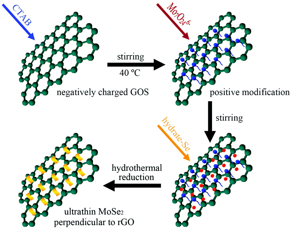 | ||
| Scheme 1 Schematic representation of the synthesis of MoSe2⊥rGO heterostructure. | ||
Field emission scanning electron microscopy (FESEM) images (Fig. 1) clearly showed the morphology of MoSe2⊥rGO heterostructures and MoSe2/rGO composites with different magnifications. As shown in Fig. 1a and c, with the participation of CTAB in the hydrothermal process, ultrathin MoSe2 nanosheets with a curled shape and perpendicular orientation are uniformly distributed on the surfaces of rGO, even on the wrinkles of graphene. The unique architecture with an increased density of exposed active edges can facilitate the charge carrier transfer, which will potentially lead to an enhanced photocatalytic activity, and the FTIR spectra (Fig. S1†) clearly revealed the direct Se–C chemical bonds in MoSe2⊥rGO heterostructures.42 No MoSe2 microspheres were observed, suggesting that the modified graphene sheets could be used as an efficient substrate for the nucleation and growth of perpendicular MoSe2 nanosheets. We also carried out elemental mapping under SEM as shown in Fig. S2,† the homogeneous distribution of selenium (Se) and molybdenum (Mo) elements over the whole area indicated a uniform chemical composition throughout the MoSe2⊥rGO heterostructure. However, serious agglomeration and stacking of sphere-like MoSe2 particles with a mean diameter of about 180 nm were decorated on the surface of graphene as shown in Fig. 1b and d in the absence of CTAB. The sphere-like MoSe2 particles could be thin MoSe2 layers curled up by the high temperature hydrothermal process without in situ growth on the surface of graphene because of the same charged precursors and graphene. And an experiment without long-time stirring on the step of CTAB adsorbing on the GOS surface was also conducted for comparison. As shown in Fig. S3,† perpendicular MoSe2 nanosheets and MoSe2 microspheres coexist on the GOS, which indicated that stirring plays a key role in the modification of GOS.
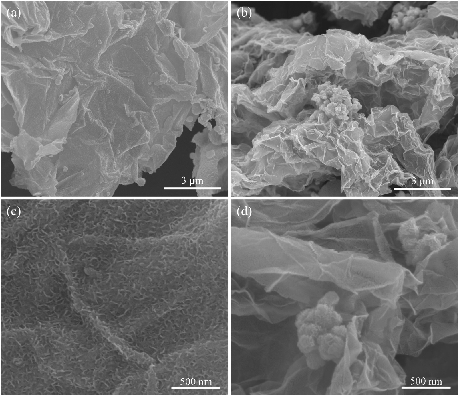 | ||
| Fig. 1 SEM images of the as-prepared (a, c) MoSe2⊥rGO heterostructures and (b, d) MoSe2/rGO composites. | ||
The morphology and microstructure of as-prepared samples were inspected in detail by TEM and HR-TEM observations. The low-magnification TEM images showed a completely different distribution of MoSe2 on the ultrathin rGO nanosheets (Fig. 2a and b). High-magnification TEM images of MoSe2⊥rGO heterostructures (Fig. 2c and d) clearly revealed that the perpendicular MoSe2 nanosheets are grown uniformly on GOS with a large number of exposed sites. And the STEM images of MoSe2⊥rGO heterostructures further confirmed the perpendicular nanosheets of MoSe2 on the graphene surface (Fig. S4†). An individual sheet is typically composed of 2–3 layers of MoSe2 with an interlayer spacing of 0.646 nm, corresponding to the (002) lattice spacing of MoSe2. Fig. 2d further showed the MoSe2 nanosheets in the planar orientation with the d spacing of 0.285 nm matching well with the interspace of the (100) planes of 2H-MoSe2. As shown in the corresponding selected area electron diffraction (SAED) pattern (Fig. 2e), a series of diffraction rings have resulted from the hexagonal MoSe2 phase with a polycrystalline structure and corresponded to the (110), (103) and (100) planes of MoSe2 respectively. The BET analysis (Fig. S5†) showed that the specific surface areas of pure MoSe2, MoSe2/rGO composites and MoSe2⊥rGO heterostructures were 22.68 m2 g−1, 31.49 m2 g−1 and 52.35 m2 g−1. respectively.
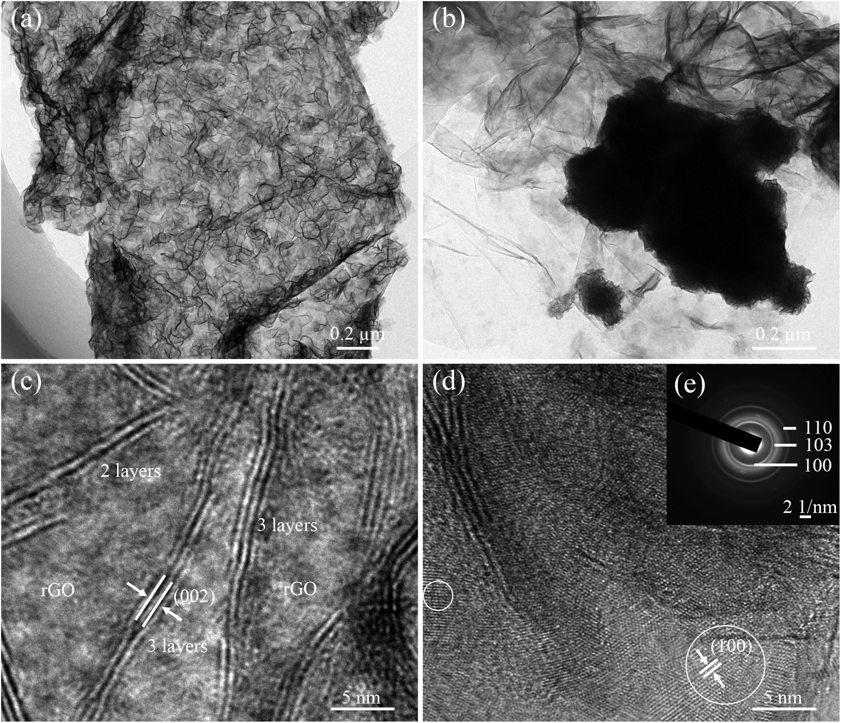 | ||
| Fig. 2 TEM images of (a) the MoSe2⊥rGO heterostructure and (b) MoSe2/rGO composites. HRTEM images of (c, d) the MoSe2⊥rGO heterostructure and (e) the corresponding SAED image. | ||
MoSe2⊥rGO heterostructures were prepared by the facile hydrothermal and subsequent heat-treatment processes. The compositions of pure MoSe2, MoSe2/rGO hybrid and MoSe2⊥rGO heterostructure were firstly characterized by XRD. As shown in Fig. 3, the four diffraction peaks of all three samples centered around 2θ = 13.7, 31.4, 37.9 and 55.9° correspond respectively to the (002), (100), (103) and (110) planes of the hexagonal 2H-MoSe2 (JCPDS Card No. 29-0914). The diffraction peaks in the samples were weaker and broader than standard peaks, indicating that MoSe2 nanosheets of the as-prepared samples were ultrathin and showed low crystallinity. Compared to pure MoSe2 and MoSe2/rGO, the (002) peaks of MoSe2⊥rGO almost disappear, which can be attributed to the fact that the morphology of the vertically oriented MoSe2 nanosheets on graphene decreased the stacking of the MoSe2 layers.34 Moreover, the (002) peak of rGO for MoSe2⊥rGO was not obvious compared with MoSe2/rGO, which may be ascribed to the fact that during the water bath process and the hydrothermal reaction, the modifying effect of the surfactant as well as in situ growth of MoSe2 between the interlayers of GO destroyed the regular layer stacking, leading to the exfoliation of GO and the disappearance of the (002) diffraction peak. The TG curves indicated that the mass loading of MoSe2/rGO composites and MoSe2⊥rGO heterostructures showed almost no difference (Fig. S6†).
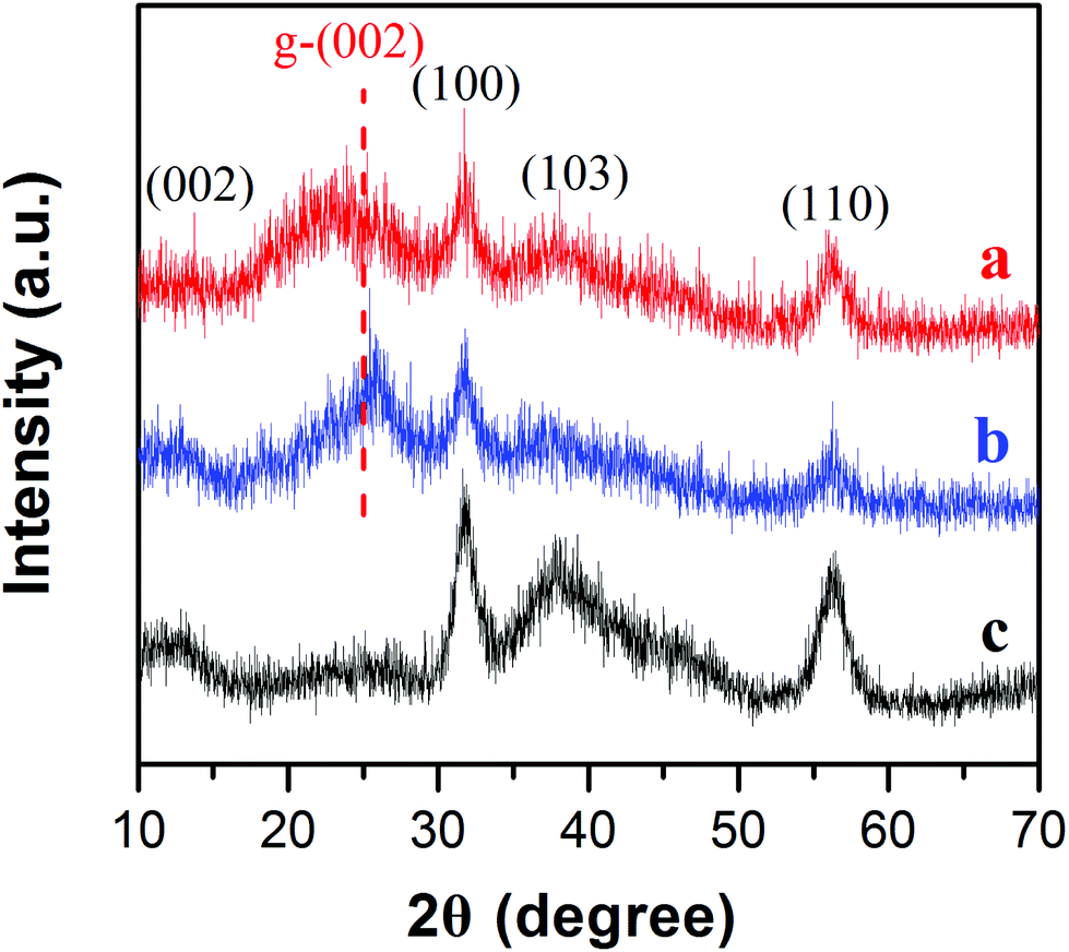 | ||
| Fig. 3 XRD patterns of the as-prepared (a) MoSe2⊥rGO heterostructure, (b) MoSe2/rGO composites and (c) pure MoSe2. | ||
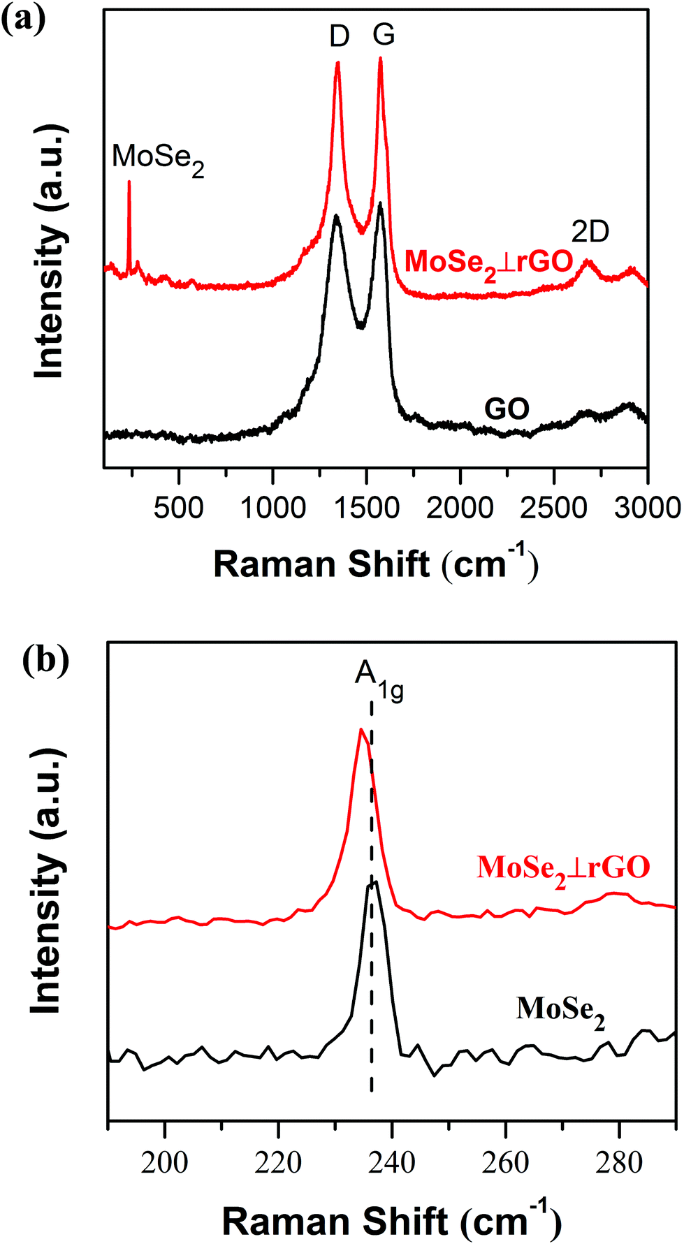
Raman spectroscopy, regarded as one of the most sensitive and universal techniques to characterize layered materials, was employed for the structure of pure MoSe2, GO and MoSe2⊥rGO. Fig. 4a showed two dominant Raman peaks both in GO and MoSe2⊥rGO heterostructure near 1348 cm−1 and 1571 cm−1, which correspond to D and G bands of graphene, respectively.43 The G band is attributed to the vibration of sp2 carbon atoms in a 2D hexagonal lattice, and the D mode is associated with defects or lattice distortion. Commonly, the relative intensity ratio ID/IG is an indication of the graphene quality.44 The ID/IG value for the MoSe2⊥rGO heterostructure (ID/IG = 1.64) was smaller than that for GO (ID/IG = 1.74), indicating the simultaneous reduced reaction via a hybridization process. Additionally, a 2D band at 2684 cm−1 was also observed in the heterostructures, which was also indicative of the reduction of GO and the formation of graphene. The Raman spectrum in Fig. 4b, in the informative range from 190 to 290 cm−1, displayed the characteristic peak of MoSe2. The typical peaks of pure MoSe2 and MoSe2⊥rGO were observed at 236.7 and 234.9 cm−1, respectively, corresponding to the out-of-plane A1g mode of MoSe2.45 The red shift of the MoSe2⊥rGO heterostructure compared with pure MoSe2 nanosheets and bulk MoSe2 indicated that the MoSe2 nanosheets in the heterostructure are ultrathin few layers.46 The absence of the in-plane (E12g) mode is probably due to the high intensity ratio between the A1g and E12g modes, also suggesting a few-layer structure and relatively weak layer–layer interactions in the as-prepared samples.
 | ||
| Fig. 4 (a) Raman spectra of GO and MoSe2⊥rGO heterostructure and (b) Raman spectra of pure MoSe2 and MoSe2⊥rGO heterostructure in the range of 190–290 cm−1. | ||
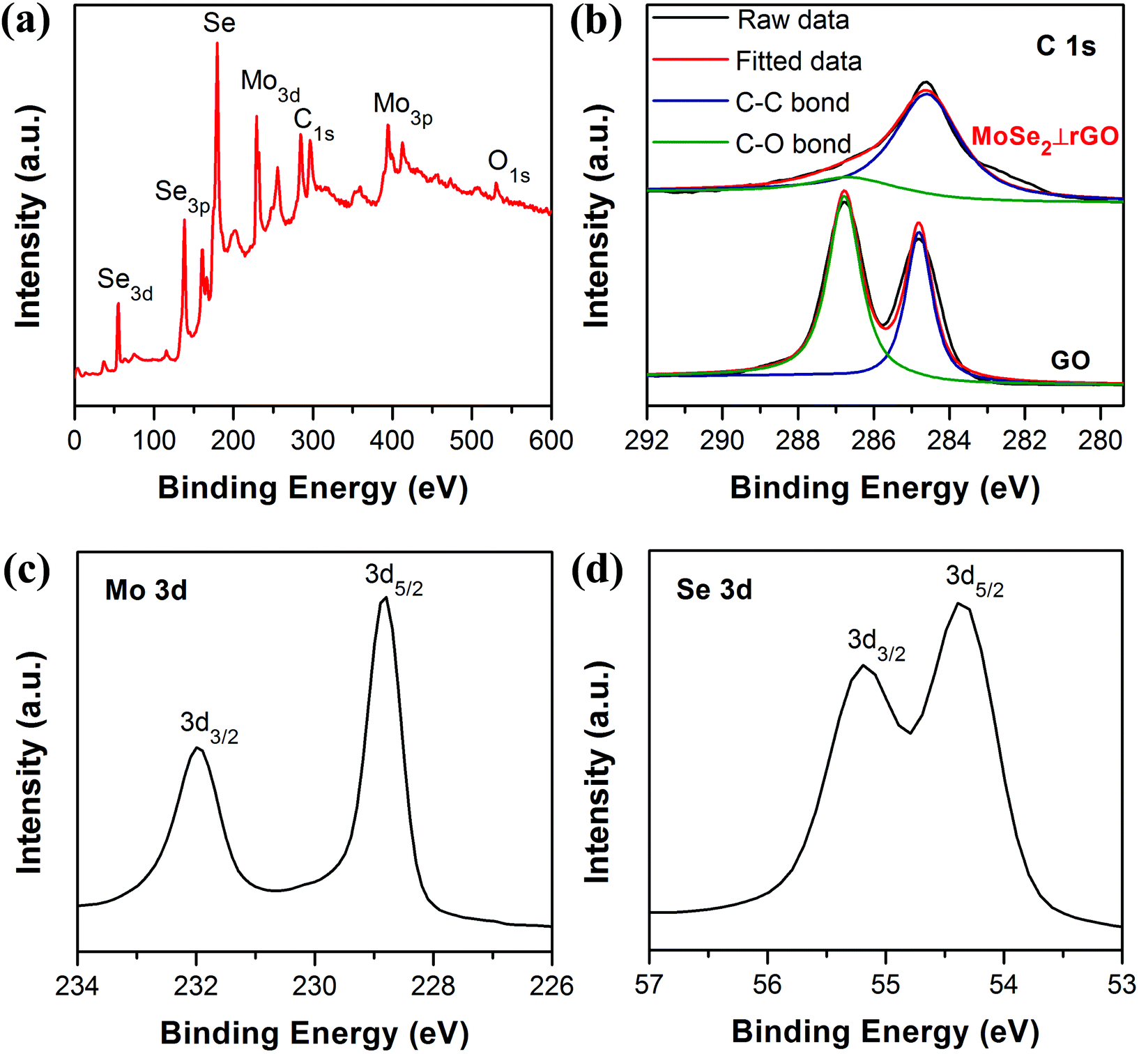
In order to further investigate the chemical composition and oxidation state of samples, X-ray photoelectron spectroscopy (XPS) was carried out. From the spectrum of Fig. 5a, the elements Mo, C, O, and Se can be clearly identified. The C 1s spectra (Fig. 5b) indicated a decrease of oxygen content in MoSe2⊥rGO compared with that of GO. The spectrum of GO featured peaks at 284.8 and 286.8 eV respectively, corresponding to C–C and C–O bonds. The MoSe2⊥rGO spectrum had dominant C–C peaks with much weaker C–O peaks, suggesting considerable deoxygenation of GO to rGO through the hydrothermal process. Two peaks appearing at binding energies of 228.95 and 232.09 eV (Fig. 5c) can be ascribed to Mo 3d5/2 and Mo 3d3/2, respectively, revealing the +4 oxidation state of molybdenum.47,48 Meanwhile, Se 3d5/2 and Se 3d3/2 peaks were located at 54.43 and 55.28 eV, indicating the −2 oxidation chemical state of Se in the nanosheets.49
 | ||
| Fig. 5 XPS of the as-prepared samples. (a) Survey spectra of MoSe2⊥rGO. (b) High resolution C 1s spectra of GO and MoSe2⊥rGO. High resolution (c) Mo 3d and (d) Se 3d spectra of MoSe2⊥rGO heterostructure. | ||
Adsorption ability and photocatalytic activity
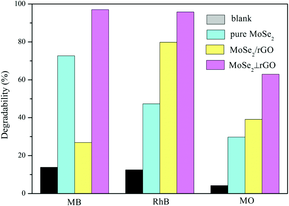
To evaluate the adsorption and photocatalytic performance, the degree of MB, RhB and MO degradation under dark conditions and visible light irradiation was measured for the as-prepared MoSe2⊥rGO heterostructure sample compared with that of pure MoSe2 and MoSe2/rGO composites. MB, RhB and MO were selected as different types of model pollutants because they are common poisonous contaminants in industrial wastewater and sanitary sewage. We also recorded the adsorption spectra of three organic dyes under dark conditions for 60 minutes.50 The concentration of the three dyes shows no significant decrease after 30 min in the dark from the adsorption data (Fig. S7†). Therefore, we investigated the photocatalytic activity under visible light after the dark adsorption process for 30 min.Fig. 6a–c shows the time-dependent degradation curves of MB, RhB and MO, respectively, as well as the blank sample. These dyes hardly undergo self-degradation under visible light without a catalyst, confirming their good chemical stability. In the beginning, the organic dye solutions with as-prepared samples were stirred in the dark for 30 min to examine their adsorption abilities. We can observe that the MoSe2⊥rGO heterostructures show higher adsorption ability to all three dyes than pure MoSe2 and MoSe2/rGO samples. This phenomenon may have a relationship with the larger surface area of MoSe2⊥rGO heterostructures due to less re-stacking and agglomeration of MoSe2 and rGO nanosheets. The MoSe2⊥rGO samples exhibited a significantly higher efficiency for all three dyes than pure MoSe2 and MoSe2/rGO after adsorption under dark conditions and visible light irradiation. Fig. 7 shows in detail the degradation percentage of the dyes after the processes. For MoSe2⊥rGO, almost all MB and RhB as well as 62.1% MO were removed, leading to a marked promotion compared with pure MoSe2 and MoSe2/rGO. MoSe2/rGO presented much weaker photocatalytic activity compared with MoSe2⊥rGO, which further confirmed the optimized heterostructure with more uniform distribution of perpendicular MoSe2 nanosheets and exposed much more active edge sites.
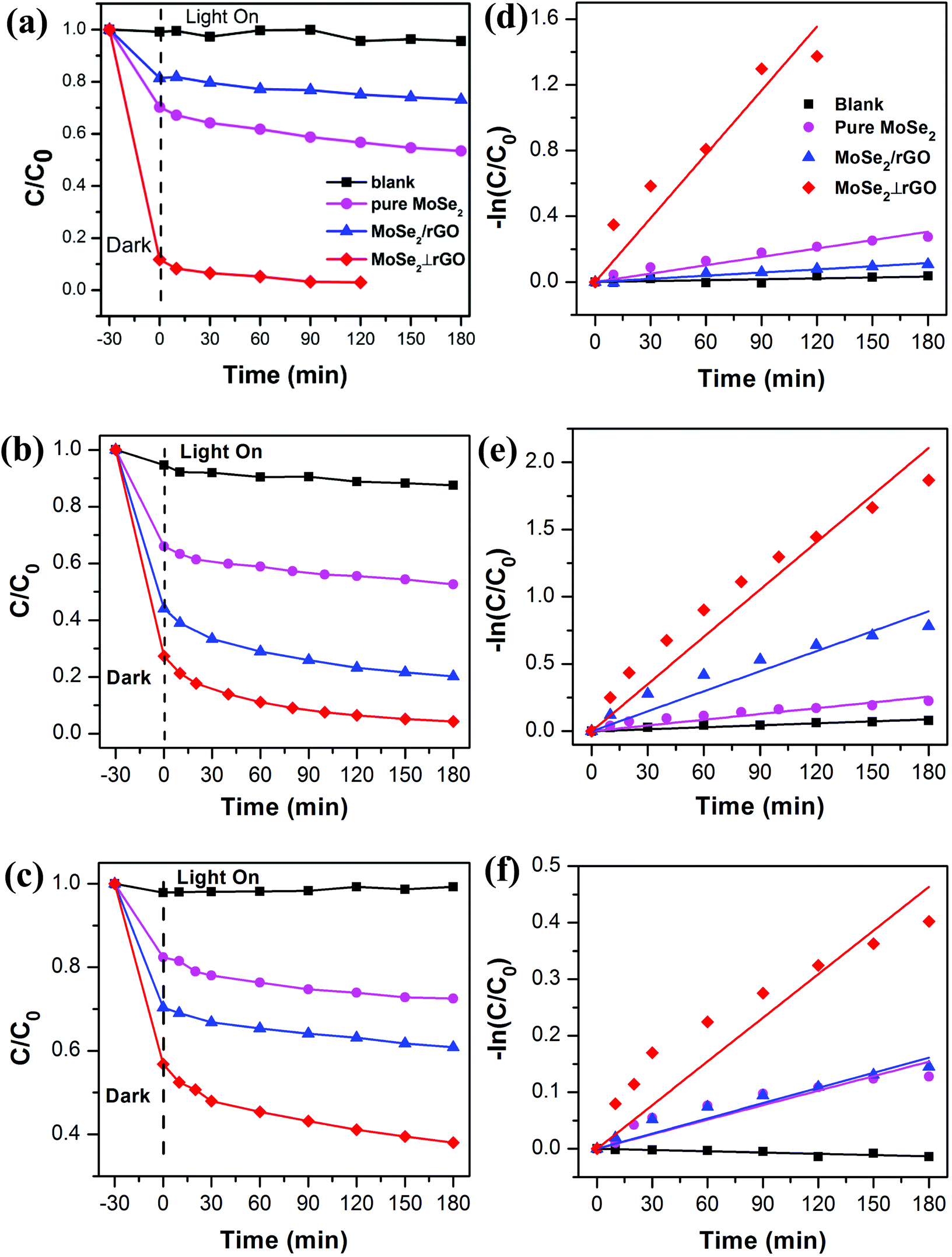 | ||
| Fig. 6 Photocatalytic activity of different samples (a–c) and variation in −ln(C/C0) as a function of irradiation time and linear fits of different samples (d–f). C0 and C represent the initial concentration of dyes and the concentration at time t, respectively. The legends of (b, c, e, and f) are the same as those of (a and d). | ||
 | ||
| Fig. 7 Different organic dyes’ degradability distribution for as-prepared samples under dark conditions and visible light irradiation. | ||
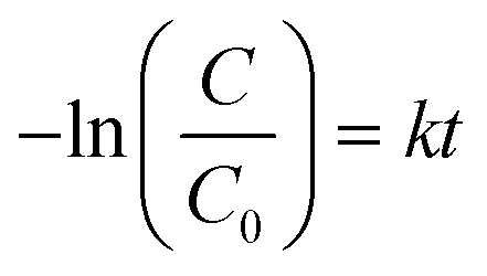
To quantitatively investigate the photodegradation rate under visible light by the as-prepared photocatalysts, the experimental data were analyzed using the pseudo-first-order equation as follows:
 | (1) |
| Sample k (min−1) | Blank | Pure MoSe2 | MoSe2/rGO | MoSe2⊥rGO |
|---|---|---|---|---|
| MB | 1.823 × 10⁻⁴ | 0.0017 | 6.380 × 10⁻⁴ | 0.01296 |
| RhB | 4.911 × 10⁻⁴ | 0.00143 | 0.00496 | 0.01171 |
| MO | 7.357 × 10⁻⁵ | 8.570 × 10⁻⁴ | 8.971 × 10⁻⁴ | 0.00257 |
It could be clearly seen that the rate constant of MoSe2⊥rGO was larger than those of pure MoSe2 and MoSe2/rGO samples, which suggested the presence of a synergistic effect between the two components. Taking the degradation of MB as an example, the apparent rate constant of MoSe2⊥rGO (0.0130 min−1) was almost 7.6 and 20.3 times that of pure MoSe2 and MoSe2/rGO respectively.
Possible photocatalytic mechanism
To reveal the photocatalytic mechanism in the photocatalytic process of MB over MoSe2⊥rGO heterostructure, trapping experiments were performed to investigate the roles of active species. The sacrificial agents, including benzoquinone (BQ), ethylene diamine teraacetic acid disodium (EDTA-2Na) and isopropanol (IPA), were added as the scavengers for superoxide radicals (˙O2−), holes (h+), and hydroxyl radicals (˙OH) respectively. Fig. 8 shows the variation of MB degradation for different quenchers. The degradation efficiency of MB almost had no effect in the presence of BQ, indicating that very few ˙O2− species were involved in the degradation process. On the contrary, the degradation rate for MB significantly decreased with the addition of IPA or EDTA-2Na, which implies that h+ and ˙OH played a major role in MoSe2⊥rGO under visible irradiation.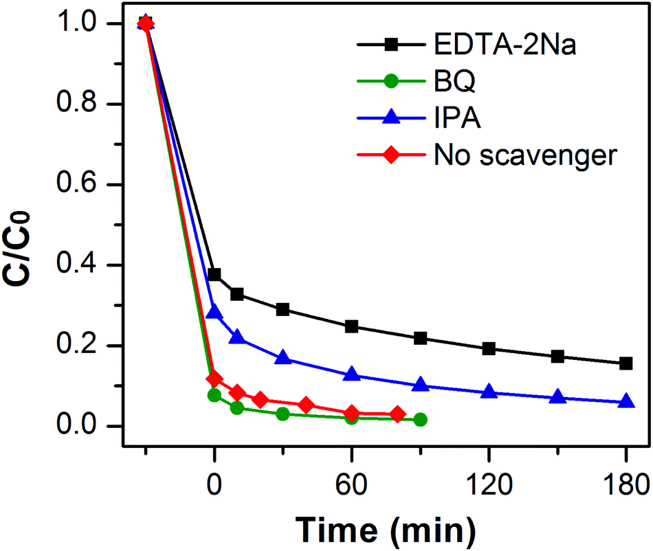 | ||
| Fig. 8 Photodegradation of MB over MoSe2⊥rGO photocatalyst in the presence of different scavengers. | ||
Based on the above results, a possible mechanism assumed for the degradation of MB dyes by MoSe2⊥rGO heterostructures is proposed and illustrated in Scheme 2. Under visible light irradiation, the electrons of MoSe2 can be promoted from the valence band to the conducting band, leaving behind a hole in the valence band. Due to the fact that the conducting band of MoSe2 (ca. −3.8 eV)28 is smaller than the work function of graphene (4.42 eV),51 graphene as a reservoir accepting photogenerated electrons is thermodynamically favorable. Additionally, the 2D planar structure endows graphene with superior electrical conductivity.52,53 Furthermore, because of the vertically oriented morphological MoSe2 and the strong interfacial interactions between MoSe2 nanosheets and graphene, originating from the in situ growth, photogenerated electrons are easy to transfer from the MoSe2 onto the surface of graphene. Owing to the fact that the conduction band of MoSe2 is largely positive compared to the normal hydrogen electrode (NHE), there are plentiful H+ ions in solutions. These electrons further react with O2 adsorbed on the surface of graphene to fabricate abundant ˙O2−, then ˙O2− can continue to oxidize the H+ ions in solutions to produce active radicals with a powerful oxidization (˙O2− + 2H+ + 2e− → ˙OH + OH−). And the holes in the VB of MoSe2 could directly oxidize organic pollutants into CO2, H2O and other intermediates. Therefore, the vertically oriented MoSe2–graphene nano-architectures could greatly facilitate the separation of photogenerated charge carriers and effectively suppress the recombination of electrons and holes, resulting in an increase in the number of holes and ˙OH radicals as active species participating in the photooxidation process. Meanwhile, the morphology of vertically oriented MoSe2 on graphene increases the surface active sites as well as the surface adsorption ability of the photocatalyst system, which are also beneficial for the photocatalytic reaction.
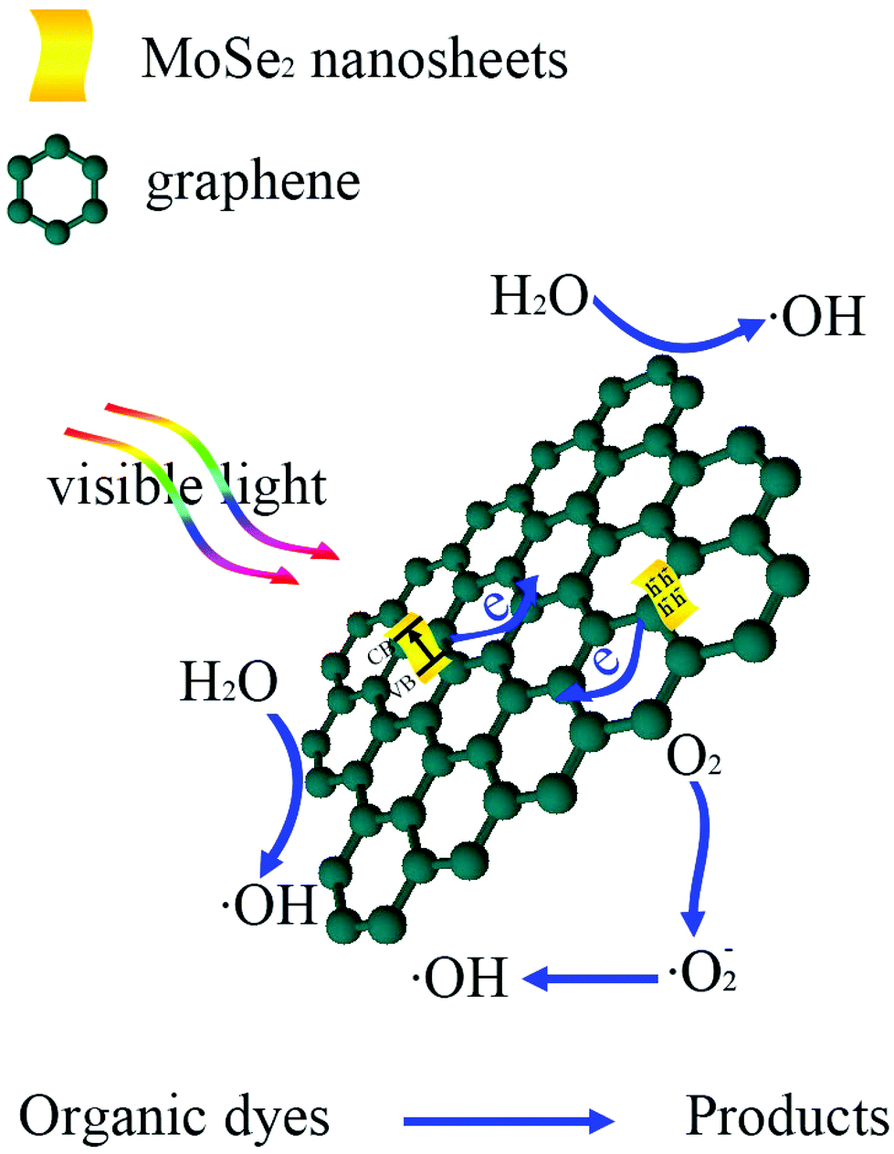 | ||
| Scheme 2 Schematic illustration of the transfer route of the photoinduced charge carrier and the possible photocatalytic mechanism of the MoSe2⊥rGO heterostructure under visible light irradiation. | ||
Conclusion
In summary, a hydrothermal method after long-time stirring with GO and CTAB has been developed for the successful synthesis of vertically oriented ultrathin MoSe2 nanosheets on graphene. During the synthesis process, CTAB plays a key role in the modification of the inherent negative-charged GOS surface, and graphene efficiently inhibits the aggregation of MoSe2. Due to the ultrathin (2–3 layers) and perpendicular MoSe2, active edges in the heterostructure are abundant. The heterostructure shows an excellent photocatalytic activity in the degradation of different organic dyes. Its high surface area leads to excellent adsorption ability; both high conductivity and more exposed active edges are the reason for enhanced photocatalytic activity, making it a promising candidate for degradation of organic pollutants.Acknowledgements
We gratefully acknowledge financial support from the National Science Foundation of China (51302325), Science Fund for Distinguished Young Scholars of Hunan Province(2015JJ1016), Program for New Century Excellent Talents in University (NECT-12-0553), the fund of the State Key Laboratory of Advanced Technologies for Comprehensive Utilization of Platinum Metals (SKL-SPM-201507), the Scientific Research Foundation for the Returned Oversea China Scholars, the Hunan Youth Innovation Platform and Program for Shenghua Overseas Talent (90600-903030005; 90600-996010162) from Central South University (CSU).References
- C. Chen, W. Ma and J. Zhao, Chem. Soc. Rev., 2010, 39(11), 4206–4219 RSC.
- M. R. Hoffmann, S. T. Martin, W. Choi and D. W. Bahnemann, Chem. Rev., 1995, 95(1), 69–96 CrossRef CAS.
- J. B. Joo, Q. Zhang, M. Dahl, I. Lee, J. Goebl, F. Zaera and Y. Yin, Energy Environ. Sci., 2012, 5(4), 6321–6327 CAS.
- G. Wang, H. Wang, Y. Ling, Y. Tang, X. Yang, R. C. Fitzmorris, C. Wang, J. Z. Zhang and Y. Li, Nano Lett., 2011, 11(7), 3026–3033 CrossRef CAS PubMed.
- H. Ming, Z. Ma, H. Huang, S. Lian, H. Li, X. He, H. Yu, K. Pan, Y. Liu and Z. Kang, Chem. Commun., 2011, 47(28), 8025–8027 RSC.
- X. Chen, L. Liu, P. Y. Yu and S. S. Mao, Science, 2011, 331(6018), 746–750 CrossRef CAS PubMed.
- S. Wang, C. Li, T. Wang, P. Zhang, A. Li and J. Gong, J. Mater. Chem. A, 2014, 2(9), 2885–2890 CAS.
- H. Liu, W. Cao, Y. Su, Y. Wang and X. Wang, Appl. Catal., B, 2012, 111–112, 271–279 CrossRef CAS.
- Y. Cui, J. Briscoe and S. Dunn, Chem. Mater., 2013, 25(21), 4215–4223 CrossRef CAS.
- J. Pan, J. Li, Z. Yan, B. Zhou, H. Wu and X. Xiong, Nanoscale, 2013, 5(7), 3022–3029 RSC.
- X. Chen, B. Zhou, S. Yang, H. Wu, Y. Wu, L. Wu, J. Pan and X. Xiong, RSC Adv., 2015, 5(84), 68953–68963 RSC.
- Q. Xiang, J. Yu and M. Jaroniec, J. Am. Chem. Soc., 2012, 134(15), 6575–6578 CrossRef CAS PubMed.
- W. Zhou, Z. Yin, Y. Du, X. Huang, Z. Zeng, Z. Fan, H. Liu, J. Wang and H. Zhang, Small, 2013, 9(1), 140–147 CrossRef CAS PubMed.
- B. Mahler, V. Hoepfner, K. Liao and G. A. Ozin, J. Am. Chem. Soc., 2014, 136(40), 14121–14127 CrossRef CAS PubMed.
- J. Chen, X.-J. Wu, L. Yin, B. Li, X. Hong, Z. Fan, B. Chen, C. Xue and H. Zhang, Angew. Chem., Int. Ed., 2015, 54(4), 1210–1214 CrossRef CAS PubMed.
- Z. Yin, B. Chen, M. Bosman, X. Cao, J. Chen, B. Zheng and H. Zhang, Small, 2014, 10(17), 3537–3543 CrossRef CAS PubMed.
- H. Wang, H. Yuan, S. Hong, Y. Li and Y. Cui, Chem. Soc. Rev., 2015, 44(9), 2664–2680 RSC.
- M. Chhowalla, Z. Liu and H. Zhang, Chem. Soc. Rev., 2015, 44(9), 2584–2586 RSC.
- X. Huang, Z. Zeng and H. Zhang, Chem. Soc. Rev., 2013, 42(5), 1934–1946 RSC.
- H. Li, J. Wu, Z. Yin and H. Zhang, Acc. Chem. Res., 2014, 47(4), 1067–1075 CrossRef CAS PubMed.
- Z. Zeng, Z. Yin, X. Huang, H. Li, Q. He, G. Lu, F. Boey and H. Zhang, Angew. Chem., Int. Ed., 2011, 50(47), 11093–11097 CrossRef CAS PubMed.
- Z. Zeng, T. Sun, J. Zhu, X. Huang, Z. Yin, G. Lu, Z. Fan, Q. Yan, H. H. Hng and H. Zhang, Angew. Chem., Int. Ed., 2012, 51(36), 9052–9056 CrossRef CAS PubMed.
- Y.-H. Lee, X.-Q. Zhang, W. Zhang, M.-T. Chang, C.-T. Lin, K.-D. Chang, Y.-C. Yu, J. T.-W. Wang, C.-S. Chang, L.-J. Li and T.-W. Lin, Adv. Mater., 2012, 24(17), 2320–2325 CrossRef CAS PubMed.
- G. S. Bang, K. W. Nam, J. Y. Kim, J. Shin, J. W. Choi and S.-Y. Choi, ACS Appl. Mater. Interfaces, 2014, 6(10), 7084–7089 CAS.
- B. Zhu, B. Lin, Y. Zhou, P. Sun, Q. Yao, Y. Chen and B. Gao, J. Mater. Chem. A, 2014, 2(11), 3819–3827 CAS.
- Z. Yin, H. Li, H. Li, L. Jiang, Y. Shi, Y. Sun, G. Lu, Q. Zhang, X. Chen and H. Zhang, ACS Nano, 2012, 6(1), 74–80 CrossRef CAS PubMed.
- H. Li, G. Lu, Z. Yin, Q. He, H. Li, Q. Zhang and H. Zhang, Small, 2012, 8(5), 682–686 CrossRef CAS PubMed.
- J. Kang, S. Tongay, J. Zhou, J. Li and J. Wu, Appl. Phys. Lett., 2013, 102(1), 012111 CrossRef.
- C. Tan and H. Zhang, Chem. Soc. Rev., 2015, 44(9), 2713–2731 RSC.
- C. Tsai, K. Chan, F. Abild-Pedersen and J. K. Norskov, Phys. Chem. Chem. Phys., 2014, 16(26), 13156–13164 RSC.
- Y. Shi, C. Hua, B. Li, X. Fang, C. Yao, Y. Zhang, Y.-S. Hu, Z. Wang, L. Chen, D. Zhao and G. D. Stucky, Adv. Funct. Mater., 2013, 23(14), 1832–1838 CrossRef CAS.
- J. N. Coleman, M. Lotya, A. O'Neill, S. D. Bergin, P. J. King, U. Khan, K. Young, A. Gaucher, S. De, R. J. Smith, I. V. Shvets, S. K. Arora, G. Stanton, H.-Y. Kim, K. Lee, G. T. Kim, G. S. Duesberg, T. Hallam, J. J. Boland, J. J. Wang, J. F. Donegan, J. C. Grunlan, G. Moriarty, A. Shmeliov, R. J. Nicholls, J. M. Perkins, E. M. Grieveson, K. Theuwissen, D. W. McComb, P. D. Nellist and V. Nicolosi, Science, 2011, 331(6017), 568–571 CrossRef CAS PubMed.
- J. Shaw, H. Zhou, Y. Chen, N. Weiss, Y. Liu, Y. Huang and X. Duan, Nano Res., 2014, 7(4), 511–517 CrossRef CAS.
- L. Ma, X. Zhou, L. Xu, X. Xu, L. Zhang and W. Chen, J. Power Sources, 2015, 285, 274–280 CrossRef CAS.
- D. Kong, H. Wang, J. J. Cha, M. Pasta, K. J. Koski, J. Yao and Y. Cui, Nano Lett., 2013, 13(3), 1341–1347 CrossRef CAS PubMed.
- B. Shin, Y. Zhu, N. A. Bojarczuk, S. JayChey and S. Guha, Appl. Phys. Lett., 2012, 101(5), 053903 CrossRef.
- G. W. Shim, K. Yoo, S.-B. Seo, J. Shin, D. Y. Jung, I.-S. Kang, C. W. Ahn, B. J. Cho and S.-Y. Choi, ACS Nano, 2014, 8(7), 6655–6662 CrossRef CAS PubMed.
- H. Tang, K. Dou, C.-C. Kaun, Q. Kuang and S. Yang, J. Mater. Chem. A, 2014, 2(2), 360–364 CAS.
- S. Stankovich, D. A. Dikin, R. D. Piner, K. A. Kohlhaas, A. Kleinhammes, Y. Jia, Y. Wu, S. T. Nguyen and R. S. Ruoff, Carbon, 2007, 45(7), 1558–1565 CrossRef CAS.
- D. Li, M. B. Muller, S. Gilje, R. B. Kaner and G. G. Wallace, Nat. Nanotechnol., 2008, 3(2), 101–105 CrossRef CAS PubMed.
- W. S. Hummers and R. E. Offeman, J. Am. Chem. Soc., 1958, 80(6), 1339–1339 CrossRef CAS.
- D. Voiry, A. Goswami, R. Kappera, e. Sil vaCecilia de Carvalho Castro, D. Kaplan, T. Fujita, M. Chen, T. Asefa and M. Chhowalla, Nat. Chem., 2015, 7(1), 45–49 CrossRef CAS PubMed.
- G. Wang, X. Shen, J. Yao and J. Park, Carbon, 2009, 47(8), 2049–2053 CrossRef CAS.
- A. M. Dimiev and J. M. Tour, ACS Nano, 2014, 8(3), 3060–3068 CrossRef CAS PubMed.
- J. Xia, X. Huang, L.-Z. Liu, M. Wang, L. Wang, B. Huang, D.-D. Zhu, J.-J. Li, C.-Z. Gu and X.-M. Meng, Nanoscale, 2014, 6(15), 8949–8955 RSC.
- L. Jia, X. Sun, Y. Jiang, S. Yu and C. Wang, Adv. Funct. Mater., 2015, 25(12), 1814–1820 CrossRef CAS.
- J. Kibsgaard, Z. Chen, B. N. Reinecke and T. F. Jaramillo, Nat. Mater., 2012, 11(11), 963–969 CrossRef CAS PubMed.
- H. Vrubel, D. Merki and X. Hu, Energy Environ. Sci., 2012, 5(3), 6136–6144 CAS.
- N. D. Boscher, C. J. Carmalt and I. P. Parkin, J. Mater. Chem., 2006, 16(1), 122–127 RSC.
- H.-Y. Jing, T. Wen, C.-M. Fan, G.-Q. Gao, S.-L. Zhong and A.-W. Xu, J. Mater. Chem. A, 2014, 2(35), 14563–14570 CAS.
- J. Zhang, Z. Xiong and X. S. Zhao, J. Mater. Chem., 2011, 21(11), 3634–3640 RSC.
- L. Jia, D.-H. Wang, Y.-X. Huang, A.-W. Xu and H.-Q. Yu, J. Phys. Chem. C, 2011, 115(23), 11466–11473 CAS.
- W.-S. Wang, D.-H. Wang, W.-G. Qu, L.-Q. Lu and A.-W. Xu, J. Phys. Chem. C, 2012, 116(37), 19893–19901 CAS.
Footnote |
| † Electronic supplementary information (ESI) available. See DOI: 10.1039/c5nr05748e |
| This journal is © The Royal Society of Chemistry 2016 |