Solution processed reduced graphene oxide electrodes for organic photovoltaics
Constantinos
Petridis
*ab,
Dimitrios
Konios
ac,
Minas M.
Stylianakis
a,
George
Kakavelakis
a,
Maria
Sygletou
d,
Kyriaki
Savva
d,
Pavlos
Tzourmpakis
a,
Miron
Krassas
a,
Naoum
Vaenas
a,
Emmanuel
Stratakis
d and
Emmanuel
Kymakis
 a
a
aCenter of Materials Technology and Photonics & Electrical Engineering Department, School of Applied Technology, Technological Educational Institute (TEI) of Crete, Heraklion 71004, Crete, Greece. E-mail: cpetridis@staff.teicrete.gr
bDepartment of Electronic Engineering Technological Educational Institute (TEI) of Crete, Chania 73132, Crete, Greece
cDepartment of Chemistry, University of Crete, Heraklion 71003, Crete, Greece
dInstitute of Electronic Structure and Laser Foundation for Research and Technology-Hellas, Heraklion 71110, Crete, Greece
First published on 15th February 2016
Abstract
Since the isolation of free standing graphene in 2004, graphene research has experienced a phenomenal growth. Due to its exceptional electronic, optical and mechanical properties, graphene is believed to be the next wonder material for optoelectronics. The enhanced electrical conductivity, combined with its high transparency in the visible and near-infrared regions of the spectrum, enabled graphene to be an ideal low cost indium-tin oxide (ITO) substitute. Solution-processed reduced graphene oxide combines the unique optoelectrical properties of graphene with large area deposition and flexible substrates rendering it compatible with roll-to-roll manufacturing methods. This paper provides an overview of recent research progress in the application and consequent physical–chemical properties of solution-processed reduced graphene oxide-based films as transparent conductive electrodes (TCEs) in organic photovoltaic (OPV) cells. Reduced graphene oxide (rGO) can be effectively utilized as the TCE in flexible OPVs, where the brittle and expensive ITO is incompatible. The prospects and future research trends in graphene-based TCEs are also discussed.
Introduction
Flexible electronics is a rapidly expanding research area,1 based on the controlled deposition and/or printing of different solution-processed layers onto mechanically flexible substrates. A key task towards the implementation of this technology is the adaptability of the materials used and the employed fabrication processes with nominally low temperature plastic flexible substrates. Moreover, the solution-processed materials should maintain their original optoelectrical properties after bending or stretching under harsh conditions. Printed electronics have received a great deal of attention in the past decade2 and their market is estimated to exceed $300 billion over the next 20 years. Achieving this potential requires manufacturing techniques that are facile, low cost, ideally one step and more eco-friendly, compared to traditional production methods, as well as the introduction of novel, solution-processed electrodes.Two-dimensional single layer graphene flakes have a thickness of 0.34 nm corresponding to the interlayer spacing of graphite.3 Owing to its 2D structure and the resulting outstanding electronic (ballistic charge transport), optical (optically transparent) and mechanical properties (remarkable flexibility with elastic modulus ∼1 TPa), graphene has attracted significant interest for optoelectronic applications.4–7 Graphene production includes several methods: from graphite through mechanical8 and liquid phase exfoliation,9 chemical-vapor deposition (CVD),10 solvothermal synthesis from organic compounds,11 chemical cross-linking of polycyclic aromatic hydrocarbons,12 thermal decomposition of SiC13 and carbon nanotube unzipping.14 CVD remains the most widely used fabrication method of less defective graphene films. However, the CVD deposition of uniform large area graphene films on arbitrary substrates at low temperatures is not possible and therefore this method is incompatible with roll-to-roll mass production processes. On the other hand, exfoliated graphene oxide (GO) is the ideal alternative for the production of solution processable graphene, as it can be synthesized in large quantities from inexpensive graphite powder and can readily yield stable dispersions in various solvents. Compared to the pristine graphene, GO presents improved solubility in common solvents;15 therefore it can be used as a precursor for the formulation of conductive inks, a vital constituent in printed electronics.3 However, the covalent character of C–O bonds disrupts the sp2 conjugation of the hexagonal graphene lattice, making GO an insulator. Nevertheless, GO can be partially reduced to conductive graphene-like sheets by removing the oxygen-containing groups. The reduction process can be performed by chemical,16 thermal17 or photochemical treatment,18 aiming to yield reduced graphene oxide (rGO) with properties similar to graphene.16
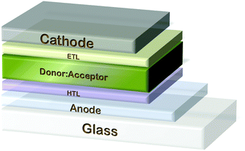
Organic photovoltaics (OPVs) based on conjugated polymers are of great interest due to the prospect of low cost and solution-based fabrication on top of flexible materials, offering important advantages over silicon technology. OPVs, which offer the benefit of low cost materials, high-throughput manufacturing methods and low energy expenditure,19 have attracted a lot of attention in the last 20 years as one of the most promising technologies. One subclass of these devices is based on the bulk heterojunction (BHJ) concept where a conjugated polymer (donor) and a fullerene (acceptor) are blended together in nanoscale morphology.20 These systems are by far the most deeply studied and reported21,22 since they enable efficient charge generation even in materials with very limited exciton diffusion length. Rapid progress in the research and the development of new polymer materials with a low bandgap and high charge carrier mobility has led to PCEs higher than 10%23,24 using one polymer as an absorber in both regular and inverted device structures.25–27 In a typical BHJ device the active layer is sandwiched between an anode and a cathode as outlined in Fig. 1. The solar radiation absorbed by the active medium leads to exciton generation. The excitons propagate to the acceptor/donor interface and split. The photogenerated carriers are collected in the respective electrode. Holes are transported to the anode while electrons are transported to the cathode. The anode typically consists of a substrate that is coated with a high work function transparent conducting electrode and modified with an interfacial hole selective/electron blocking layer between the electrode and the active layer. The ideal candidate material for an anode electrode should demonstrate high optical transparency and good charge transport properties. High transparency will assist more of the incident solar photons reach the active medium and good electrical conductivity allows the collection of highest number of photogenerated holes. The synergistic effect of these properties leads to the optimization of the OPV operational parameters. To this end, semi-transparent OPVs have attracted great attention e.g. due to their ‘smart’ applications in energy-harvesting windows.28,29 An important component in the OPVs is the transparent conductive electrode (TCE), the first layer of an OPV device that the incident solar electromagnetic radiation should transmit in order to be absorbed by the solar cell's active medium. High transparency will assist more of the incident solar photons reach the active medium and good electrical conductivity allows the collection of highest number of photogenerated holes. This will lead to the optimization of the OPV operational parameters (Jsc, PCE). Indium tin oxide (ITO) is the current state-of-the-art TCE material used. However, it faces a number of drawbacks including (a) high purchase cost and scarcity of indium reserves,30 (b) intrinsic brittleness property for flexible devices,31 (c) indium diffusion to the photoactive layers, which deteriorates device performance32 and (d) costly coating methods such as sputtering, evaporation, pulsed laser deposition and electroplating.31 It is clear that these issues highlight the need for ITO substitution with solution-processed materials that exhibit improved optoelectrical properties. Due to its exceptional properties graphene is highly attractive and is believed to be the next wonder material for optoelectronics, thus triggering its application as TCE in photovoltaic devices.
This mini review article focuses on the application of solution-processed rGO thin films as the anode TCE in OPV devices, replacing the traditional ITO. We summarize the studies on thermally, chemically and photochemically produced rGO, as well as on rGO composite TCE films. In addition, we review some promising routes for the rGO-based TCE treatment that enable the tuning of their opto-electrical properties and overcome the trade-off between the sheet resistance (Rs) and transmittance of the rGO TCEs. The application of graphene-based TCEs, replacing ITO, launches the era of lightweight, low cost, extended lifetime and more importantly flexible OPVs.
Applications of rGO-based TCEs in organic photovoltaics
A number of studies have investigated the application of rGO as the anode (positive electrode) in OPVs. OPV devices require a TCE with efficient carrier transport and thus high charge collection efficiency. The ideal TCE candidate material should exhibit high transparency (>80%), low sheet resistance (Rs < 100 Ω sq−1) and an appropriate work function (WF) (4.5–5.2 eV). In addition, the cost, including electrode preparation and compatibility with roll-to-roll (R2R) processes, must be considered. Despite the ideal optical (transparency >90%) and electrical (Rs ∼ 10–20 Ω sq−1) characteristics of ITO for its application as an electrode material and its favorable work function, the aforementioned drawbacks of ITO have intensified the research on graphene-based TCEs in OPVs. In this context, solution-processed rGO films exhibiting low electrical resistance, high transparency and a high work function must be developed.Thermally reduced GO TCEs in organic photovoltaics
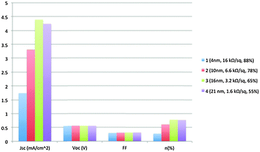
Yin et al.33 first proposed the application of solution-processed chemically reduced GO TCEs in OPV devices. In a typical process, GO solution was firstly spin-coated on the SiO2/Si substrate followed by thermal annealing at 1000 °C in the presence of Ar/H2 to remove the oxygen-containing groups and restore the conjugated structure of graphene. Subsequent coating of polymethyl methacrylate (PMMA) was used to provide an intermediate transfer substrate before the final transfer of rGO films onto polyethylene terephthalate (PET) substrates. The rGO-coated PET substrates were used as TCEs in flexible poly(3-hexylthiophene) (P3HT):phenyl-C61-butyric acid methyl ester (PC61BM)-based photovoltaic devices. Fig. 2 depicts the effect of the rGO electrode film thickness on the electrical characteristics of P3HT:PC61BM BHJ OPVs.Higher device performance dependence on the rGO film Rs was observed when the rGO films' optical transmittance exceeded 65%, while in lower optical transmittance (<65%), OPV's performance is dominated by the light transmission efficiency. It is worth mentioning that the OPV performance did not improve from device 3 to 4, revealing the optimum rGO thickness for OPV performance. The power conversion efficiency (PCE) of device 3 reached 0.78%, which is slightly lower than the PCE value reported for CVD-graphene/PET based OPV devices (1.18%).34 This is attributed to the lower Rs of the CVD grown graphene compared to the chemically derived rGO film.
The flexibility of the rGO films was also investigated (Fig. 3). BHJ OPV electrical properties incorporating rGO films as electrodes demonstrated excellent tolerance under high bending conditions and multiple number of bending cycles. The threshold point beyond which OPV devices with rGO/PET films demonstrated degradation due to bending depends on the rGO film thickness. Yin et al.33 demonstrated that OPV devices subjected to tensile stress exhibited stable performance when the rGO electrode was relatively thick. The authors confirmed that the noticed electrical degradation of rGO-based OPVs after various bending cycles was related to an observed increase of rGO/PET Rs. Electrical measurements showed that the rGO/PET electrode Rs increased from 16 to 18 kΩ sq−1 and 3.2 to 3.5 kΩ sq−1, respectively, for the 4 and 16 nm thick rGO films after 1600 bending cycles.
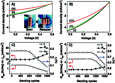 | ||
| Fig. 3 Current density–voltage (J–V) curves of (A) device 1 after applying (i) 400, (ii) 800 and (iii) 1200 cycles of bending and (B) device 3 after applying (I) 800, (II) 1200 and (III) 1600 cycles of bending. Panels C and D demonstrate the short circuit current density, overall power conversion efficiency (n) and sheet resistance RSR for devices 1 and 3 respectively as a function of the number of bending cycles.33 | ||
Geng et al.35 reported a simple method for preparing graphene TCEs using a chemically converted graphene (CCG) suspension obtained via controlled chemical reduction of exfoliated GO in the absence of dispersants. Upon thermal annealing for 15 min at three different temperatures (200, 400 and 800 °C) under vacuum in a furnace tube, the recovery of sp2 carbon networks of the graphene sheets was achieved, with the resulting CCG films exhibiting an Rs of the order of 103 Ω sq−1 at 50% transparency (at 550 nm). Each thermally annealed CCG film demonstrated lower Rs than the thermally annealed GO as depicted in Fig. 4b. This is due to the apparently greater extent of sp2 carbon networks restoration during the two-step reduction of the CCG films. The transparency of the CCG films decreases linearly with respect to the volume of the CCG suspension used to prepare the vacuum-filtered film (Fig. 4c). By increasing the annealing temperature, the transparency of the CCG films decreased due to thermal improvement of the sp2 carbon networks in the CCG sheets.
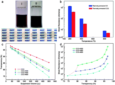 | ||
| Fig. 4 (a) A 0.1 mg mL−1 GO suspension (I), the resultant CCG suspension (II), and the CCG films prepared using 160, 240, 320, 400, 480 and 560 μL of a 10 mg L−1 CCG suspension. (b) Comparison of the sheet resistance of the GO and CCG films annealed at 200, 400 and 800 °C. (c) Changes in the transparency of CCG, CCG-A200, CCG-A400, and CCG-A800 films as a function of the volume (μL) of the 10 mg L−1 CCG suspension used for film preparation and (d) sheet resistance values of CCG-A200, CCG-A400, and CCG-A800 films as a function of film transparency.35 | ||
In Fig. 4d the lowering of the Rs, as the annealing temperature increases, is attributed to the smaller induced distance due to the removal of the functional groups between the layers of CCG sheets, which facilitates charge carrier transport across the CCG sheets. The annealing temperatures reduce the interlayer distance in CCG-A800 films to 0.354 nm, approaching the value of bulk graphite. As the transparency decreased from this point, the Rs decreased linearly to the order of 103 Ω sq−1, indicating that reduction occurred effectively and uniformly from the outermost to the inner layers.35
The induced structural changes in the CCG due to thermal reduction led to the film conductivity improvement since (a) the restoration of the sp2 carbon networks was critical for increasing the charge carrier transport in individual CCG layers and (b) the interlayer distance was reduced to a level close to the value of bulk graphite, thereby improving the charge carrier transport across the CCG layers. As a proof of concept, CCG films were used as TCEs in P3HT:PC61BM-based OPV devices yielding a PCE of 1.01%, approximately half of the PCE value in ITO-based devices (Fig. 5).
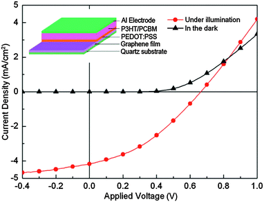 | ||
| Fig. 5 J–V curves for P3HT:PC61BM-based OPV devices incorporating the CCG-A800 film as a TCE. The inset shows the architecture of the solar cell device.35 | ||
Chemically reduced GO TCEs in organic photovoltaics
Wu et al.36 compared the electrical properties of rGO films prepared by following two different reduction methods, chemical and thermal treatment. Using GO prepared by Hummers' method as pristine materials, the group investigated the conductivity properties of GO reduced by vacuum annealing at 1100 °C and by a combination of hydrazine treatment and Ar annealing at 400 °C. The results demonstrated that the vacuum annealing reduction resulted in rGO films with slightly better transparency and conductivity compared to the films reduced using the combination of chemical and thermal treatment. In both cases, the film surfaces were free from spikes that can cause short circuit in optoelectronic devices. This is an advantage of graphene-based electrodes over carbon nanotube or metal nanowire mesh electrodes which require a thick, spin coated polymer buffer layer in order to prevent shorts, generated by surface spikes. Fig. 6 depicts the transmittance and Rs with respect to the rGO film thickness with the two different fabrication methods. In general, for <20 nm film thickness, the optical transmittance was >80%, while the Rs varied from 5 kΩ sq−1 to 1 MΩ sq−1. Bilayer small molecule OPV cells were fabricated on rGO/glass substrates. The fabricated cells using copper phthalocyanine (CuPc)/fullerene (C60) as an active layer demonstrated a PCE of ∼0.4%, in contrast to ITO-based devices which exhibited a PCE of ∼0.84%. The higher Rs of graphene-based electrodes compared to the ITO electrodes was the reason for the observed PCE difference.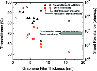 | ||
| Fig. 6 Transmittance at λ = 550 nm (triangles) and sheet resistance (circles) as a function of the graphene film thickness for both reduction methods: vacuum annealing at 1100 °C (open symbols) and hydrazine treatment and argon annealing at 400 °C (filled symbols).36 | ||
Recently, Moaven et al.37 reported the synthesis of a rGO/Ag nanocomposite electrode suitable for OPV devices. The reported technique is applicable to flexible substrates. The optical and electrical properties were determined by altering the Ag concentration of the nanocomposite and the electrode thickness. Flexible electrodes with Rs as low as 83 kΩ sq−1 and with a transmittance of 47% were achieved. The highest PCE of the fabricated organic photovoltaic device based on a rGO/Ag was 0.18%.
In another study, Huang et al.38 prepared highly conductive and transparent graphene-based electrodes with tunable work functions by combining single walled carbon nanotubes (SWCNTs) with chemically reduced GO. Through doping with alkali carbonates, the work function of solution processed rGO-SWCNTs was properly modulated to match the lowest unoccupied molecular orbital (LUMO) of PC61BM, leading to lower ohmic contact with the active layer which enhances the charge injection and thereby improves device performance. In addition, SWCNTs in the hybrid system of rGO-SWCNT operate as conductive percolation paths that short circuit the rGO sheets. To demonstrate the applicability of doping-effect to the work function tuning of rGO-SWCNT, lower work function electrodes were used as cathodes in inverted architecture polymer photovoltaic devices (Fig. 7). The devices based on P3HT:PC61BM exhibited a maximum PCE of 1.27% and excellent flexibility even under bending angles of more than 60°.
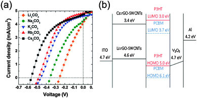 | ||
| Fig. 7 (a) J–V characteristics of the inverted P3HT:PC61BM-based devices incorporating rGO-SWCNT doped with various alkali carbonates as the cathode. (b) Energy level diagrams of inverted solar cells featuring alkali carbonate-doped carbon-based cathodes.38 | ||
Photochemically reduced GO TCEs in organic photovoltaics
Kymakis et al.39 presented for the first time a facile, laser-based technique to reduce GO films on top of flexible substrates. The experimental setup is depicted in Fig. 8a and it consisted of (1) a Ti:Sapphire pulsed laser source, (2) a 10 mm diameter lens and (3) a high precision X–Y computer controlled translation stage on top of which the film was placed and translated across the focused laser beam.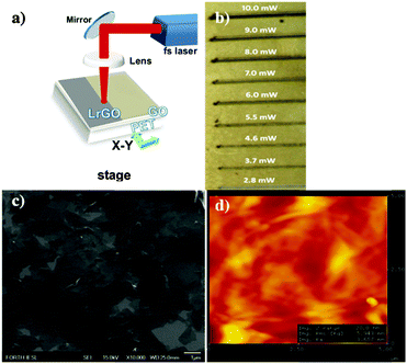 | ||
| Fig. 8 (a) Laser-based GO reduction experimental setup. (b) Scan lines obtained upon irradiation with 100 fs pulses at different fluences indicating the gradual color change due to reduction. (c) SEM and (d) AFM images of LrGO films on PET.39 | ||
During the reduction process the fs laser beam irradiated the as-spun GO layers, while it was translated across the layers. The reduction of GO can be optically noticed. Fig. 8b displays scan lines obtained upon irradiation with 100 fs pulses at different fluencies indicating the gradual color change due to the reduction. The yellowish color of the pristine film was gradually turned into black indicating that GO is rapidly reduced via the laser treatment in air, without the use of any reducing chemical agent. Scanning electron microscopy (SEM) and atomic force microscopy (AFM) analysis demonstrated that no or minor ablation effects occur during the reduction process (Fig. 8c and d).
One of the motivations towards the use of solution-cast laser reduced GO (LrGO) electrodes is to realize highly flexible OPVs that can be used for compact roll-type solar modules. In this context, the LrGO films were used to fabricate flexible OPV devices (Fig. 9a and b) in order to determine their photovoltaic characteristics and identify the combination of transparency and Rs that provides the best performance. Compared to the thermally reduced GO-based OPV devices (PCE ∼ 0.78%),33 LrGO-based OPVs presented an efficiency enhancement of 41%, obtained with a 16.4 nm thick film having an Rs of 1.6 kΩ sq−1 and transparency of 70%. It is evident that the LrGO film is responsible for the higher efficiency, indicating the superiority of the laser ablation method, compared with the chemical method.
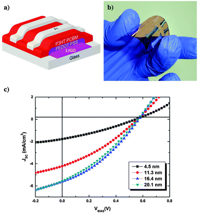 | ||
| Fig. 9 (a) Schematic and (b) picture of the flexible PET/rGO/PEDOT:PSS/P3HT:PC61BM/Al photovoltaic devices fabricated and (c) the illuminated current density–voltage (J–V) curves of the solar cells with various LrGO film thicknesses.39 | ||
The demonstrated low performance of rGO TCEs in terms of conductivity and transmittance (Rs ∼ 1 kΩ sq−1, 70% transmittance) compared to the ITO TCEs (Rs ∼ 15 Ω sq−1, 90% transmittance) has triggered new efforts to improve graphene-based TCE performances. One of the most interesting strategies for increasing the transparency of a TCE material while keeping its conductivity almost unaffected is the employment of a mesh structure with periodic lines.40 OPV devices incorporating graphene mesh electrodes have demonstrated performances comparable to those using ITO electrodes.41,42 By varying the grid width, spacing and thickness, it is possible to control the Rs and transparency of the films.43
Zhang et al.44 reported the preparation of graphene mesh electrodes (GMEs) by using the standard industrial photolithography and O2 plasma etching process (Fig. 10). The transparency and the Rs of the graphene electrodes before the mask-based etching were ∼8% and 150 Ω sq−1. After the etching technique, the electrodes transparency and Rs were measured to be 65% and 750 Ω sq−1, respectively. The GME transparency was directly defined by the mesh (a) pit depth and (b) period whereas its conductance was defined mainly by the mesh (a) pit depth and (b) linewidth. The pit depth was controlled by the duration of the O2 process, with 4–10 min of O2 plasma etching time required for high transparent mesh pits. OPV devices employing optimum pit depth GMEs based on the P3HT:PC61BM active layer have been fabricated, demonstrating a PCE equal to 2.04%.
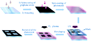 | ||
| Fig. 10 Illustration of the fabrication steps for the preparation of GMEs.44 | ||
Konios et al.45 presented a different method using a laser beam to directly pattern a mesh on the surface of rGO films deposited onto flexible substrates, avoiding in this way the use of complicated photolithographic,46 ion beam,47 chemical etching,48 template49 and O2 plasma techniques.50 The absence of a TEM grid patterning mask,51 and the lack of any transfer step, makes the proposed technique a one-step method. In addition, there is no use of any photo-resistive material52 or pre-patterned elastomeric stamps,53 while the use of fs laser pulses allows the patterning of micro size holes on top of any flexible low cost material. The mesh patterning can be accurately controlled in order to significantly enhance the electrode transparency with a small increase in the Rs and therefore appropriately handles the existing trade-off between transparency and electrical conductivity. The optoelectrical properties of rGO thin films were found to be directly dependent on the interplay between the periodicity and the geometrical characteristics of the mesh pattern structure. Fig. 11 illustrates the rGO mesh electrode preparation setup and SEM images of the laser induced patterns respectively. The attractiveness of the proposed technique is that it permits fine-tuning via variation of the irradiation dose (energy, number of pulses) and/or the periodicity and thus the neck width of the mesh. Although the initial transmittance of the rGO layer was ∼20%, it was significantly improved to ∼85% after the laser treatment. As a proof of the feasibility and the efficiency of the proposed laser patterning technique, flexible devices based on poly[N-9′-heptadecanyl-2,7-carbazole-alt-5,5-(4′,7′-di-2-thienyl 2′,1′,3′-benzothiadiazole)] (PCDTBT):[6,6]-phenyl C71 butyric acid methyl ester (PC71BM) photoactive blends deposited on reduced GO micromesh (rGOMM) were fabricated and compared with those deposited on ITO (Fig. 12a and b).
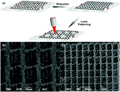 | ||
| Fig. 11 (a) Illustration of the laser induced patterns on the rGO films and (b and c) SEM images of the laser induced patterns: the darker spots correspond to the laser processed areas where the mesh lines correspond to the lighter colored paths.45 | ||
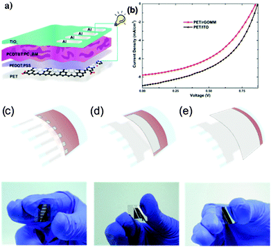 | ||
| Fig. 12 (a) Schematic illustration of the BHJ OPV device with the laser-induced rGOMM as TCE. (b) The illuminated current density–voltage (J–V) curves of the solar cells with rGOMM (red) and ITO (black) as TCE. Schematic illustration and photographs of different active area devices tested: (c) 4 mm2, (d) 50 mm2 and (e) 135 mm2.45 | ||
The optimum photovoltaic parameters for the rGOMM-based devices were extracted for transparency ∼59.1% and Rs ∼ 565 Ω sq−1, with the resulting PCE of 3.05%, the highest reported so far for flexible OPV devices incorporating solution-processed graphene-based electrodes. Another important issue studied in this work was the determination of the effectiveness of the proposed method when tested in large area photovoltaic cells (Fig. 12c–e). This is crucial for the future development of this technology by upscaling from lab solar cells to solar modules. The results showed that the deterioration in the photovoltaic performance of both rGOMM and ITO electrodes tested was almost the same (for a 135 mm2 active area, it was 63.2% of the initial PCE for ITO and 64.9% for rGOMM respectively). Therefore, the proposed method can be effectively applied when upscaling to large area photovoltaic cells or solar modules without compromising the photovoltaic efficiency compared with the widely commercialized ITO transparent electrode.
The intensive research effort in the field of solution-processed graphene-based TCEs, during the last five years, is demonstrated in Fig. 13, while a summary of the optoelectrical properties of graphene-based TCEs in OPV devices is presented in Table 1. Recent research progress by a number of groups has resulted in the increase of the PCE of OPV devices incorporating graphene-based TCEs from 0.13% to 3.7% for rigid devices. In addition, the progress on the flexible graphene-based devices was also incredible with an efficiency enhancement from 0.78% to 3.05%.
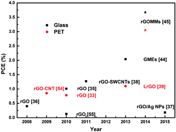 | ||
| Fig. 13 OPV performance of solution processed graphene-based TCEs with different active layers extracted from the literature.33,35–39,44,45,54,55 Black squares stand for rigid devices, while red circles stand for devices on flexible substrates. Stars illustrate the champion PCE achieved.45 | ||
Conclusions and perspectives
In this minireview paper, the feasibility of solution-processed graphene-based films as anode electrodes in OPVs has been presented. (a) Chemically converted graphene, (b) thermally and photochemically reduced graphene oxide, (c) composite reduced graphene oxide-carbon nanotubes and (d) reduced graphene oxide mesh films have demonstrated their applicability in OPV cells as transparent, conductive electrodes. The successful large scale application of such schemes poses a significant engineering challenge and ongoing effort for high performance printed optoelectronic devices such as flexible OPVs. Despite the advantages offered by graphene-based materials regarding the manufacturing and purchase cost, compatibility with flexible materials, work function tuning (by controlling graphene size and layer structure and through functionalization), transparency and solubility, significant improvement is needed in order to match the corresponding properties of ITO films. Although the current performance of graphene-based electrode OPVs is lower than that of ITO, there is plenty of room for improvement and study of OPVs employing graphene as an anode electrode.Future work should be focused on (a) cost-effective approaches for large-scale production of graphene or reduced graphene oxide, (b) improving the effectiveness of graphene oxide reduction methods, (c) enhancing film conductivity without disrupting its transmittance and (d) improving the graphene-based film morphology. Towards improving TCE conductivity, graphene based electrodes incorporating metal nanoparticles (e.g. Au) with different sizes and shapes may enable the production of graphene–NP electrodes with even lower resistance and high mechanical stability. In addition, hybrid films of reduced graphene oxide and 1D conductive bridging materials, such as metal nanowires which present better mechanical properties than ITO films, can significantly reduce the overall resistance of the films. The electric pathways provided by the metal nanowire bridges among the graphene layers can enhance the conductivity, without sacrificing their optical properties, leading to improved performance of graphene-based TCEs. The incorporation of metal-graphene based TCEs into optoelectronic devices demonstrates their potential for ITO replacement in a broad range of applications including large-area flexible displays, photovoltaics, and organic light-emitting diodes.
Acknowledgements
The research leading to these results has received funding from the European Union Seventh Framework Programme under Grant Agreement No. 604391 Graphene Flagship.Notes and references
- Q. Cao, H. S. Kim, N. Pimparkar, J. P. Kulkarni, C. Wang, M. Shim, K. Roy, M. A. Alam and J. A. Rogers, Nature, 2008, 454, 495 CrossRef CAS PubMed.
- M. Singh, H. M. Haverinen, P. Dhagat and G. E. Jabbour, Adv. Mater., 2010, 22, 673 CrossRef CAS PubMed.
- F. Torrisi, T. Hassan, W. Wu, Z. Sun, A. Lombardo, T. S. Kulmala, G. Hsieh, S. Jung, F. Bonaccorso, P. J. Paul, V. Chu and A. C. Ferrari, ACS Nano, 2012, 6, 2992 CrossRef CAS PubMed.
- E. Kymakis, C. Petridis, T. D. Anthopoulos and E. Stratakis, IEEE, 2014, 20, 6573325 Search PubMed.
- G. Kakavelakis, D. Konios, E. Stratakis and E. Kymakis, Chem. Mater., 2014, 26, 5988 CrossRef CAS.
- E. Stratakis, K. Savva, D. Konios, C. Petridis and E. Kymakis, Nanoscale, 2014, 6, 6925 RSC.
- M. M. Stylianakis, M. Sygletou, K. Savva, G. Kakavelakis, E. Kymakis and E. Stratakis, Adv. Opt. Mater., 2015, 3, 658 CrossRef CAS.
- K. S. Novoselov, A. K. Geim, S. V. Morozov, D. Jiang, Y. Zhang, S. V. Dubonos, I. V. Grigorieva and A. A. Firsov, Science, 2004, 306, 666 CrossRef CAS PubMed.
- N. Behabtu, J. R. Lomeda, M. J. Green, A. L. Higginbotham, A. Sinitskii, D. V. Kosynkin, D. Tsentalovich, A. N. G. Parra-Vasquez, J. Schmidt, E. Kesselman, Y. Cohen, Y. Talmon, J. M. Tour and M. Pasquali, Nat. Nanotechnol., 2010, 5, 406 CrossRef CAS PubMed.
- K. S. Kim, Y. Zhao, H. Jang, S. Y. Lee, J. M. Kim, K. S. Kim, J.-H. Ahn, P. Kim, J.-Y. Choi and B. H. Hong, Nature, 2009, 457, 706 CrossRef CAS PubMed.
- M. Choucair, P. Thordason and J. A. Stride, Nat. Nanotechnol., 2009, 4, 30 CrossRef CAS PubMed.
- X. Wang, L. Zhi, N. Tsao, Z. Tomori, J. Li and K. Mullen, Angew. Chem., Int. Ed., 2008, 47, 2990 CrossRef CAS PubMed.
- C. Berger, Z. Song, T. Li, A. Y. Orbazghi, R. Feng, Z. Dai, A. N. Marchenkov, E. H. Conrad, P. N. First and W. A. De Heer, J. Phys. Chem. B, 2004, 108, 19912 CrossRef CAS.
- N. Zhuang, C. Liu, L. Jia, L. Wei, J. Cai, Y. Guo, Y. Zhang, X. Hu, J. Chen, X. Chen and Y. Tang, Nanotechnology, 2013, 24, 325604 CrossRef PubMed.
- D. Konios, M. M. Stylianakis, E. Stratakis and E. Kymakis, J. Colloid Interface Sci., 2014, 430, 108 CrossRef CAS PubMed.
- S. Stankovich, D. A. Dikin, R. D. Piner, K. A. Kohlhaas, A. Kleinhammes, Y. Jia, Y. Wu, S. T. Nguyen and R. S. Ruoff, Carbon, 2007, 45, 1558 CrossRef CAS.
- C. Mattevi, G. Eda, S. Agnoli, S. Miller, K. A. Mikhoyan, O. Celik, D. Matsrogiovanni, G. Granozzi, E. Garfunkel and M. Chhowalla, Adv. Funct. Mater., 2009, 19, 2577 CrossRef CAS.
- R. Y. N. Gengler, D. S. Badali, D. Zhang, K. Dimos, K. Spyrou, D. Gournis and R. J. D. Miller, Nat. Commun., 2013, 4, 2560 Search PubMed.
- F. C. Krebs, T. Tromholt and M. Jørgensen, Nanoscale, 2010, 2, 873 RSC.
- C. J. Brabec, M. Heeney, I. McCulloch and J. Nelson, Chem. Soc. Rev., 2011, 40, 1185 RSC.
- Y.-J. Cheng, S.-H. Yang and C.-S. Hsu, Chem. Rev., 2009, 109, 5868 CrossRef CAS PubMed.
- A. Mishra and P. Bäuerle, Angew. Chem., Int. Ed., 2012, 51, 2020 CrossRef CAS PubMed.
- M. C. Schraber and N. S. Sariciftci, Prog. Polym. Sci., 2013, 38, 1929 CrossRef PubMed.
- C.-C. Chen, W.-H. Chang, K. Yoshimura, K. Ohya, J. You, J. Gao, Z. Hong and Y. Yang, Adv. Mater., 2014, 26, 5670 CrossRef CAS PubMed.
- X. Guo, N. Zhou, S. J. Lou, J. Smith, D. B. Tice, J. W. Hennek, R. P. Ortiz, J. T. L. Navarrete, S. Li, J. Strzalka, L. X. Chen, R. P. H. Chang, A. Facchetti and T. J. Marks, Nat. Photonics, 2013, 7, 825 CrossRef CAS.
- Z. He, C. Zhong, S. Su, M. Xu, H. Wu and Y. Cao, Nat. Photonics, 2012, 6, 591 Search PubMed.
- Z. He, B. Xiao, F. Liu, H. Wu, Y. Yang, S. Xiao, C. Wang, T. P. Russell and Y. Cao, Nat. Photonics, 2015, 9, 174 CrossRef CAS.
- G. Li, C. W. Chu, V. Shrotriya, J. Huang and Y. Yang, Appl. Phys. Lett., 2006, 88, 253503 CrossRef.
- W. Yu, L. Shen, Y. Long, W. Guo, F. Meng, S. Ruan, X. Jia, H. Ma and W. Chen, Appl. Phys. Lett., 2012, 101, 153307 CrossRef.
- Y. H. Kim, S. Schubert, R. Timmreck, L. M. Meskamp and K. Leo, Adv. Energy Mater., 2013, 3, 1551 CrossRef CAS.
- Y. Galagan, E. W. C. Coenen, B. Zimmermann, L. H. Sloof, W. J. H. Verhees, S. C. Veenstra, J. M. Kronn, M. Jorgensen, F. C. Krebs and R. Andriessen, Adv. Energy Mater., 2014, 4, 1300498 CrossRef.
- W. J. Da Silva, H. P. Kim, A. R. Yusoff and J. Jang, Nanoscale, 2013, 5, 9324 RSC.
- Z. Yin, S. Sun, T. Salim, S. Wu, X. Huang, Q. He, Y. M. Lam and H. Zhang, ACS Nano, 2010, 4, 5263 CrossRef CAS PubMed.
- L. G. D. Arco, Y. Zhang, C. W. Schlenker, K. Ryu, M. E. Thomson and C. Zhou, ACS Nano, 2010, 4, 2865 CrossRef PubMed.
- J. Geng, L. Liu, S. B. Yang, S. C. Youn, D. W. Kim, J. S. Lee, J. K. Choi and H. T. Jung, J. Phys. Chem. C, 2010, 114, 14433 CAS.
- J. Wu, H. Becerril, Z. Bao, Z. Liu, Y. Chen and P. Peumans, Appl. Phys. Lett., 2008, 92, 263302 CrossRef.
- S. Moaven, L. Naji, F. A. Taromi and F. Sharif, RSC Adv., 2015, 5, 30889 RSC.
- J. H. Huang, J. H. Fang, C. C. Liu and C. W. Chu, ACS Nano, 2011, 5, 6262 CrossRef CAS PubMed.
- E. Kymakis, K. Savva, M. M. Stylianakis, C. Fotakis and E. Stratakis, Adv. Funct. Mater., 2013, 23, 2742 CrossRef CAS.
- H. Wu, L. Hu, M. W. Rowell, D. Kong, J. J. Cha, J. R. McDonough, J. Zhu, Y. Yang, M. D. McGehee and Y. Cui, Nano Lett., 2010, 10, 4242 CrossRef CAS PubMed.
- M. G. Kang, M. S. Kim, J. Kim and L. Cuo, Adv. Mater., 2008, 20, 4408 CrossRef CAS.
- L. Yang, T. Zhang, H. Zhou, S. Price, B. J. Wiley and W. You, ACS Appl. Mater. Interfaces, 2011, 3, 4075 CAS.
- J. Zou, H. L. Yip, S. K. Hau and A. K. Y. Jen, Appl. Phys. Lett., 2010, 96, 203301 CrossRef.
- Q. Zhang, X. Wan, F. Xing, L. Huang, G. Long, N. Yi, W. Ni, Z. Liu, J. Tian and Y. Chen, Nano Res., 2013, 6, 478 CrossRef CAS.
- D. Konios, C. Petridis, G. Kakavelakis, M. Sygletou, K. Savva, E. Stratakis and E. Kymakis, Adv. Funct. Mater., 2015, 25, 2213 CrossRef CAS.
- J. Bai, X. Zhong, S. Jiang, Y. Huang and X. Duan, Nat. Nanotechnol., 2010, 5, 190 CrossRef CAS PubMed.
- N. E. Sosa, J. Liu, C. Chen, T. J. Marks and M. C. Hersam, Adv. Mater., 2009, 21, 721 CrossRef CAS.
- Y. Zhu, S. Murali, M. D. Stoller, K. J. Ganesh, W. Cai, P. J. Ferreira, A. Pirkle, R. M. Wallace, K. A. Cychosz, M. Thommes, D. Su, E. A. Stach and R. S. Ruoff, Science, 2011, 332, 1537 CrossRef CAS PubMed.
- Z. L. Wang, D. Xu, H. G. Wang, Z. Wu and X. B. Zhang, ACS Nano, 2013, 7, 2422 CrossRef CAS PubMed.
- Q. Zhang, X. Wan, F. Xing, L. Huang, G. Long, N. Yi, W. Ni, Z. Liu, J. Tian and Y. Chen, Nano Res., 2013, 6, 478 CrossRef CAS.
- J. S. Oh, S. H. Kim, T. Hwang, H.-Y. Kwon, T. H. Lee, A. H. Bae, H. R. Choi and J. D. Nam, J. Phys. Chem. C, 2013, 113, 663 Search PubMed.
- Y.-Q. Bie, Y.-B. Zhou, Z.-M. Liao, K. Yan, S. Liu, Q. Zhao, S. Kumar, H.-C. Wu, G. S. Duesberg, G. L. W. Cross, J. Xu, H. Peng, Z. Liu and D.-P. Yu, Adv. Mater., 2011, 23, 3938 CrossRef CAS PubMed.
- Q. He, H. G. Sudibya, Z. Yin, S. Wu, H. Li, F. Boey, W. Huang, P. Chen and H. Zhang, ACS Nano, 2010, 4, 3201 CrossRef CAS PubMed.
- V. C. Tung, L. M. Chen, M. J. Allen, J. K. Wassei, K. Nelson, R. B. Kaner and Y. Yang, Nano Lett., 2009, 9, 1949 CrossRef CAS PubMed.
- Y. Xu, G. Long, L. Huang, Y. Huang, X. Wan, Y. Ma and Y. Chen, Carbon, 2010, 48, 3308 CrossRef CAS.
| This journal is © The Royal Society of Chemistry 2016 |

