
Electrical gas sensors based on structured organic ultra-thin films and nanocrystals on solid state substrates
Lizhen
Huang
,
Zi
Wang
,
Xiaofei
Zhu
and
Lifeng
Chi
*
Institute of Functional Nano & Soft Materials (FUNSOM), Jiangsu Key Laboratory for Carbon-Based Functional Materials & Devices, Soochow University, Suzhou, 215123, P. R. China. E-mail: chilf@suda.edu.cn
First published on 10th May 2016
Abstract
Gas sensors, as useful tools to detect specific gas species such as toxic and explosive gases or volatile organic compounds, are the key components for environmental monitoring, fruit maturity and food safety monitoring, health care, and so on. The present commercial products based on porous metal oxide materials still face problems, such as high temperature operation and low level of selectivity. Thin films or nanostructures of organic materials with thickness or grain size down to nanometer scale represent promising candidates for gas sensing due to their potential for achieving high selectivity, portability and low cost. However, there are still challenges related to their stability, reproducibility and response/recovery speed despite the efforts in materials design, morphology control or device configuration, all of which have been expended during the last few decades. In this review, we summarize the progress of recent research on gas sensors based on organic ultra-thin films and nanostructures. We specifically discuss the effect of microstructure in the active layer on the sensing performance and mechanism.
1. Introduction
Gas sensors that can detect certain gas species, such as H2S, NO2, NH3, CO2 and volatile organic compounds (VOCs), in different environments are critical elements in many fields, such as environmental monitoring, fruit maturity and food safety monitoring, health care, security and industrial process control.1 Based on the variable properties of gas sensors used for detection, these sensors are classified into several types, such as electrical, optical or acoustic sensors.1–3 Among them, electrical sensors are the most popular because of their portable nature and low cost. Commercial products are mainly based on metal oxide materials with porous microstructure.4 The limitations of such gas sensors are their relatively slow response and recovery process, lack of selectivity and high working temperature. Therefore, many potential substitutes have been developed aiming for low-cost, room-temperature-operated high performance gas sensors.Organic semiconductors, as one of the most promising candidates for gas sensing, have attracted extensive attention in expectation of achieving good selectivity, portability and low cost.5–8 However, their shortcoming with respect to charge transport to some extent limits their sensitivity and response/recovery speed. The microstructure of the active layer has proved to be a key factor for achieving high sensitivity and fast response/recovery.9–13 Traditional thick films or bulk materials usually impose a significant barrier for gas diffusion and charge transport, which results in slow response and poor recovery. In recent years, many groups have dedicated their efforts for controlling film thickness and texture to realize a structured active layer with a large surface-to-volume ratio and an efficient gas absorption/diffusion and charge transport path. Ultra-thin, low-dimensional structured films and nanostructures have therefore become hot topics in the field,14–21 especially nanomaterials such as carbon nanotubes, nanowires or nanoparticles, which have been discussed in several reviews.22–25
In this review, we will summarize recent studies on electrical gas sensors based on a structured active layer of organic materials, such as ultra-thin organic films, organic nanocrystals or organic decorated nanostructures, and discuss the influence of texture on the sensing performance and mechanism. Different from the prior reviews, this review mainly concentrates on the organic layer and discusses the role of organic materials in the electrical gas sensors. The first part will address the ultra-thin organic films with a single component, followed by a section focused on organic films with multiple components. Section 4 will concentrate on the nanocrystals of organic compounds, and Section 5 will focus on inorganic nanostructures decorated with organic molecular layers. Finally, we will discuss the effect of texture on the sensing performance and mechanism.
In advance, we will briefly introduce the principle of electrical gas sensors. There are two types of electrical gas sensors, resistor or transistor type (Fig. 1a). The organic semiconductor-involved gas sensors normally use the organic semiconductor as the active material and the sensing layer. The imposed or exposed gaseous analytes will interact with the active layer, which will then lead to the variation of carrier density or charge trap in the devices. Such variation will be reflected by the measured conductivity, mobility or threshold voltage variation, as shown in Fig. 1b. Different concentrations of analytes will mutually result in the variation of the measured electrical signals. In addition to the magnitude of variation (sensitivity), the speed of response and recovery, as well as the selectivity are the critical parameters to evaluate the performance of a sensor.
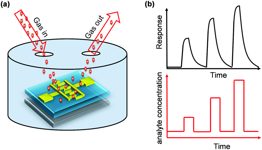 | ||
| Fig. 1 (a) Schematic diagram of a gas sensor configuration and (b) the measured signal in response to exposure to periodic pulses of analyte gas. | ||
2. Organic ultra-thin films
In the early stages of gas sensor development when organic materials were applied to the design of solid-state gas sensors, dense and thick films were used to maintain a detectable signal and to increase gas absorption.9,10,26 These early devices had a very slow recovery speed. This became a vital issue, and thus thermal annealing or UV-light was commonly needed to speed up the recovery time, complicating the fabrication process and increasing the cost. Furthermore, the organic semiconductor active layer undergoes a morphological or structural change during annealing, leading to unreliable performance. One easy way to solve the problem is to reduce the thickness of the active layer. This could shorten the diffusion time for analyte molecules, especially for transistor type devices where the effective conducting channel is mainly located in the first few layers. A. C. Kummel et al. fabricated an ultra-thin cobalt phthalocyanine (CoPc) transistor gas sensor with a 4 ML (ML = monolayer) film as the active layer.14 Although the transistor performance of a 4 ML device is not as good as that of a 50 ML device, the response to several organic vapours, such as ethyl acetate (EA), toluene (TE), diisopropyl methylphosphonate (DIMP), nitrobenzene (NB), and methanol (MeOH), is much better than that of the 50 ML device, especially with regard to the response and recovery speed (Fig. 2). Similarly, H. W. Katz et al. reported sensors with fast response and high sensitivity based on ultra-thin films regardless of whether they were fabricated from a vacuum deposition or solution process.15,27 Since decreased film thickness may reduce the conductivity, the film quality of these ultra-thin films is more crucial and requires a high level of ordering to maintain a detectable signal. Recently, D. Zhu et al. fabricated an ultra-thin organic film by spin-coating which presented a nearly layer-by-layer growth from the initial stage.28 These as-prepared gas sensors could display faster response and higher sensitivity to NH3 compared with thick films, which should relate to the high charge-carrier mobility.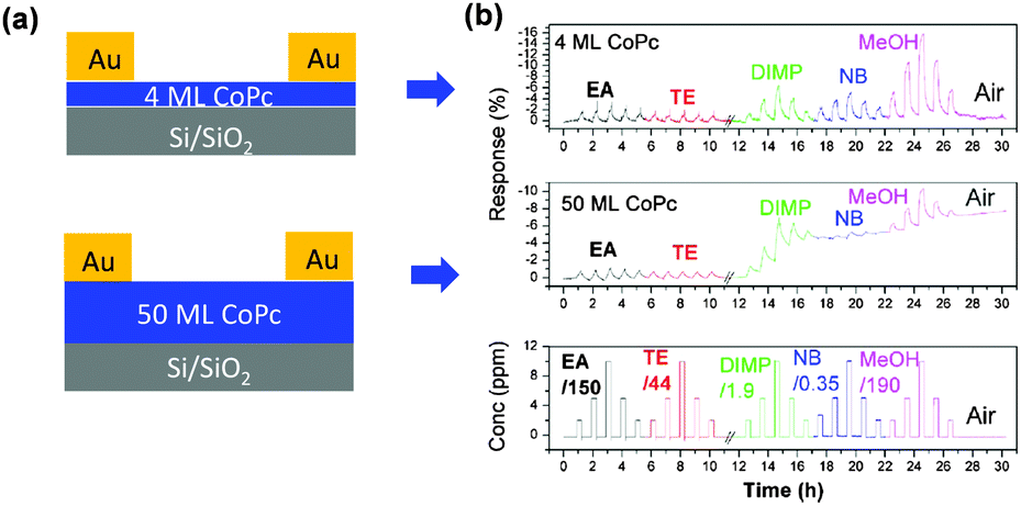 | ||
| Fig. 2 (a) Configurations of transistor gas sensors with different thicknesses of the active layer; (b) the response intensity of the corresponding transistor gas sensors on exposure to different analytes with varied concentrations. Reproduced with permission from ref. 14. | ||
The improvement in sensing was also observed for chemiresistor type sensors based on ultra-thin films with a highly ordered nature. D. Yan et al. reported chemiresistor type gas sensors based on ultra-thin vanadyl phthalocyanine (VOPc) films (1–2 ML) fabricated using a weak epitaxy growth method.29 The resulting highly ordered terraced-like film shows a response variation of 50% to 1 ppm NO2 at room temperature. Although this device still suffers from the slow recovery issue, it performs much better than the polycrystalline films that are directly grown on amorphous substrates.
Besides the improvement of molecular ordering in ultra-thin films, modulation of the film texture is also effective for achieving high performance gas sensors. L. Chi et al. fabricated structured ultra-thin films of dialkyl tetrathiapentacene by fast dip-coating for sensing NH3 (Fig. 3a).30 This structured film consists of ultra-thin, one-dimensional continuous microstripe crystals that possess an efficient charge transport path through the long stripe crystals and provide a fast absorption/diffusion path for analyte gas through the surface and intervals between microstripes, as illustrated in Fig. 3b–d. A very fast response/recovery speed with high sensitivity was achieved based on the transistor type sensors (Fig. 3e–h). The response time is 27–36 s and the recovery time is 10 s with gas sensitivity up to two orders of magnitude to NH3. In contrast, for a non-structured continuous film, the response/recovery time needed is 70–130 s, with a low sensitivity of 10. The sensing mechanism of this sensor, as explained by the authors, depends on the increased trap density caused by exposure to NH3, wherein the trap originates from the de-doping effect and dipole–charge interaction between NH3 and the acene derivatives.31,32
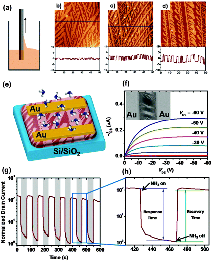 | ||
| Fig. 3 (a) Schematic diagram of the dip-coating process; (b–d) AFM height images of the dip-coating films with different pulling speeds; (e) configuration of the transistor gas sensor based on this structured film; (f) the output characteristics of the transistor, inset: SEM image of the real device; (g) the drain current evolution with periodic pulses on exposure to NH3; (h) magnified view of (g). Reproduced with permission from ref. 30. | ||
Similarly, D. Yan et al. modulated the texture of an ultra-thin phthalocyanine film by tuning the length and width of fiber-crystals by varying the deposition temperature.33 The resulting films present an improved recovery speed while maintaining a high sensitivity level.
3. Organic ultra-thin films with multiple components
Although the advantage of organic semiconductors for gas sensing lies in their potential for high selectivity, it is difficult for a single semiconductor without a specific acceptor group to identify a specific gas. Hence, thin films with multiple components come into view. H. W. Katz et al. introduced receptor molecules in the phthalocyanine film (CoPc and CuPc) system to enhance the interaction between the analyte gas and the active layer.34 The compound tris-(pentafluorophenyl)borane (TPFB) was selected as the acceptor sensitive to NH3 because of the strong B–N interaction (Fig. 4a), and the hydrogen bonding between H and F further supported the binding of NH3 and TPFB. As a result, the co-evaporated CuPc + TPFB films clearly exhibit almost two times larger response to ammonia at a concentration of 4.5 ppm than single layer CuPc or multiple layer films. In addition, these co-evaporated films can detect ammonia with concentration down to 450 ppb (v/v). This represents one of the lowest detection limits for NH3 (Fig. 4b–e). In comparison, additive molecules, such as triphenylmethane and triphenylborane, did not produce such improved response to NH3, evidenced by the specific selectivity of the acceptor molecule to NH3.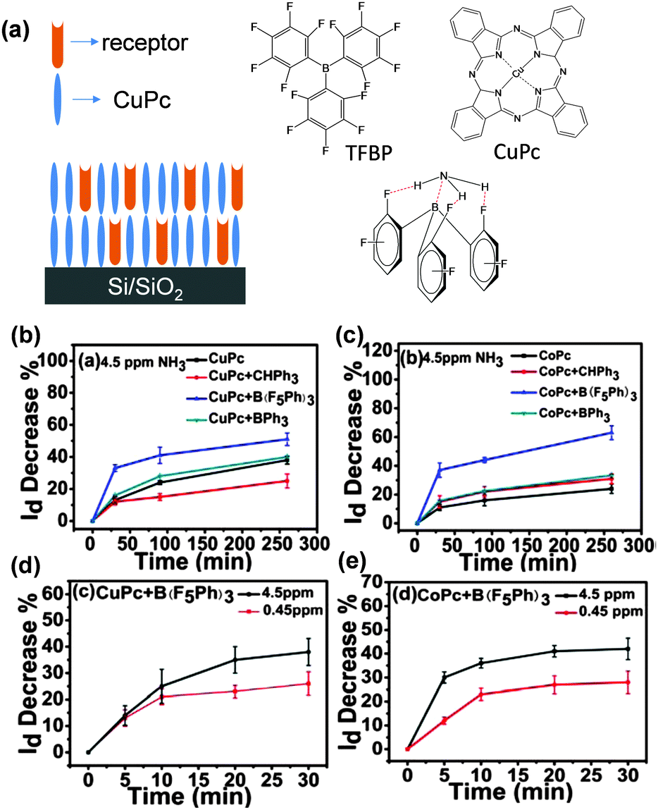 | ||
| Fig. 4 (a) Schematic diagram of mixed films with receptor embedded, molecular structures and interaction between TFBP and NH3; (b–e) drain current decrease of different films with and without receptor molecules. Reproduced with permission from ref. 34. | ||
The other point of applying multiple components is to utilize the hetero-junction between organic–organic interfaces or to introduce a specific texture for gas absorption/diffusion to improve the sensitivity of the device.35–37 H. W. Katz et al. have brought up the concept of using blended layers to enhance the sensing ability by introducing more boundaries and pinholes in the ultra-thin films with the prerequisite of maintaining efficient charge transport along the conductive channel.15 The blended layers present a high and reproducible response to 5 ppm DMMP, which is better than that of single layers. D. Yan et al. demonstrated two-layer films using para-sexiphenyl (p-6P) and N,N′-di-phenyl perylene tetracarboxylic diimide (PTCDI-Ph) in which neither of the ultra-thin single layers is sensitive to NO2, but the as-formed planar heterostructural films present significantly improved sensitivity (Fig. 5a–d).38 By further decoration with the third component vanadyl phthalocyanine (VOPc), they obtained a sensor with sensitivity higher than 500% to 20 ppm NO2 at room temperature accompanied by a fast response and recovery speed (Fig. 5e and f). The reason for the increase in sensitivity was ascribed to the heterojunction effect between the organic–organic interfaces in addition to the improved morphology factor. p-6P and PTCDI-Ph formed a heterojunction that induced additional electrons that accumulated on the PTCDI-Ph layer. The decorated VOPc layer formed another heterojunction with the PTCDI-Ph layer, which induced more electrons on the side of the PTCDI-Ph layer. These accumulated electrons significantly improved the conductivity, and enhanced the charge transfer with NO2, thus leading to improved sensitivity.
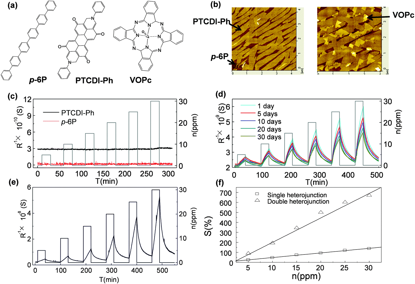 | ||
| Fig. 5 (a) Molecular structure of p-6P, PTCDI-Ph and VOPc; (b) AFM height images of p-6P/PTCDI-Ph and p-6P/PTCDI-Ph/VOPc; (c) the response of a single layer to NO2 exposure; (d) the response of p-6P/PTCDI-Ph in 30 days; (e) the response of p-6P/PTCDI-Ph/VOPc to NO2; (f) the relative response of bilayer and trilayer films to different concentrations of NO2. Reproduced with permission from ref. 38. | ||
4. Organic nanocrystals
Another type of candidate that has drawn attention is the organic nanostructure, such as nanocrystals or single crystals. Similar to inorganic nanostructures, these organic nanocrystals that have a one- or zero-dimensional nanostructure are attractive because of their high specific surface area with good charge transport ability, and thus, they could serve as an active layer in both resistor- and transistor-type sensors.16,31,32 Polymer fiber crystals, as one representative example, exhibit promising potential in chemiresistor-type sensors.39Fig. 6a–d shows the morphology of electrospinning PANi fibers that consist of nanofibers with a uniform size distribution at different contents of doping agents. Those fiber-based resistor gas sensors (Fig. 6e) present an extremely high response to NH3 and NO2 gases. The sensors present a resistance change of up to 3000% to 500 ppm NH3 with reproducible responses (Fig. 6f), while maintaining a fast response and recovery process (the response and recovery time is approximately 45 s and 70 s, respectively). The response to NO2 is even better in that exposure to 20 ppm will decrease the resistance from 106 to 102 Ω (Fig. 6g).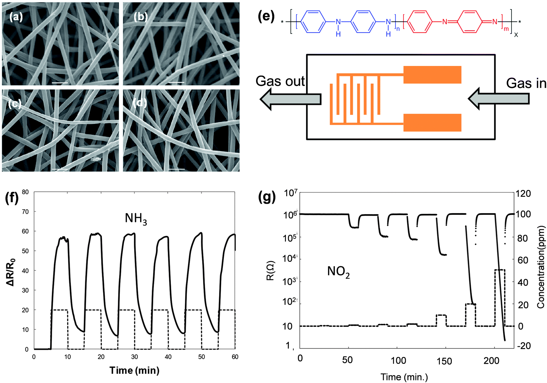 | ||
| Fig. 6 (a–d) SEM image of the PANi fibers; (e) molecular structure and the device configuration of the resistor gas sensor; (f) the response to NH3; (g) the response to NO2. Reproduced with permission from ref. 39. | ||
Nanocrystals of small molecules also perform in an impressive manner. Micro/nanocrystals of perylene diimide derivatives (PTCDIs) that were previously studied in fluorescent gas sensors can also act as electrical gas sensors and exhibit a high sensitivity to reducing gases, such as hydrazine or ammonia.40–42 Y. Huang et al. synthesized a series of PTCDI nanobelts and nanotubes using the solution method and measured the response to hydrazine or NH3 based on either a single or a network of nanocrystal resistors. The substitutions on PTCDIs will lead to significant variations in gas sensing, but a full explanation of the mechanism is still unclear. Y. Liu et al. reported a transistor type gas sensor based on a single CuPc nanowire that first demonstrated the high sensitivity of organic materials to SO2 (Fig. 7a and b).43 The response to periodic pulses of SO2 and corresponding sensitivity are demonstrated in Fig. 7c and d. The high sensitivity mainly originates from the gas dielectric configuration that the CuPc nanowire potentially places on the gate substrate. Such a gas dielectric configuration enhances gas absorption at the dielectric/active layer interface and accordingly increases the sensitivity because the effective charge transport channel of organic transistors is located on the layer close to the dielectric surface (Fig. 7c and d). A comparison with non-floated nanowire devices confirmed that the effective absorption critically relies on the dielectric/nanowire interface rather than on the side or top surface of the nanowire as the authors noted. This might be a new outlook on the mechanism, which still needs to be proved.
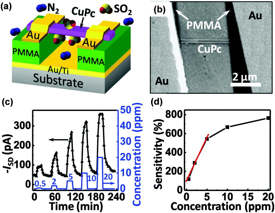 | ||
| Fig. 7 (a) Configuration of the gas dielectric transistor with a single wire of CuPc as the active layer; (b) the SEM image of the device; (c) the drain current evolution on exposure to different concentrations of SO2; (d) the sensitivity of the sensor to different concentrations of SO2. Reproduced with permission from ref. 43. | ||
5. Organic molecule decorated inorganic nanostructure
A pure organic molecular active layer has some apparent shortcomings such as low conductivity and stability compared to its inorganic counterparts. Nanostructured inorganic materials represent one of the best and most extensively investigated candidates in the field of gas sensors, because of their high surface-to-volume ratio, stable conductivity and mature fabrication technology but they are limited by their poor selectivity.16,18,19,44–47 Assembling organic molecules onto a more stable inorganic nanostructure is a promising strategy for solving both the conductivity and stability issues of organic materials, and the selectivity of inorganic materials. Two approaches for assembling organic materials onto inorganic nanostructures are usually applied. One is simply depositing organic materials onto inorganic nanostructures to form organic–inorganic mixtures or networks, wherein only physical absorption occurs between the two components. The other is assembling the organic molecules onto the nanostructure through chemical bonding utilizing some strong bonding interaction, such as S–Au, O–Si and so on. In these organic–inorganic hybrid systems, the organic components act as receptors or recognition sites for specific gases, while the inorganic components undertake the charge transport role. The goal is to achieve a synergistic effect between the inorganic and organic materials.48–52The common approach to the physisorption type is demonstrated in Fig. 8. Using a carbon nanotube as an example, the Haick group fabricated organic–inorganic mixtures by deposition of a series of polycyclic aromatic hydrocarbon (PAH) compounds onto carbon nanotube networks.48 With the recognition molecules on the nanotube, besides the significantly improved sensitivity, they can discriminate among several polar and nonpolar volatile organic compounds by comparing their sensitivity to different concentrations under the conditions of variable humidity. Fig. 9 shows image plots of the sensitivity of a hybrid film and pristine SCWNT on exposure to different concentrations of VOCs and water. Obviously, the addition of the PAH layer improved the response to some VOCs compared with the pristine SCWNT. In addition, some PAH derivatives with specific groups show a high response to OH-terminated polar VOCs. Such different responses effectively increased the discrimination among different analytes, thus increasing the selectivity.
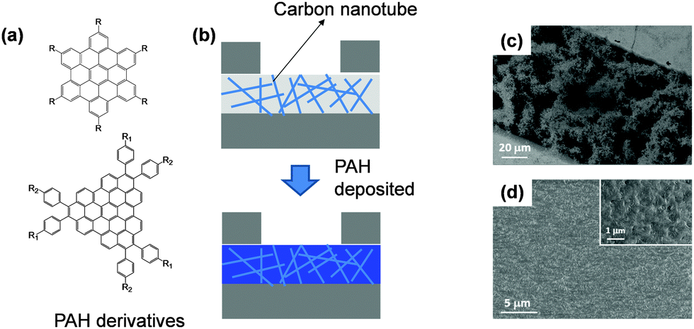 | ||
| Fig. 8 (a) Molecular structures of PAH derivatives; (b) device configuration of the organic–inorganic network; (c) SEM image of the active layer with only carbon nanotubes; (d) SEM image of the organic–inorganic active layer after deposition of organic materials. Reproduced with permission from ref. 48. | ||
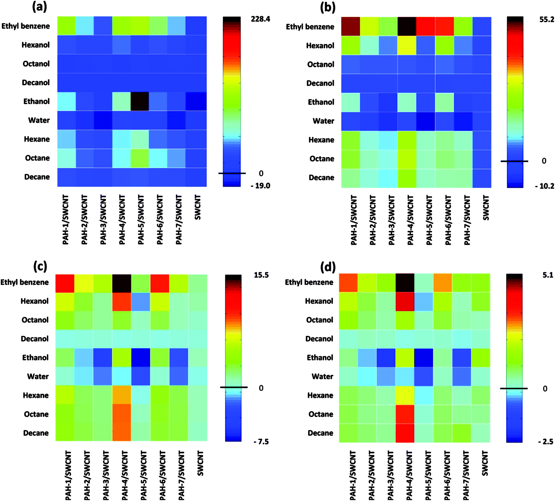 | ||
| Fig. 9 Image plots of sensitivity to different VOCs with different concentrations and water. (a) 1; (b) 0.5; (c) 0.2; (d) 0.09. Reproduced with permission from ref. 48. | ||
The sensing mechanism of such organic–inorganic mixtures is still unclear. Besides the charge transfer between recognition molecules and the analyte, other effects were reported to account for the change in the sensing signal.53–56 The swelling effect is one of the important factors, especially in the carbon nanotube–polymer composite systems. The polymer matrix will expand when exposed to the analyte, which results in a change of the inter-tube distance as well as conductivity. Such a swelling effect was also observed for small molecule thin films, as suggested from the mass or thickness signal change by quartz crystal microbalance and spectroscopic ellipsometry. The Haick group found that polycyclic aromatic hydrocarbon derivatives presented a more obvious mass or thickness change when exposed to certain nonpolar analytes than polar analytes. Such a swelling effect should be concerned especially when humidity is at a high level. Besides the thickness or mass change, the swelling of films when exposed to nonpolar analytes was found to change the conductivity or work function of the carbon nanotube, which should be attributed to the carrier scattering effect. Understanding such an effect will help design electrical gas sensors for nonpolar analytes, which lack charge transfer in most cases.
H. Haick et al. also developed gas sensors based on silicon nanowires on which a series of organic functional molecules were chemically absorbed.50,57–60 The silane molecules with different end groups were attached to the single silicon nanowire through self-assembling technology (Fig. 10a) and served together as transistor sensors to react with different volatile organic compounds. The resulting sensors demonstrate an end-group dependent transistor performance when exposed to different organic analytes to track the variation in their transistor parameters. Fig. 10b–e summarizes the threshold voltage variation for different analytes with different silane molecules. The parameter variation is mainly related to the interaction between the functional group and the analytes, which is ascribed to three scenarios: the dipole–dipole interaction between molecular layers with polar VOCs, the induced dipole–dipole interaction between molecular layers with nonpolar VOCs and molecular layer tilt as a result of VOC diffusion. Fig. 10f illustrates the relationship between the threshold voltage variation and the gas–molecule interaction. Upon exposure to polar or nonpolar VOCs, the electron-donating or withdrawing end groups on the functional molecule will produce a variation of dipole moment because of these dipole interactions, thus causing a shift in ΔVth. The results indicated that for polar VOCs, because of the strong dipole–dipole interaction, a larger variation of ΔVth is always observed, while the direction of variation is different for electron donating and withdrawing groups. Such a selective and varied response enhanced the sensitivity and selectivity compared to SiNWs without molecular antennas. Importantly, with a variation in only one parameter in such a system, it is still not easy to clarify different analytes. Therefore, the Haick group developed a method for precise discrimination by analyzing different parameter variations, similar to constructing a fingerprint for each gas to provide accurate discrimination.58,60
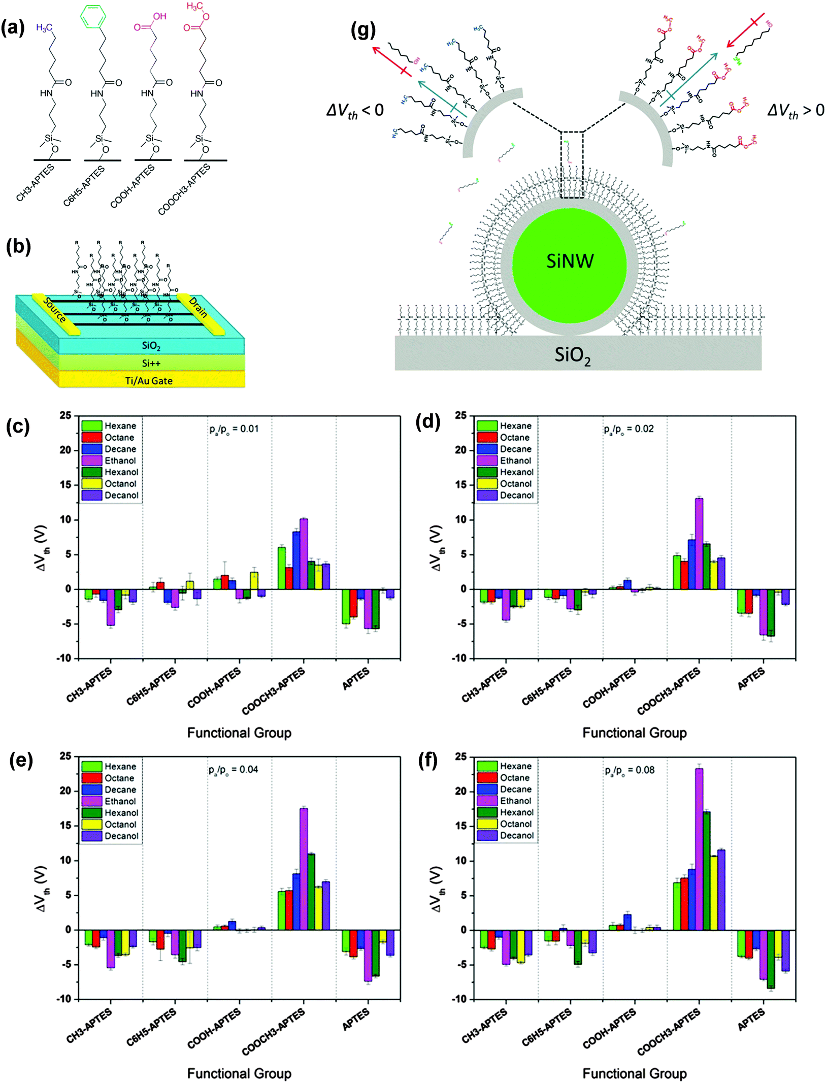 | ||
| Fig. 10 (a) Molecular structure of the self-assembled molecules; (b) configuration of the transistor sensors with SAM-Si NWs as the active layer; (c–f) the threshold voltage variation of different SAMs to different VOCs with different concentrations; (g) the interaction between SAM and the analytes and their influence on the threshold voltage variation. Reproduced with permission from ref. 50. | ||
The other method for accurate identification is to develop individual sensors that specifically respond to a specific analyte. H. Shen et al. reported a SAM–SnO2 system that shows an obvious specific response to the NO2 analyte.52 Similarly, they utilized silane molecules, but with primary, secondary, tertiary and mixed amine terminals as receptors that were attached to the SnO2 NW via chemical bonding (Fig. 11a and b). Fig. 11c illustrates the interaction between an amine–silane molecule and NO2 at different stages. The results indicate that the amine groups significantly enhanced the response to NO2 (Fig. 11d–g). It presents a high sensitivity of 2100% to 0.4 ppm NO2, which represents one of the best levels of sensitivity achieved. It is even more important to know that only a small or insignificant response can be detected by other gases such as SO2, NO, and NH3. This indicates a specific selectivity to the NO2 analyte.
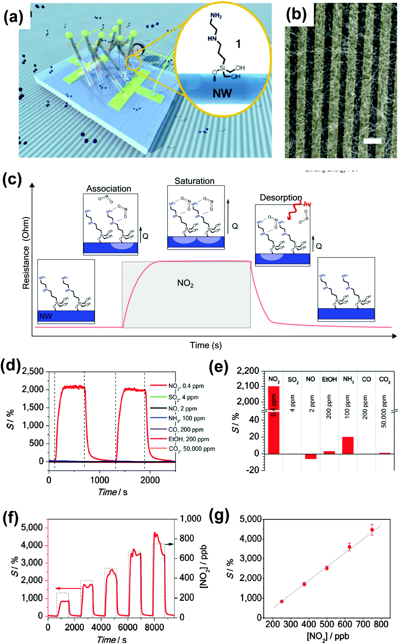 | ||
| Fig. 11 (a) Schematic diagram of the resistor gas sensor with SAM–SnO2 as the active layer, inset: diagram of silane molecule attached on SnO2 NW; (b) SEM images of the SAM–SnO2 active layer with electrodes; (c) schematic diagram of the interaction between the SAM molecule and NO2 and the corresponding response to the sensing signal; the relative sensitivity of the gas sensor to (d and e) different gases; (f and g) to NO2 with varied concentrations. Reproduced with permission from ref. 52. | ||
6. Discussion and perspectives
The studies presented above demonstrate the advantage of versatile textures of the active layer in developing a high performance gas sensor, but a precise mechanism is still lacking for organic materials.26,33,61–63 Nevertheless, we can summarize some general rules based on the physical process of electrical gas sensors. The fundamental issue is a detectable conductivity; in other words, an efficient charge transport ability is needed to guarantee successful operation. Beyond this level, the issues critically rely on three processes, i.e., gas absorption, diffusion and desorption. The reversible gas absorption and desorption generate a variation in carrier density or traps in the films which is reflected in the electrical parameters, such as conductivity, mobility or threshold voltage. The intrinsic properties of the molecules used as the active layer determine the charge transfer or other interactions with the analytes, which mainly influence the gas absorption/desorption kinetics when the gas is in contact with the molecules. Such a charge transfer or interaction process is reflected in the selectivity and response/recovery of sensors. The modulation of the active layer's texture can effectively tune the charge transport ability by changing the ordering, thickness and packing, as well by monitoring the gas kinetics (absorption, diffusion and desorption) and controlling the surface-to-volume ratio, thickness, grain size or alignment.For traditional bulk or thick films (Fig. 12a), the gas analytes will interact through the surface of the materials/films and gradually diffuse into the inner layer, causing the gradual response process that is commonly observed. When the analyte flow is switched off, gases in the inner layer require a long time to diffuse out and thus a long time to desorb, leading to slow recovery. With a reduced one-dimensional size such as thickness to one or few monolayers, the organic active layer can be regarded as a flat surface covered by the active molecules (Fig. 12b). Thus the imposed analyte only needs to go through a surface absorption process or a short diffusion path before the charge transfer occurs, leading to a fast response. For the desorption process, the gas likewise only needs a short path to leave the active layer, hence shortening the recovery process. If the other dimensions are further modulated to form stripes or nanocrystals, the one-dimensional continuous texture provides a more exposed surface for absorption and a shorter path for diffusion, thus improving the sensor performance (Fig. 12c).
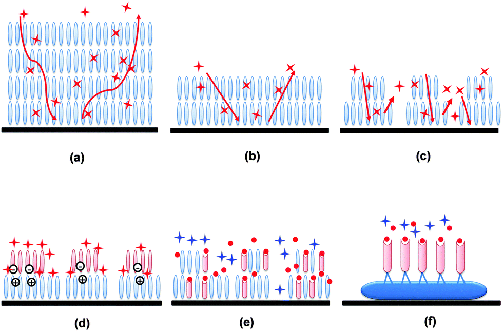 | ||
| Fig. 12 Schematic diagram of the gas absorption, diffusion and desorption processes demonstrating the influence of different textures. (a) Thick films; (b) ultra-thin films; (c) one-dimensional structured films; (d) heterostructure films; (e) mixed film with receptors; (f) organic–inorganic hybrid structure. | ||
The above explanation only considers the gas kinetics aspect. When the interactions between the gas and the active layer molecules are taken into account, the modulation of molecular engineering beyond the texture will greatly affect the sensing performance. An optimized layer thickness is also expected. One case is to utilize the heterojunction effect between different organic components to induce a partial charged interface (Fig. 12d), which would increase the gas–surface interaction due to the more dipolar character of the surface. The other case is that the receptor sites are imposed in the film or nanostructure system, as in those introduced by the Katz or Haick group. The imposed receptor molecules act as antennas to efficiently recognize and absorb specific analytes because of the receptor–analyte interaction. This will result in a selective response to specific analytes with high sensitivity and fast response/recovery, as displayed in Fig. 12e and f. If using more stable inorganic nanostructures as conductive materials, a reproducible high-sensitivity gas sensor with high selectivity is expected. In terms of extensive research in this field, the texture modulation combined with molecular engineering will be a promising approach for achieving high-performance gas sensors with reliable properties.
In general, although great progress has been achieved targeting room-temperature high-performance gas sensors through different strategies from the materials or morphology perspective, the challenges for these sensors becoming real products are obvious. Some key issues such as the compatibility between organic and inorganic materials, the accurate discrimination of analytes, the reproducibility and stability of those structured films or nanostructures and their gas sensing performance, as well as the mechanism of organic materials or hybrid materials are still the subjects of intensive investigations. We believe that this field still holds great potential if these problems are addressed with further studies on both fundamental science and technological development.
Acknowledgements
We acknowledge the financial support from the National Natural Science Foundation of China (91227201, 11304213, 51503138, 21527805), China Postdoctoral Science Foundation (2014M550304, 2015T80579) and Suzhou Industrial Park (SUN-WIN project 2013). And we thank the support from the Collaborative Innovation Center of Suzhou Nano Science & Technology and the Priority Academic Program Development of Jiangsu Higher Education Institutions.Notes and references
- X. Liu, S. Cheng, H. Liu, S. Hu, D. Zhang and H. Ning, Sensors, 2012, 12, 9635–9665 CrossRef PubMed.
- R. M. Crooks and A. J. Ricco, Acc. Chem. Res., 1998, 31, 219–227 CrossRef CAS.
- A. J. Ricco, R. M. Crooks and G. C. Osbourn, Acc. Chem. Res., 1998, 31, 289–296 CrossRef CAS.
- M. Tiemann, Chem. – Eur. J., 2007, 13, 8376–8388 CrossRef CAS PubMed.
- L. Torsi and A. Dodabalapur, Anal. Chem., 2005, 77, 380A–387A CrossRef CAS PubMed.
- M. E. Roberts, A. N. Sokolov and Z. Bao, J. Mater. Chem., 2009, 19, 3351–3363 RSC.
- C. Zhang, P. Chen and W. Hu, Chem. Soc. Rev., 2015, 44, 2087–2107 RSC.
- L. Torsi, M. Magliulo, K. Manoli and G. Palazzo, Chem. Soc. Rev., 2013, 42, 8612–8628 RSC.
- B. Bott and T. A. Jones, Sens. Actuators, 1984, 5, 43–53 CrossRef CAS.
- T. A. Jones, B. Bott and S. C. Thorpe, Sens. Actuators, 1989, 17, 467–474 CrossRef CAS.
- T. Someya, H. E. Katz, A. Gelperin, A. J. Lovinger and A. Dodabalapur, Appl. Phys. Lett., 2002, 81, 3079 CrossRef CAS.
- J. Locklin and Z. Bao, Anal. Bioanal. Chem., 2006, 384, 336–342 CrossRef CAS PubMed.
- T. Someya, A. Dodabalapur, J. Huang, K. C. See and H. E. Katz, Adv. Mater., 2010, 22, 3799–3811 CrossRef CAS PubMed.
- R. D. Yang, T. Gredig, C. N. Colesniuc, J. Park, I. K. Schuller, W. C. Trogler and A. C. Kummel, Appl. Phys. Lett., 2007, 90, 263506 CrossRef.
- J. Huang, J. Sun and H. E. Katz, Adv. Mater., 2008, 20, 2567–2572 CrossRef CAS.
- B. Li and D. N. Lambeth, Nano Lett., 2008, 8, 3563–3567 CrossRef CAS PubMed.
- M. E. Roberts, S. C. B. Mannsfeld, M. L. Tang and Z. Bao, Chem. Mater., 2008, 20, 7332–7338 CrossRef CAS.
- Y. F. Sun, S. B. Liu, F. L. Meng, J. Y. Liu, Z. Jin, L. T. Kong and J. H. Liu, Sensors, 2012, 12, 2610–2631 CrossRef CAS PubMed.
- X. Zhao, B. Cai, Q. Tang, Y. Tong and Y. Liu, Sensors, 2014, 14, 13999–14020 CrossRef PubMed.
- B. Kang, M. Jang, Y. Chung, H. Kim, S. K. Kwak, J. H. Oh and K. Cho, Nat. Commun., 2014, 5, 4752 CrossRef CAS PubMed.
- H. Chen, S. Dong, M. Bai, N. Cheng, H. Wang, M. Li, H. Du, S. Hu, Y. Yang, T. Yang, F. Zhang, L. Gu, S. Meng, S. Hou and X. Guo, Adv. Mater., 2015, 27, 2113–2120 CrossRef CAS PubMed.
- R. Vishinkin and H. Haick, Small, 2015, 11, 6142–6164 CrossRef CAS PubMed.
- N. S. Ramgir, Y. Yang and M. Zacharias, Small, 2010, 6, 1705–1722 CrossRef CAS PubMed.
- G. Konvalina and H. Haick, Acc. Chem. Res., 2014, 47, 66–76 CrossRef CAS PubMed.
- M. Meyyappan, Small, 2016, 12, 2118–2129 CrossRef CAS PubMed.
- F. I. Bohrer, A. Sharoni, C. Colesniuc, J. Park, I. K. Schuller, A. C. Kummel and W. C. Trogler, J. Am. Chem. Soc., 2007, 129, 5640–5646 CrossRef CAS PubMed.
- J. Huang, J. Miragliotta, A. Becknell and H. E. Katz, J. Am. Chem. Soc., 2007, 129, 9366–9376 CrossRef CAS PubMed.
- F. Zhang, C. A. Di, N. Berdunov, Y. Hu, Y. Hu, X. Gao, Q. Meng, H. Sirringhaus and D. Zhu, Adv. Mater., 2013, 25, 1401–1407 CrossRef CAS PubMed.
- X. Wang, S. Ji, H. Wang and D. Yan, Sens. Actuators, B, 2011, 160, 115–120 CrossRef CAS.
- L. Li, P. Gao, M. Baumgarten, K. Mullen, N. Lu, H. Fuchs and L. Chi, Adv. Mater., 2013, 25, 3419–3425 CrossRef CAS PubMed.
- B. Dong, D. Y. Zhong, L. F. Chi and H. Fuchs, Adv. Mater., 2005, 17, 2736–2741 CrossRef CAS.
- B. Dong, N. Lu, M. Zelsmann, N. Kehagias, H. Fuchs, C. M. Sotomayor Torres and L. F. Chi, Adv. Funct. Mater., 2006, 16, 1937–1942 CrossRef CAS.
- S. Ji, X. Wang, C. Liu, H. Wang, T. Wang and D. Yan, Org. Electron., 2013, 14, 821–826 CrossRef CAS.
- W. Huang, K. Besar, R. LeCover, A. M. Rule, P. N. Breysse and H. E. Katz, J. Am. Chem. Soc., 2012, 134, 14650–14653 CrossRef CAS PubMed.
- R. D. Yang, J. Park, C. N. Colesniuc, I. K. Schuller, J. E. Royer, W. C. Trogler and A. C. Kummel, J. Chem. Phys., 2009, 130, 164703 CrossRef PubMed.
- X. Wang, S. Ji, H. Wang and D. Yan, Org. Electron., 2011, 12, 2230–2235 CrossRef CAS.
- M. Z. Dai, Y. L. Lin, H. C. Lin, H. W. Zan, K. T. Chang, H. F. Meng, J. W. Liao, M. J. Tsai and H. Cheng, Anal. Chem., 2013, 85, 3110–3117 CrossRef CAS PubMed.
- S. Ji, H. Wang, T. Wang and D. Yan, Adv. Mater., 2013, 25, 1755–1760 CrossRef CAS PubMed.
- Y. Zhang, J. J. Kim, D. Chen, H. L. Tuller and G. C. Rutledge, Adv. Funct. Mater., 2014, 24, 4005–4014 CrossRef CAS.
- Y. Huang, J. Wang, L. Fu, W. Kuang and J. Shi, Sens. Actuators, B, 2013, 188, 411–416 CrossRef CAS.
- Y. Huang, L. Fu, W. Zou, F. Zhang and Z. Wei, J. Phys. Chem. C, 2011, 115, 10399–10404 CAS.
- Y. Huang, W. Zhang, J. Wang and Z. Wei, ACS Appl. Mater. Interfaces, 2014, 6, 9307–9313 CAS.
- T. Shaymurat, Q. Tang, Y. Tong, L. Dong and Y. Liu, Adv. Mater., 2013, 25, 2269–2273 CrossRef CAS PubMed , 2376.
- J. Li, Y. J. Lu, Q. Ye, M. Cinke, J. Han and M. Meyyappan, Nano Lett., 2003, 3, 929–933 CrossRef CAS.
- J. Zhang, S. Wang, M. Xu, Y. Wang, B. Zhu, S. Zhang, W. Huang and S. Wu, Cryst. Growth Des., 2009, 9, 3532–3537 CAS.
- P. Feng, F. Shao, Y. Shi and Q. Wan, Sensors, 2014, 14, 17406–17429 CrossRef PubMed.
- L. Valentini, I. Armentano, J. M. Kenny, C. Cantalini, L. Lozzi and S. Santucci, Appl. Phys. Lett., 2003, 82, 961 CrossRef CAS.
- Y. Zilberman, R. Ionescu, X. Feng, K. Müllen and H. Haick, ACS Nano, 2011, 5, 6743–6753 CrossRef CAS PubMed.
- M. D. Shirsat, T. Sarkar, J. Kakoullis, Jr., N. V. Myung, B. Konnanath, A. Spanias and A. Mulchandani, J. Phys. Chem. C, 2012, 116, 3845–3850 CAS.
- B. Wang and H. Haick, ACS Appl. Mater. Interfaces, 2013, 5, 2289–2299 CAS.
- M. W. G. Hoffmann, J. D. Prades, L. Mayrhofer, F. Hernandez-Ramirez, T. T. Järvi, M. Moseler, A. Waag and H. Shen, Adv. Funct. Mater., 2014, 24, 595–602 CrossRef CAS.
- M. Kimura, R. Sakai, S. Sato, T. Fukawa, T. Ikehara, R. Maeda and T. Mihara, Adv. Funct. Mater., 2012, 22, 469–476 CrossRef CAS.
- C. Wei, L. Dai, A. Roy and T. B. Tolle, J. Am. Chem. Soc., 2006, 128, 1412–1413 CrossRef CAS PubMed.
- H. J. Salavagione, A. M. Díez-Pascual, E. Lázaro, S. Vera and M. A. Gómez-Fatou, J. Mater. Chem. A, 2014, 2, 14289 CAS.
- N. Bachar, L. Mintz, Y. Zilberman, R. Ionescu, X. Feng, K. Mullen and H. Haick, ACS Appl. Mater. Interfaces, 2012, 4, 4960–4965 CAS.
- G. Peng, U. Tisch and H. Haick, Nano Lett., 2009, 9, 1362–1368 CrossRef CAS PubMed.
- Y. Paska, T. Stelzner, O. Assad, U. Tisch, S. Christiansen and H. Haick, ACS Nano, 2012, 6, 335–345 CrossRef CAS PubMed.
- R. Ermanok, O. Assad, K. Zigelboim, B. Wang and H. Haick, ACS Appl. Mater. Interfaces, 2013, 5, 11172–11183 CAS.
- B. Wang and H. Haick, ACS Appl. Mater. Interfaces, 2013, 5, 5748–5756 CAS.
- A. Bayn, X. Feng, K. Mullen and H. Haick, ACS Appl. Mater. Interfaces, 2013, 5, 3431–3440 CAS.
- J. H. Park, J. E. Royer, E. Chagarov, T. Kaufman-Osborn, M. Edmonds, T. Kent, S. Lee, W. C. Trogler and A. C. Kummel, J. Am. Chem. Soc., 2013, 135, 14600–14609 CrossRef CAS PubMed.
- A.-M. Andringa, C. Piliego, I. Katsouras, P. W. M. Blom and D. M. d. Leeuw, Chem. Mater., 2014, 26, 773–785 CrossRef CAS.
- W. Huang, J. Sinha, M.-L. Yeh, J. F. M. Hardigree, R. LeCover, K. Besar, A. M. Rule, P. N. Breysse and H. E. Katz, Adv. Funct. Mater., 2013, 23, 4094–4104 CrossRef CAS.
| This journal is © The Royal Society of Chemistry 2016 |