
Photodynamic assembly of nanoparticles towards designable patterning
Huan
Wang
a,
Yong-Lai
Zhang
*a,
Hong
Xia
a,
Qi-Dai
Chen
a,
Kwang-Sup
Lee
b and
Hong-Bo
Sun
*ac
aState Key Laboratory on Integrated Optoelectronics, College of Electronic Science and Engineering, Jilin University, 2699 Qianjin Street, Changchun, 130012, P. R. China. E-mail: yonglaizhang@jlu.edu.cn; hbsun@jlu.edu.cn; Fax: +86-431-85168281; Tel: +86-431-85168281
bDepartment of Advanced Materials, Hannam University, Daejeon, South Korea
cCollege of Physics, Jilin University, 119 Jiefang Road, Changchun, 130023, P. R. China
First published on 9th November 2015
Abstract
Recent advancements in nanotechnology have continued to stimulate the development of functional devices based on nanomaterials. However, the controllable assembly of these tiny nanomaterials into functional structures is still a big challenge for further applications; nowhere is this more obvious than in the field of nanodevices. Currently, despite the fact that self-assembly technologies have revealed great potential to reach this end, serious problems with respect to morphology control, designable assembly and even flexible patterning set huge obstacles to the fabrication of functional devices. Nowadays, in addition to self-assembly technologies that make use of interaction forces between different objects, photodynamic assembly (PDA) technology has emerged as a promising route to architect functional materials with the help of optical driving forces towards device fabrication. In this review, we summarize the recent developments in PDA technology for the designable patterning of nanoparticles (NPs). The basic fundamentals of PDA that resort to optical trapping (OT) and typical examples regarding far-field/near-field OT for the PDA of various NPs have been reviewed. In particular, femtosecond laser induced photodynamic assembly (FsL-PDA), which enables the designable patterning of NPs through a direct writing manner, has been introduced. Finally, the current challenges and future prospects of this dynamic field are discussed based on our own opinions.
 Huan Wang | Huan Wang received his BS from the College of Electronic Science and Engineering (2011), Jilin University. In 2012, he participated in the National Key Basic Research Program about Lab-on-a-Chip systems in the Institute of Semiconductors, Chinese Academy of Science. He is currently a PhD student in the State Key Laboratory of Integrated Optoelectronics, Jilin University. His research interests include Lab-on-a-Chip systems, MEMS, laser micronanofabrication, and especially femtosecond laser induced photodynamic assembly and photopolymerization. |
 Yong-Lai Zhang | Yong-Lai Zhang received his BS (2004) and PhD (2009) from Jilin University, China. After receiving his PhD, he joined the faculty in the State Key Laboratory on Integrated Optoelectronics, College of Electronic Science and Engineering, Jilin University. In 2011, he worked as a research professor in Yonsei University, Korea. After that, he was awarded a “Hong Kong Scholar” postdoctoral fellowship and worked at the Center of Super Diamond and Advanced Films (COSDAF), City University of Hong Kong. His research interests include laser micronanofabrication of functional micronanostructures, smart actuators and Bio-MEMS. |
 Kwang-Sup Lee | Kwang-Sup Lee is a professor at the Department of Advanced Materials at Hannam University, Korea. He also holds the position of Research Professor at the Institute for Lasers, Photonics and Biophotonics in the University at Buffalo, SUNY. He received his BS degree in chemistry from Hannam University in 1976, MS degree in polymer chemistry from Korea University in 1980, and a doctorate in polymer science from Freiburg University, Germany in 1984. His research interests lie in the field of photofunctional polymers, organic–inorganic hybrid materials and their application in devices. Prof. Lee is a Fellow of SPIE and the EM Academy. |
 Hong-Bo Sun | Hong-Bo Sun received his PhD from Jilin University, China, in 1996. He worked as a postdoctoral researcher in the University of Tokushima, Japan, from 1996 to 2000, and then as an assistant professor in the Department of Applied Physics, Osaka University. He became a project leader in 2001. He was awarded by the Optical Science and Technology Society in 2002, and won Outstanding Young Scientist Award issued by the minister of MEXT (Japan) in 2006. In 2005, he became a professor (Changjiang Scholar) at Jilin University. His research is focused on laser micro-nanofabrication, and its applications in microoptics, micromachines, microfluids, and microsensors. |
1. Introduction
Recent decades have seen great advancement be achieved in both nanotechnology and materials science.1–5 Consequently, novel functional devices based on nanomaterials have evolved rapidly with huge impetus. Nowadays, with the progress in synthetic methodology, nanomaterials with tunable size, morphology and composition can be readily prepared through a variety of methods like chemical synthesis,6–9 laser ablation,10,11 polymerization12,13 and chemical etching.14,15 Among those nanoscale materials, nanoparticles (NPs) are well investigated, since these tiny particles with average sizes in the range from several to tens of nanometers exhibit superior properties as compared with their bulk materials.16 Owing to their outstanding properties, NPs are employed for a broad spectrum of applications in optics,17,18 catalysis,19–21 sensors,22 electronics,23,24 medical diagnosis and treatment.25–27 However, the use of NPs also encounters many troubles. For instance, it is quite difficult to manipulate such tiny particles in a controlled fashion, which sets huge obstacles to the fabrication of functional nanodevices, since it is generally necessary to control the location of NPs accurately for device integration.28,29 Moreover, the application of NPs also suffers from problems with respect to separation, collection, and assembly.To get better control of the tiny NPs, novel assembly technologies have been developed to construct functional materials, among which the self-assembly of NPs is established as a useful approach. Typically, NPs with various surface-capping ligands could be used as nano-building blocks;30–32 and the interactions including covalent bonds,33,34 electrostatic attraction,35–38 and van der Waals forces39,40 have been adopted as the driving force to guide the assembly. Notably, the elaborate modification of the surface-capping ligands or the moieties of the surfactant templates could control the assembly process and even lead to the formation of NP patterns.41 In this case, complex and precise chemical modification is needed to arrange force fields. Besides, DNA, virus and protein templates have been successfully used for NP assembly.42,43 The sizes and mechanical properties of DNA templates could be easily controlled; thus the DNA-origami strategy enables the construction of almost arbitrary DNA configurations. Due to the strong interactions between metal particles and DNA, these templates are widely used for colloidal particle assembly.44,45 External force fields, such as electrostatic forces and magnetic forces, are also adopted to assist the assembly of NPs;46–49 however, the resulting structures show very low resolution, since it is quite difficult to confine an external field at the micro/nanoscale. We have previously demonstrated the possibility of ordering quantum dots via photoinduced polymerization of surface ligands.50,51 Additionally, self-assembly can be achieved at the interfaces by carefully modulating the interfacial tensions between two phases, which has also been reported for NP assembly.52 To date, despite the fact that self-assembly technologies have revealed great potential to realize NP assembly, serious problems with respect to morphology control, designable patterning and even non-planar assembly set huge obstacles to the fabrication of functional devices. Currently, the controllable assembly of NPs into functional structures is still a big challenge for further applications, nowhere is this more obvious than in the development of nanodevices.
Techniques like photolithography, nanoimprinting,53,54 and ink-jet printing55,56 popular in the semiconductor industry have been applied in the past to fabricate pre-patterned substrates for templating NP self-assembly and patterns. However, the procedure is usually very complex. Moreover, the process is not compatible with device fabrication/integration, since only very flat and smooth surfaces are compatible with such techniques. Alternatively, as a non-contact and non-destructive method, optical forces are capable of manipulating NPs precisely, which provides the feasibility to make nanodevices using NPs.57–61 With the help of optical trapping (OT) forces, the tiny NPs could be picked up and placed at any desired position; in this way, NPs could be patterned flexibly.62–66 Theoretically, NPs are polarized by optical fields,67 and considered as charged particles. When the charged particles move in magnetic fields, the Lorentz forces that could trap and move NPs in optical fields are generated accordingly. Modern optics allows the production of beams with desired wavelengths, phases, power, and almost all of the parameters of light, which enables precise control over Lorentz forces; in this way, NPs could be assembled flexibly.68 In this review, we first discuss the fundamentals of the photodynamic assembly (PDA) of NPs. Generally, optical fields induce relatively stationary potential fields; NPs could be trapped exactly in the potential wells where the potential energy of the NPs is the lowest. Then, the latest reports on near/far-field optics trapping for the PDA of NPs are introduced, respectively. Besides, the femtosecond laser induced photodynamic assembly (FsL-PDA) of NPs has been briefly reviewed, since FsL-PDA shows great potential for the flexible patterning of NP patterns with high resolution. Finally, a brief perspective and conclusion of the PDA of NPs have been made based on our own opinions.
2. Fundamentals of PDA
Generally, when colloidal particles are irradiated by light, two kinds of forces, scattering forces and gradient forces, are exerted on them, which leads to optical pushing, trapping, or pulling under different conditions. If light is scattered among objects, optical bonding (OB) might arise.69,70 It must be pointed out that, in most cases, OT has been utilized to manipulate objects. In 1969, the OT effect was reported for the first time;71 since then, OT has been widely investigated for the remote, noninvasive, accurate control of micro/nanoscale materials, like NPs, carbon nanotubes, quantum dots (QDs), cells, DNA, and enzymes.62,72 However, despite OT having been investigated for almost half a century, the basic principle remains controversial. Nevertheless, a consensus has been reached on two scenarios regarding the size (scale) of the target objects: the geometric optical size (r ≫ λ, r is the radius of the particle, λ is the wavelength of light) and the Rayleigh size (r ≪ λ). When a beam from a high numerical aperture objective irradiates a sphere at a geometric optical scale, the reflected light from the surface and the refracted light through the sphere might diverge from the incident direction, causing the total momentum of the beam to swerve. Consequently, the sphere would be subjected to a force according to the law of conservation of momentum,72 as shown in Fig. 1a. This force could be decomposed into two forces: one is the scattering force, in the direction of the beam; and the other is the gradient force, always pointing to the laser focus. If the sphere is located near the laser focus, the gradient force would dominate the optical forces, so a stable trapping occurs.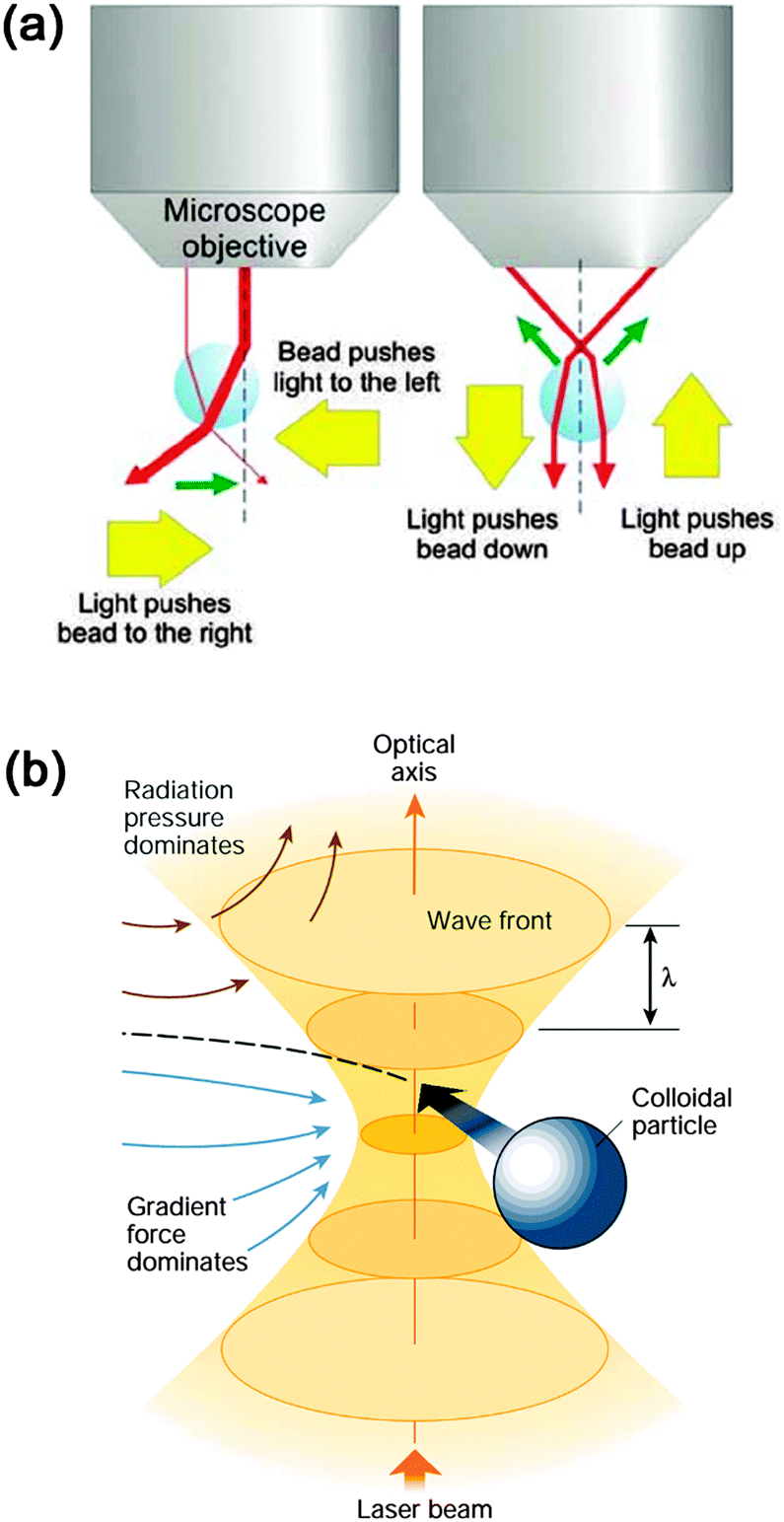 | ||
| Fig. 1 Schematic illustration of the basic principles of OT: NPs at (a) a geometric optical size and (b) a Rayleigh size. (Reproduced from ref. 72 and 73 with the permission of Elsevier and the Nature Publishing Group.) | ||
At the Rayleigh scale, the electromagnetic theory is more convincing.73 It is well known that light is a kind of electromagnetic wave. It is undoubted that NPs would be polarized in the optical fields and they turn out to be dipoles. In a non-uniform optical field, dipoles tend to move to a potential well where they possess the lowest potential energy. Under the conditions of a single beam, the NPs are trapped at the focus of the laser. In other cases, the NPs are trapped at the point where the optical fields are the strongest. The forces exerted on the NPs also could be decomposed into gradient forces and scattering forces. Similarly, the stable trapping of NPs is also dominated by the gradient force. Svoboda et al. calculated the forces and found that both the forces were related to the size and dielectric constant of the NPs.67 With a decrease in the NP size, the gradient force and scattering force diminish at the same time, but the scattering force diminishes more significantly than the gradient force. Therefore, the gradient force dominates the movement of the NPs, leading to stable OT, as shown in Fig. 1b.
On the other hand, the dielectric constant of NPs also affects OT. Metal NPs with higher dielectric constants could be polarized to a greater extent compared to dielectric NPs in non-uniform optical fields. In this regard, it is quite obvious that metal NPs would be manipulated easily. From this point of view, metal NPs with small sizes seem to be suitable for OT towards PDA. For dielectric NPs, a much higher power of beam is generally necessary in order to induce a greater gradient of the electromagnetic field required to induce stable OT. To increase the gradient of electromagnetic fields, optical resonance has been proven to be an effective method. Researchers have created various near-field optics resonance devices or metallic nanostructures for local surface plasma resonance (LSPR) to enhance electromagnetic fields.74 Consequently, the gradient of the electromagnetic field has been significantly increased, leading to strong OT.
The OB phenomenon has attracted more and more attention in recent times.75–78 Scattering light among NPs causes scattering forces that could lead to their bonding, resulting in lattice formation; such lattices are called “optical matter”. Some theoretical assumptions for two particle OB have been presented, but multi-particle bonding has not been clearly described yet. Bain et al. observed OB particle arrays in counter propagating beams and found that the bonding was related to laser polarization and particle sizes;79–81 while Florin et al. calculated the forces that bonded Au NPs.82 To date, despite the fact that many phenomena have been discovered successfully, more effort is required to explain the OB effect. Furthermore, the counter propagating optical push forces and optical pulling forces83 could be used for trapping NPs.
3. OT for PDA
Since the optical fields define the trapping efficiency and form, the key issue for the PDA of NPs is how to manipulate optical fields.In far-field optics, a traditional OT field could be achieved by focusing a beam through a high numerical aperture objective. Then single- or multi-particles could be trapped in the focus region for further manipulation. However, in the case of far-field OT, only limited numbers of NPs could be effectively trapped by a single beam, while the trapping volumes are sure to be bigger than the diffraction limit. In contrast, near-field optical devices that produce trapping volumes beyond the diffraction limit could be achieved for more precise trapping. Arrays of trapping sites of near-field optical devices could control more NPs. Additionally, when resonance is introduced into the potential wells, an enhanced trapping effect could be achieved. In the following section, both the far-field and near-field OT methods that have been used for the PDA of NPs are briefly reviewed.
3.1. Far-field OT
Far-field OT has undergone rapid development recently, which directly contributes to the PDA of NPs. As typical examples, Guffey et al. tried to control a beam to pattern Au NPs on substrates one after another.84 However, the assembly efficiency in this manner was very low. So they combined OT and OB to assemble Ag NPs.85 When a single Ag particle was trapped by a focused beam, it was polarized. At the same time, the dipole changed the primary electromagnetic field to a new distribution. New potential wells arose near the old ones, and other Ag NPs could be trapped by the new potential wells, as shown in Fig. 2a. In this way, the electromagnetic field undergoes continuous evolution. However, it is necessary to point out that the intensity of these newly formed potential wells was not uniform, so some of the trapping was not stable. When trapping occurred in different focus planes, the values of the bonding forces were different, which resulted in more assembly configurations, as depicted in Fig. 2b and c. Due to the evolution and the unequal potential distributions, it is very difficult to predict the final configurations of the assembly. From this point of view, OB, which describes the interaction among these NPs, is not suitable for designable PDA.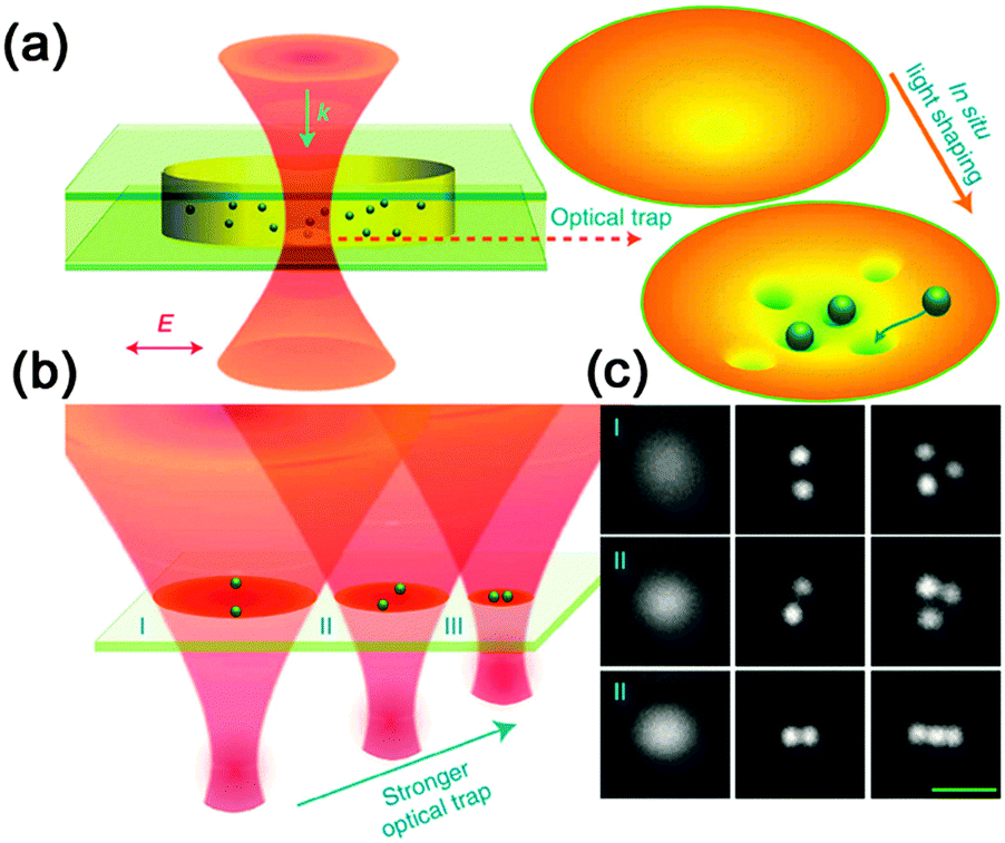 | ||
| Fig. 2 (a) Cooperating optical trapping and optical bonding for assembling arrays of NPs. (b) The trapping planes could be chosen by modulating the position of the focus. (c) Optical images of single, double and triple Ag NPs (100 nm) trapped in the different planes illustrated in (b). Scale bar is 1 μm. (Reproduced from ref. 85 with the permission of the Nature Publishing Group.) | ||
To increase the assembly efficiency, OT arrays could be achieved by employing a spatial light modulator (SLM) or multi-beam interference. Typically, Grier et al. applied a Hamamatsu SLM in front of the object telescope; in this way, they obtained hundreds of beams with a controllable phase.86 Through modulating their incidence directions and the degree of collimation, arrays of potential wells arose in the focus volume. Since the SLM could be totally controlled using a computer, the distribution of the potential wells could be flexibly designed for the subsequent trapping of colloidal particles. It is worth pointing out that the configuration of the colloidal particle assembly could be changed dynamically by tuning the SLM using pre-programed patterns. Based on these results, we could reach the conclusion that modulating the spatial light distribution is very useful for NP manipulation and multi-NP assembly.
3.2. Near-field OT
Traditional OT in micro/nanoscale manipulation and assembly shows obvious limits on accuracy. Firstly, due to the diffraction limit, it is hard to confine a large field gradient into a nanoscale volume, for instance, below 100 nm. Secondly, the Brownian motion should be taken into account if higher accuracy is desired. Typically, enhancing the beam power seems to be a solution to this issue, however, the ablation effect should be taken into account; thus the beam power could be enhanced within a certain range. Recently, near-field OT has been adopted to address these problems. An evanescent field of nanoscale optical devices might efficiently confine the trapping volumes in potential wells of subwavelength sizes.87,88 If suitable incident light were coupled into resonant devices, the gradient of the evanescent field would be enhanced greatly.89–92 LSPR excited among various metal structures was also applied for enhanced trapping.93–97 As compared with far-field OT, producing enhanced and subwavelength potential wells is a double advantage of near-field OT.Notably, an evanescent field of waveguides has been used for trapping particles. As a typical example, Hu et al. successfully delivered colloidal particles along waveguides in a microfluidic chip.98 The gradient force trapped the NPs and the scattering force was responsible for pushing them in the direction of the light. If the microfluid (a fluid that is geometrically constrained to a small, typically sub-millimeter, scale) in the chip channel and the light in the waveguide counter propagated, the scattering force could be offset by the pushing force of the microfluid; in this way, they could control the NPs to the desired positions. Nonetheless, the evanescent field of a single waveguide was usually weak and would decrease rapidly with the increase in distance, resulting in unstable trapping. Yang et al. designed a silicon slot waveguide for trapping NPs.99 The interactions between the two waveguides enhanced the gradient of light intensity, obtaining a powerful trapping force. Another device to enhance the evanescent field was a resonant ring.100 Depending on the trapping force and scattering force, colloidal particles would travel in a circle along the ring. However, the scattering force, which competed with the gradient force for stable trapping, severely disturbed the assembly of particles in these devices. Recently, Mandal et al. created photonic crystal resonators coupled with a bus waveguide.101 The NPs were delivered by the bus waveguide to the photonic crystal resonators. Because of the strong confinement of the optical field, the photonic crystal resonators caught the NPs from the bus waveguide through the strong lateral gradient force. So they achieved stable and stationary NP assembly. With the help of the microfluidic device, the NPs could be released back to the bus waveguide for further delivery when the light was turned off.
Similarly, Jaquay et al. introduced a beam to excite a resonant mode of a photonic crystal slab and got a periodical assembly of colloidal particles.102 In this work, resonance was a precondition for near-field OT. The quality factor Q of the resonant cavity was calculated to be ∼170 under suitable conditions, which meant that the photonic crystal slab confined strong wells for trapping particles. Interestingly, trapping was reversible; if the extent of resonance was reduced, for instance, by turning the wavelength of the incident beam away from resonance, or by reducing the laser power, the trapped particles would be released from the slab. Fig. 3b–d describe the process of the assembly and release of colloidal particles on the photonic crystal slab. Besides, the size and dielectric constant of the particles should also be taken into account. For example, when metal colloidal particles were trapped on the slab, they would assemble as a line due to the strong OB force.103 This phenomenon was quite different from polystyrene particles that assembled on a plane. Since the uniform distribution of the resonant cavity only led to the very simple assembly of the NPs (e.g., in lines or on a plane), more complex assemblies of the NPs would be achieved using the rational design of the distribution of these nanocavities.
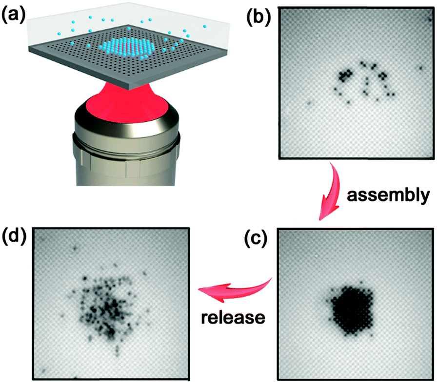 | ||
| Fig. 3 (a) The principle of resonant cavity aid assembly of 520 nm colloidal particles. (b–d) The process for the assembly and release of the particles by modulating the resonance of the microcavity. (Reproduced from ref. 102 with the permission of the American Chemical Society.) | ||
In addition to resonant microcavities, LSPR was also utilized to enhance the gradient force for OT. Particularly, with the rapid development of nanomanufacturing technologies, metallic nanostructures were successfully prepared for LSPR. For instance, Grigorenko et al. successfully fabricated nanopillar pair arrays using electron beam lithography for LSPR enhanced trapping,104 as shown in Fig. 4. The narrow nanogaps between the nanopillars strongly confined the electromagnetic field in small volumes, acting as deep potential wells with very small trapping volumes beyond the diffraction limit. The gradient forces arising here were thought to be several orders of magnitude higher than the traditional ones, whereby the precise assembly and manipulation of the NPs could be achieved, and the Brownian movement of the NPs could be effectively suppressed. Nevertheless, heat produced via LSPR might also bring a certain disturbance to OT. For instance, heat convection from both the lateral and vertical directions would push the trapping targets away. Additionally, the obviously risen temperature would accelerate the Brownian movement of the NPs. In this regard, the LSPR induced thermal effect should be suppressed for PDA. As a typical example, Wang et al. fabricated gold nanopillar arrays on gold and copper substrates that have high thermal conductivities. In this way, the heat generated via LSPR would be conducted into the substrate.105 Righini et al. reduced the density of metal structures to reduce the heat effect,106 while Kang et al. combined LSPR OT and thermodynamics for the larger area assembly of NPs.107 In their work, LSPR substrates would generate a wide distribution of nanogaps where strong gradients of electromagnetic fields were achieved for OT. Very interestingly, the LSPR induced heat effect has been used for enhancing the PDA process.
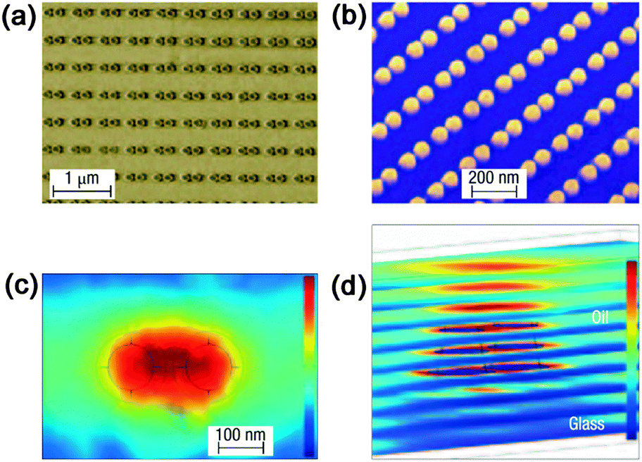 | ||
| Fig. 4 Electron micrographs of an array of nanopillar pairs, (a) overlook and (b) under a tilted angle. Every nanopillar was 90 nm in height. (c) Optical field intensity distribution of a plane about 200 nm above the substrate. (d) Different planes of optical field intensity distributions of a nanopillar pair, separated by 50 nm. (Reproduced from ref. 104 with the permission of the Nature Publishing Group.) | ||
With the rapid progress of modern micro/nanomanufacture technologies, near-field optics trapping that makes full use of the waveguide/micro-cavity and LSPR has been successfully developed for the controllable assembly of NPs. Unlike conventional OT, in the case of near-field optics, local optical fields could be enhanced by several orders of magnitude, which leads to great gradients of electromagnetic fields for NP trapping. However, near-field OT, which depends on structured substrates, also shows limitations in practical use, especially in the integration of NP assemblies, since a waveguide or LSPR structures should be fabricated beforehand for such an assembly.
4. FsL-PDA for the flexible assembly of NPs
Femtosecond laser direct writing (FsLDW) has been proven to enable the fabrication of 3D micronanostructures with high spatial resolution,108 since multi-photon absorption (MPA) induced photoreactions only occur within a small volume.109,110 Recently, FsLDW technology has also been used for the PDA of NPs towards flexible patterning.111,112 By moving the focus, the trapping potential wells would trap the NPs and induce assembly along the scanning tracks; in this way, various microstructures that consist of NP assemblies could be fabricated according to the preprogrammed patterns. As compared with the other PDAs introduced previously, FsL-PDA shows obvious advantages. First, a femtosecond laser has an ultra-short pulse, which is shorter than many relaxation processes, for instance, thermal relaxation. Therefore, the thermal relaxation effect could be well suppressed. In addition, the nonlinear absorption effect together with the threshold effect would lead to micronanostructures with high resolution, beyond the light diffraction limit. Moreover, since FsLDW enables 3D fabrication, the assembly of NPs through FsL-PDA permits flexible patterning on non-planar substrates. The FsL-PDA of NPs holds great promises for the flexible fabrication and integration of micro-nanodevices based on NPs.As a typical example, micropatterns based on semiconductor quantum dots (QDs) have been successfully prepared through FsL-PDA.113 Xu et al. assembled CdTe QDs into various micropatterns and further integrated the assemblies within a microfluidic device. Fig. 5a describes the principle of the FsL-PDA of QDs. Very interestingly, the quantum confinement effect was reserved, and the QDs did not grow into bulky materials after laser irradiation since thermal relaxation had been significantly suppressed. As shown in Fig. 5c, the absorption and luminescence spectra before and after the QDs had been treated using the femtosecond laser showed that the characters of the QDs remained to a large extent. The distinguishable shift was considered to be caused by a little decrease in the confinement effect, the loss of surface-capping ligands, and the dipole–dipole coupling interactions between the QDs in aggregates. The high resolution TEM image (Fig. 5d) provides direct evidence that the QDs aggregated together instead of growing into bulky crystals. Besides, the resultant QD assemblies were also proven to be conductive with strong reducibility. When they were exposed to Pb2+, an obvious increase in the resistivity was observed. Additionally, fluorescence was quenched. These properties make the QD assemblies very good sensors for the on-chip detection of heavy metal ions. In this work, FsL-PDA achieved a close-packed assembly of QDs on substrates without losing the quantum confinement effect. Moreover, the FsL-PDA of QDs is not limited to CdTe QDs, other semiconductor QDs could be assembled in a similar way.
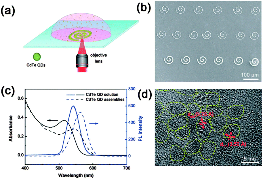 | ||
| Fig. 5 (a) The principle of the FsL-PDA of QDs. (b) Scanning electron microscopy (SEM) image of different widths of the circle structures made of close-packed QDs. (c) Absorption (black lines) and luminescence spectra (blue lines) of the QDs (solid lines) and QD assemblies (dashed lines). (d) High resolution transmission electron microscopy (TEM) image of the QD assembly sample, the yellow circles indicate individual nanocrystals. (Reproduced from ref. 113 with the permission of the Royal Society of Chemistry.) | ||
In fact, NPs at a Rayleigh size are quite suitable for FsL-PDA, for instance, Ag and Au NPs. As a typical example, Wang et al. assembled Ag NPs with an average particle size of ∼2.5 nm into various patterns via FsL-PDA technology (Fig. 6a).111 According to the computer-aided design (CAD) programs, it was easy to assemble Ag NPs into the desired micropatterns with a resolution as high as 190 nm. Moreover, by tuning the laser power or scanning times, silver lines of different widths could be obtained. By taking advantage of the controllable assembly, several 2D micro-patterns have been successfully fabricated. The magnified images showed that the silver NPs were close-packed aggregates (Fig. 6b). Being a precise and flexible craft, FsL-PDA is competent to assemble NPs into microfluidic chips as functional parts, such as electrodes with appropriate shapes and sizes for electrochemical analysis, microheaters for temperature control, and micropumps for directional delivery. In addition, FsL-PDA is compatible with traditional semiconductor crafts. A simple bottom gate field effect transistor based on a single multiwall carbon nanotube (MWCNT) has been successfully fabricated by combining traditional crafts and the FsL-PDA of Au NPs.112 Integrating a MWCNT into pre-existing devices seems impossible for other crafts, while in the case of FsL-PDA, the MWCNT could be connected to the source/drain electrodes by assembling conductive Au microwires. The whole procedure was carried out in atmosphere without complex vacuum equipment.
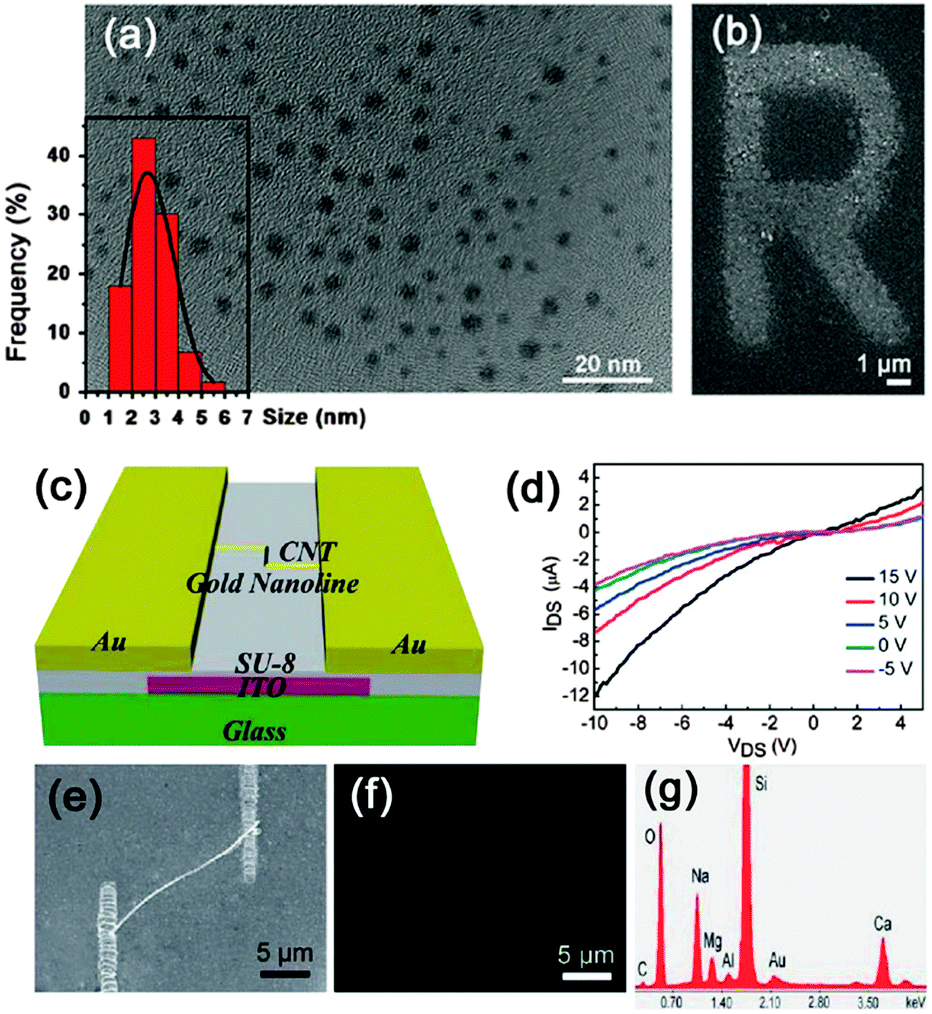 | ||
| Fig. 6 (a) Uniform Ag NPs used for FsL-PDA. Inset is the size distribution of the NPs. (b) An “R” letter assembled from Ag NPs. (c) Design for a MWCNT-FET fabricated via FsL-PDA. (d) Output characteristics and (e) SEM image of a MWCNT-FET. (f and g) Energy-dispersive X-ray (EDX) map and spectrum of the MWCNT-FET in (e). (Reproduced from ref. 111 and 112 with the permission of IOPscience and the Royal Society of Chemistry.) | ||
Generally, metal NPs used for FsL-PDA could be prepared beforehand. As introduced in the above-mentioned studies, NPs of Ag and Au have been patterned into various assemblies or fused together under high intensity irradiation. As an alternative choice, Ag NPs could also be directly synthesized within the laser focus. The in situ preparation of NPs using a femtosecond laser through a multiphoton absorption (MPA) induced photoreduction process has been reported for several years.114–117 The as-obtained silver NPs would be directly trapped for FsL-PDA. Cao et al. fabricated nanostructures by assembling silver NPs assisted with surfactants.118,119 To achieve smooth silver surfaces, the assembly process should be well controlled to avoid the growth of silver nuclei. As soon as silver atoms nucleated, they were covered by surfactants, which hindered the tiny NPs from growing any bigger. Increasing the concentration or the carbon chain length of the surfactant was effective to obtain the smooth morphology of the silver structures, even in 3D. Nevertheless, the presence of surfactants debased their electronic conductivity obviously, which immensely impeded their further applications in electronics. To solve this problem, Xu et al. chose trisodium citrate instead of surfactants to prepare the silver precursor and achieved conductive silver structures with high resolution.120 The resistivity of the silver microstructures is estimated to be 1.7 × 10⁷ Ωm, only ten times that of the bulk material. By integrating such silver structures within a microfluidic device, the silver patterns could act as an excellent microheater for localized temperature control. Taking advantage of the 3D feature of FsLDW, the silver microstructures could be fabricated continually on 3D substrates, providing the feasibility for integration of 3D electronics. Moreover, the high compatibility made FsL-PDA technology a promising craft for integrating conductive devices with given chips, for instance, microfluidic devices.
In the previous section, we discussed near-field OT for flexible PDA, in which metal structures on the substrates produced local optical fields to trap NPs. In the case of FsL-PDA, the near-field OT effect also exists. Briefly, the first layer of silver NPs assembled via FsL-PDA could be excited to generate LSPR which was able to enhance the gradient forces for further layer assembly.121 Generally, silver NPs in the first layer could be prepared through photoreduction of silver ions; then the as-formed Ag NPs were polarized under irradiation in the direction of laser polarization. At the endpoints of the dipoles, the local surface plasma that enhanced the trapping wells gathered; in this way, the NPs in solution tended to be assembled along the dipoles in the wells, forming nanoripple or nanoplate structures instead of smooth surfaces, as shown in Fig. 7a and b. Fig. 7c shows the schematic illustration of the principle of the whole assembly process. In addition to the near-field OT effect, the local surface plasma would also increase the chemical reactivity of the reduction reaction, which accelerated the growth of nanoplates significantly. After scanning for several layers, an array of silver nanoplates formed in the direction of laser polarization. And it was proven that the orientation of the silver nanoplates would be tuned by adjusting the direction of laser polarization, which further proved the formation mechanism of the silver nanoplates.
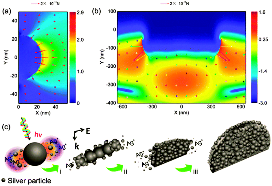 | ||
| Fig. 7 (a) E-field distribution of a 50 nm silver seed and the arrows represent the gradient forces attracting the silver atoms in the dipole of the silver seed. (b) E-field distribution of 300 nm ripples and the arrows represent the gradient forces attracting the silver atoms in the dipole of the silver ripple. The length of each arrow in (a) and (b) indicates the magnitude of the force. (c) Proposed mechanism for the formation of the silver nanoplates. (Reproduced from ref. 121 with the permission of the American Chemical Society.) | ||
The silver nanoplate structures prepared via FsL-PDA also showed a hierarchical roughness.121 Magnified SEM images showed that plenty of silver NPs decorated the surface of the vertical nanoplates. The hierarchical structures led to not only a large specific surface area, which contributed to chemical catalysis, but also very rough surfaces, which could be used for Surface Enhanced Raman Scattering (SERS) detection. In Xu's work, the enhancement factor of the SERS substrate prepared via FsL-PDA was estimated to be 1011. Actually, the ultrahigh enhancement factor could be explained by two points. Firstly, the nanoplates were fully covered with Ag NPs, which provided dense “hot spots” for SERS. Secondly, the vertical nanoplate arrays packed closely to each other in 3D, vastly increasing the active surfaces that enriched the probe molecules. To further demonstrate the excellent SERS activity, the signals were collected from different positions on the same substrate and the distinction among them was less than 5%.122 As a controllable and flexible craft, the desired shapes and locations of the SERS substrates could be integrated accurately into microfluidic chips. Besides, the Ag nanoplate arrays could also act as catalytic active sites for the reduction of 4-nitrophenol (4-NP) to 4-aminophenol (4-AP),123 as shown in Fig. 8. During the reaction, the SERS signals of 4-AP could be detected with increasing intensity, while the micro-region absorption spectra of 4-NP decreased gradually, indicating the conversion from 4-NP to 4-AP, as shown in Fig. 8b and c. After reaction for only 7 minutes, the conversion could reach ∼100%.
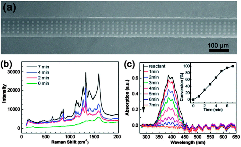 | ||
| Fig. 8 (a) A microchannel fully assembled with Ag clusters. (b) Raman spectra collected during the catalysis reaction. (c) Micro-region absorption spectra of the microfluids during the catalysis reaction. The inset of (c) is the kinetic study of the reaction. (Reproduced from ref. 123 with the permission of the Royal Society of Chemistry.) | ||
Taking advantage of the ultra-short laser pulses and the 3D processing capability, FsL-PDA has revealed great potential for the flexible patterning of NPs on any desired substrates (e.g., non-planar substrates). Additionally, the direct writing feature of femtosecond laser processing enables designable fabrication without the use of any masks. Owning to these unique advantages, FsL-PDA may find broad applications in the development of nanodevices.
5. Conclusions and future prospect
In addition to conventional assembly methods that were self-initiated, PDA makes use of external optical forces, such as the trapping force, pushing force, and pulling force. Since the optical forces are exerted by light, which could propagate freely in many media, PDA shows a series of unique advantages over conventional assembly technologies, for instance, non-contact manipulation, precise control and flexible patterning. In this review, we simply summarized the state-of-the-art of PDA technology, especially for NP assembly. Actually, in most cases, OT has been considered as the driving force for the PDA of NPs. The trapping mechanism for targets at a geometric optical (r ≫ λ) size and a Rayleigh (r ≪ λ) size has been introduced, in which the modulation of the potential well distributions is found to be an effective manner for NP trapping. When a suitable beam is chosen, objects with a feature size ranging from hundreds of microns to several nanometers might be manipulated. Generally, the potential wells produced by a laser beam could be considered as micro-tweezers, which can precisely control the assembly of NPs. As compared with some 2D assembly techniques that make use of the interaction between nanoparticles and substrates, PDA is much superior, since various NPs such as dielectric NPs, metal NPs, and QDs, could be manipulated and assembled without any complex chemical modification of both the NPs and the substrates. Moreover, with the help of near-field optical structures, trapping could be enhanced and the precision would be increased to the nanoscale. However, in the case of near-field OT, a waveguide device or plasmonic structures are generally necessary for the PDA of NPs, which more or less limits their wide application.Additionally, the FsL-PDA technology that assembles NPs through a direct writing manner shows distinct advantages due to the use of ultra-short laser pulses. In particular, the nonlinear optical effect contributes to the high resolution of the NP assemblies. Furthermore, the mask-free FsL-PDA technology enables the flexible patterning of NPs on various substrates, for example, non-planar substrates or even given devices. In this regard, FsL-PDA is compatible with device fabrication and integration, revealing great potential to bridge the gap between nanomaterials and functional devices. However, since a single beam was used for the whole assembly process, FsL-PDA suffered from a relative low efficiency. Nevertheless, this situation would be improved by using a spatial light modulator (SLM), for instance, multiple beam trapping could significantly increase the efficiency, and form more complex NP configurations.124,125 Currently, it is still challenging for FsL-PDA to make 3D assemblies of NPs in a controlled manner, despite the fact that FsLDW is capable of 3D photopolymerization. A possible reason would be the disturbance of LSPR with respect to Ag/Au NPs or the low concentration of NPs in the focus volume. As discussed in this paper, the formation of Ag or Au structures would lead to LSPR which governs the further assembly of the NPs; as a result, 3D metallic microstructures with perfect morphologies are almost impossible to achieve using FsL-PDA. This situation would be improved in the case of other NPs. However, to ensure the transmittance of the laser beam, the concentration of the NPs should not be too high. In the focal volume, there are not enough NPs that could be used as building blocks to construct the 3D structures. This seems to be a contradiction. Unless and until enough NPs could be delivered to the focal volume, a 3D assembly of NPs via FsL-PDA would be expected.
At present, the PDA of NPs is still at an early stage. Most of the research efforts have been devoted to the manipulation of NPs. In fact, as a bottom-up craft, PDA also holds great promises for the flexible patterning and structuring of nanodevices by assembling various NPs. Moreover, in addition to NPs, PDA might also find applications in the assembly of biomaterials, such as cells and proteins, revealing great potential for tissue engineering. With the rapid development of nanotechnology, we deem that the PDA of NPs will enable the flexible assembly of NPs towards the development of functional devices based on nanomaterials.
Acknowledgements
The authors would like to acknowledge the financial support from Natural Science Foundation of China (NSFC) and National Basic Research Program of China under grants No. 61522503, 2011CB013000, 2014CB921302, 61435005, 61376123. We thank Wei Wang for helpful discussion.Notes and references
- N. C. Anheier, Nature, 2015, 523, 39–40 CrossRef CAS PubMed.
- H. Gao, Y. W. Hu, Y. Xuan, J. Li, Y. L. Yang, R. V. Martinez, C. Y. Li, J. Luo, M. H. Qi and G. J. Cheng, Science, 2014, 346, 1352–1356 CrossRef CAS PubMed.
- M. I. Stockman, Science, 2015, 348, 287–288 CrossRef CAS PubMed.
- K. Uenoab and H. Misawa, Phys. Chem. Chem. Phys., 2013, 15, 4093–4099 RSC.
- Q. Sun, K. Ueno, H. Yu, A. Kubo, Y. Matsuo and H. Misawa, Light: Sci. Appl., 2013, 2, e118 CrossRef CAS.
- Q. M. Ji, J. P. Hillab and K. Ariga, J. Mater. Chem. A, 2013, 1, 3600–3606 CAS.
- L. K. Shrestha, M. Sathish, J. P. Hill, K. Miyazawa, T. Tsuruoka, N. M. Sanchez-Ballester, I. Honma, Q. M. Ji and K. Ariga, J. Mater. Chem. C, 2013, 1, 1174–1181 RSC.
- E. Abdullayev, K. Sakakibara, K. Okamoto, W. B. Wei, K. Ariga and Y. Lvov, ACS Appl. Mater. Interfaces, 2011, 3, 4040–4046 CAS.
- Y. B. Lee, S. H. Lee, S. Y. Park, C. J. Park, K. S. Lee, J. Y. Kim and J. S. Joo, Synth. Met., 2014, 187, 130–135 CrossRef CAS.
- Y. Liao, J. X. Song, E. Li, Y. Luo, Y. L. Shen, D. P. Chen, Y. Cheng, Z. Z. Xu, K. Sugiokad and K. Midorikawa, Lab Chip, 2012, 12, 746–749 RSC.
- Y. Liao, Y. Cheng, C. N. Liu, J. X. Song, F. He, Y. L. Shen, D. P. Chen, Z. Z. Xu, Z. C. Fan, X. B. Wei, K. Sugiokac and K. Midorikawa, Lab Chip, 2013, 13, 1626–1631 RSC.
- J. J. Park, X. Bulliard, J. M. Lee, J. Hur, K. Im, J. M. Kim, P. Prabhakaran, N. Cho, K. S. Lee, S. Y. Min, T. W. Lee, S. Yong and D. Y. Yang, Adv. Funct. Mater., 2010, 20, 2296–2302 CrossRef CAS.
- Z. B. Sun, X. Z. Dong, W. Q. Chen, S. Nakanishi, X. M. Duan and S. Kawata, Adv. Mater., 2008, 20, 914–919 CrossRef CAS.
- A. Spende, N. Sobel, M. Lukas, R. Zierold, J. C. Riedl, L. Gura, I. Schubert, J. M. M. Moreno, K. Nielsch, B. Stühn, C. Hess, C. Trautmann and M. E. Toimil-Molares, Nanotechnology, 2015, 26, 335301 CrossRef PubMed.
- M. I. Schukfeh, K. Storm, A. Hansen, C. Thelander, P. Hinze, A. Beyer, T. Weimann, L. Samuelson and M. Tornow, Nanotechnology, 2014, 25, 465306 CrossRef CAS PubMed.
- C. B. Murray and C. R. Kagan, Annu. Rev. Mater. Sci., 2000, 30, 545–610 CrossRef CAS.
- C. F. Guo, T. Y. Sun, F. Cao, Q. Liu and Z. F. Ren, Light: Sci. Appl., 2014, 3, e161 CrossRef.
- Y. H. Su, Y. F. Ke, S. L. Cai and Q. Y. Yao, Light: Sci. Appl., 2012, 1, e14 CrossRef.
- J. Liu, Y. Liu, N. Y. Liu, Y. Z. Han, X. Zhang, H. Huang, Y. Lifshitz, S. T. Lee, J. Zhong and Z. H. Kang, Science, 2015, 347, 970–974 CrossRef CAS PubMed.
- X. M. Gu, Z. H. Sun, S. C. Wu, W. Qi, H. H. Wang, X. Z. Xu and D. S. Su, Chem. Commun., 2013, 49, 10088–10090 RSC.
- X. M. Gu, W. Qi, X. Z. Xu, Z. H. Sun, L. Y. Zhang, W. Liu, X. L. Pan and D. S. Su, Nanoscale, 2014, 6, 6609–6616 RSC.
- S. X. Zhang, N. Wang, Y. M. Niu and C. Q. Sun, Sens. Actuators, B, 2005, 109, 367–374 CrossRef CAS.
- N. A. Luechinger, E. K. Athanassiou and W. J. Stark, Nanotechnology, 2008, 19, 445201 CrossRef PubMed.
- S. H. Ko, I. Park, H. Pan, C. P. Grigoropoulos, A. P. Pisano, C. K. Luscombe and J. M. J. Frechet, Nano Lett., 2007, 7, 1869–1877 CrossRef CAS PubMed.
- W. Q. Kong, H. Li, J. Liu, S. J. Guo, Y. Z. Han, H. Huang, Y. Liu and Z. H. Kang, J. Mater. Chem. B, 2015, 3, 1198–1203 RSC.
- S. Chernousova and M. Epple, Angew. Chem., Int. Ed., 2013, 52, 1636–1653 CrossRef CAS PubMed.
- D. M. Eby, N. M. Schaeublin, K. E. Farrington, S. M. Hussain and G. R. Johnson, ACS Nano, 2009, 3, 984–994 CrossRef CAS PubMed.
- B. Su, C. Zhang, S. R. Chen, X. Y. Zhang, L. F. Chen, Y. C. Wu, Y. W. Nie, X. N. Kan, Y. L. Song and L. Jiang, Adv. Mater., 2014, 26, 2501–2507 CrossRef CAS PubMed.
- E. U. Kim, K. J. Baeg, Y. Y. Noh, D. Y. Kim, T. Lee, I. Park and G. Y. Jung, Nanotechnology, 2009, 20, 355302 CrossRef PubMed.
- Z. H. Nie, A. Petukhova and E. Kumacheva, Nat. Nanotechnol., 2009, 5, 15–25 CrossRef PubMed.
- M. H. Lash, M. V. Fedorchak, J. J. McCarthy and S. R. Little, Soft Matter, 2015, 11, 5597–5609 RSC.
- M. Geissler and Y. N. Xia, Adv. Mater., 2004, 16, 1249–1269 CrossRef CAS.
- V. Pachauri, C. Subramaniam and T. Pradeep, Chem. Phys. Lett., 2006, 423, 240–246 CrossRef CAS.
- G. F. S. Andrade, M. K. Fan and A. G. Brolo, Biosens. Bioelectron., 2010, 25, 2270–2275 CrossRef CAS PubMed.
- Y. L. Wang, H. J. Chen, S. J. Dong and E. K. Wang, J. Raman Spectrosc., 2007, 38, 515–521 CrossRef CAS.
- X. L. Li, J. H. Zhang, W. Q. Xu, H. Y. Jia, X. Wang, B. Yang, B. Zhao, B. F. Li and Y. Ozaki, Langmuir, 2003, 19, 4285–4290 CrossRef CAS.
- X. Che, R. Yuan, Y. Q. Chai, J. J. Li, Z. J. Song and J. F. Wan, J. Colloid Interface Sci., 2010, 345, 174–180 CrossRef CAS PubMed.
- Y. Z. Zhou, J. Yang, X. N. Cheng, N. Zhao, L. Sun, H. B. Sun and D. Li, Carbon, 2012, 50, 4343–4350 CrossRef CAS.
- J. W. Liu, S. Y. Zhang, H. Qi, W. C. Wen and S. H. Yu, Small, 2012, 8, 2412–2420 CrossRef CAS PubMed.
- J. X. Huang, A. R. Tao, S. Connor, R. R. He and P. D. Yang, Nano Lett., 2006, 6, 524–529 CrossRef CAS PubMed.
- M. L. Curri, R. Comparelli, M. Striccolia and A. Agostiano, Phys. Chem. Chem. Phys., 2010, 12, 11197–11207 RSC.
- L. D. Michele and E. Eiser, Phys. Chem. Chem. Phys., 2013, 15, 3115–3129 RSC.
- S. J. Tan, M. J. Campolongo, D. Luo and W. Cheng, Nat. Nanotechnol., 2011, 6, 268–276 CrossRef CAS PubMed.
- S. J. Barrow, A. M. Funston, X. Z. Wei and P. Mulvaney, Nano Today, 2013, 8, 138–167 CrossRef CAS.
- G. Wei, L. Wang, Z. G. Liu, Y. H. Song, L. L. Sun, T. Yang and Z. Li, J. Phys. Chem. B, 2005, 109, 23941–23947 CrossRef CAS PubMed.
- B. D. Korth, P. Keng, I. Shim, S. E. Bowles, C. B. Tang, T. Kowalewski, K. W. Nebesny and J. Pyun, J. Am. Chem. Soc., 2006, 128, 6562–6563 CrossRef CAS PubMed.
- K. D. Hermanson, S. O. Lumsdon, J. P. Williams, E. W. Kaler and O. D. Velev, Science, 2001, 294, 1082–1086 CrossRef CAS PubMed.
- R. Sheparovych, Y. Sahoo, M. Motornov, S. M. Wang, H. Luo, P. N. Prasad, I. Sokolov and S. Minko, Chem. Mater., 2006, 18, 591–593 CrossRef CAS.
- O. D. Velev and K. H. Bhatt, Soft Matter, 2006, 2, 738–750 RSC.
- J. J. Park, P. Prabhakaran, K. K. Jang, Y. G. Lee, J. Lee, K. H. Lee, J. Hur, J. M. Kim, N. Cho, Y. Son, D. Y. Yang and K. S. Lee, Nano Lett., 2010, 10, 2310–2317 CrossRef CAS PubMed.
- K. K. Jang, P. Prabhakaran, D. Chandran, J.-J. Park and K.-S. Lee, Opt. Mater. Express, 2012, 2, 519–525 CrossRef CAS.
- Z. H. Wang, Y. M. Liu, P. Tao, Q. C. Shen, N. Yi, F. Y. Zhang, Q. L. Liu, C. Y. Song, D. Zhang, W. Shang and T. Deng, Small, 2014, 10, 3234–3239 CrossRef CAS PubMed.
- V. Santhanam and R. P. Andres, Nano Lett., 2004, 4, 41–44 CrossRef CAS.
- J. Y. Chen, P. Mela, M. Moller and M. C. Lensen, ACS Nano, 2009, 3, 1451–1456 CrossRef CAS PubMed.
- B. Y. Ahn, E. B. Duoss, M. J. Motala, X. Y. Guo, S. I. Park, Y. J. Xiong, J. Yoon, R. G. Nuzzo, J. A. Rogers and J. A. Lewis, Science, 2009, 323, 1590–1593 CrossRef CAS PubMed.
- W. F. Shen, X. P. Zhang, Q. J. Huang, Q. S. Xu and W. J. Song, Nanoscale, 2014, 6, 1622 RSC.
- S. W. Lee, G. Jo, T. Lee and Y. G. Lee, Opt. Express, 2009, 17, 17491–17501 CrossRef CAS PubMed.
- J. Do, R. Schreiber, A. A. Lutich, T. Liedl, J. Rodríguez-Fernandez and J. Feldmann, Nano Lett., 2012, 12, 5008–5013 CrossRef CAS PubMed.
- J. H. J. Huissteede, V. Subramaniam and M. Bennink, Microsc. Res. Tech., 2007, 70, 26–33 CrossRef PubMed.
- H. Hwang, D. Han, Y. Oh, Y. Cho, K. H. Jeonga and J. K. Park, Lab Chip, 2011, 11, 2518–2525 RSC.
- L. Jauffred, A. C. Richardson and L. B. Oddershede, Nano Lett., 2008, 8, 3376–3380 CrossRef CAS PubMed.
- O. M. Maragò, P. H. Jones, P. G. Gucciardi, G. Volpe and A. C. Ferrari, Nat. Nanotechnol., 2013, 8, 807–819 CrossRef PubMed.
- M. Daly, M. Sergides and S. N. Chormaic, Laser Photonics Rev., 2015, 9, 309–329 CrossRef CAS.
- M. Gu, H. C. Bao, X. S. Gan, N. Stokes and J. Z. Wu, Light: Sci. Appl., 2014, 3, e126 CrossRef CAS.
- A. Lehmuskero, P. Johansson, H. Rubinsztein-Dunlop, L. Tong and M. Kall, ACS Nano, 2015, 9, 3453–3469 CrossRef CAS PubMed.
- A. Jonas and P. Zemanek, Electrophoresis, 2008, 29, 4813–4851 CrossRef CAS PubMed.
- K. Svoboda and S. M. Block, Opt. Lett., 1994, 19, 930–932 CrossRef CAS PubMed.
- K. dholakia and T. Čižmár, Nat. Photonics, 2011, 5, 335–342 CrossRef CAS.
- T. Cizmar, L. C. D. Romero, K. Dholakia and D. L. Andrews, J. Phys. B: At., Mol. Opt. Phys., 2010, 43, 102001 CrossRef.
- G. Brugger, L. S. Froufe-Perez, F. Scheffold and J. J. Saenz, Nat. Commun., 2015, 6, 7460 CrossRef CAS PubMed.
- A. Ashkin, J. M. Dziedzic, J. E. Bjorkholm and S. Chu, Opt. Lett., 1986, 11, 288–290 CrossRef CAS PubMed.
- K. Dholakia and P. Reece, Nano Today, 2006, 1, 18–27 CrossRef.
- D. G. Grier, Nature, 2003, 424, 810–816 CrossRef CAS PubMed.
- D. Erickson, X. Serey, Y. F. Chenac and S. Mandal, Lab Chip, 2011, 11, 995–1009 RSC.
- K. Dholakia and P. Zemánek, Rev. Mod. Phys., 2010, 82, 1767–1791 CrossRef.
- J. Ng, Z. F. Lin, C. T. Chan and P. Sheng, Phys. Rev. B: Condens. Matter Mater. Phys., 2005, 72, 085130 CrossRef.
- F. Svedberg, Z. P. Li, H. X. Xu and M. Kall, Nano Lett., 2006, 6, 2639–2641 CrossRef CAS PubMed.
- Z. J. Yan, U. Manna, W. Qin, A. Camire, P. Guyot-Sionnest and N. F. Scherer, J. Phys. Chem. Lett., 2013, 4, 2630–2636 CrossRef CAS.
- Z. J. Yan, R. A. Shah, G. Chado, S. K. Gray, M. Pelton and N. F. Scherer, ACS Nano, 2013, 7, 1790–1802 CrossRef CAS PubMed.
- C. D. Mellor and C. D. Bain, ChemPhysChem, 2006, 7, 329–332 CrossRef CAS PubMed.
- C. D. Mellor, Opt. Express, 2006, 14, 10079–10088 CrossRef PubMed.
- V. Demergis and E. L. Florin, Nano Lett., 2012, 12, 5756–5760 CrossRef CAS PubMed.
- J. Chen, J. Ng, Z. F. Lin and C. T. Chan, Nat. Photonics, 2011, 5, 531–534 CrossRef CAS.
- M. J. Guffey and N. F. Scherer, Nano Lett., 2010, 10, 4302–4308 CrossRef CAS PubMed.
- Z. J. Yan, S. K. Gray and N. F. Scherer, Nat. Commun., 2014, 5, 3751 CAS.
- J. E. Curtis, B. A. Koss and D. G. Grier, Opt. Commun., 2002, 207, 169–175 CrossRef CAS.
- X. D. Yang, Y. M. Liu, R. F. Oulton, X. B. Yin and X. Zhang, Nano Lett., 2011, 11, 321–328 CrossRef CAS PubMed.
- J. Xu, W. P. Zang and J. G. Tian, Opt. Express, 2015, 23, 4195–4205 CrossRef PubMed.
- C. A. Mejia, A. Dutt and M. L. Povinelli, Opt. Express, 2011, 19, 11422–11428 CrossRef PubMed.
- Y. Gong, C. L. Zhang, Q. F. Liu, Y. Wu, H. J. Wu, Y. J. Rao and G. D. Peng, Opt. Express, 2015, 23, 3762–3769 CrossRef PubMed.
- C. A. Mejia, N. F. Huang and M. L. Povinelli, Opt. Lett., 2012, 17, 3690–3692 CrossRef PubMed.
- T. Wang, M. z. Ke, S. J. Xu, J. h. Feng, C. Y. Qiu and Z. Y. Liu, Appl. Phys. Lett., 2015, 106, 163504 CrossRef.
- M. L. Juan, M. Righini and R. Quidant, Nat. Photonics, 2011, 5, 349–356 CrossRef CAS.
- J. S. Huang and Y. T. Yang, Nanomaterials, 2015, 5, 1048–1065 CrossRef CAS.
- T. Shoji and Y. Tsuboi, J. Phys. Chem. Lett., 2014, 5, 2957–2967 CrossRef CAS PubMed.
- K. Wang, E. Schonbrun and K. B. Crozier, Nano Lett., 2009, 9, 2623–2629 CrossRef CAS PubMed.
- L. Huang, S. J. Maerkl and O. J. F. Martin, Opt. Express, 2009, 17, 6018–6024 CrossRef CAS PubMed.
- Y. J. Hu, Y. Li, Y. H. Deng and P. Peng, AIP Adv., 2015, 5, 037126 CrossRef.
- A. H. J. Yang, S. D. Moore, B. S. Schmidt, M. Klug, M. Lipson and D. Erickson, Nature, 2009, 457, 71–75 CrossRef CAS PubMed.
- S. Y. Lin, E. Schonbrun and K. Crozier, Nano Lett., 2010, 10, 2408–2411 CrossRef CAS PubMed.
- S. Mandal, X. Serey and D. Erickson, Nano Lett., 2010, 10, 99–104 CrossRef CAS PubMed.
- E. Jaquay, L. J. Martínez, C. A. Mejia and M. L. Povinelli, Nano Lett., 2013, 13, 2290–2294 CrossRef CAS PubMed.
- E. Jaquay, L. J. Martínez, N. F. Huang, C. A. Mejia, D. Sarkar and M. L. Povinelli, Nano Lett., 2014, 14, 5184–5188 CrossRef CAS PubMed.
- A. N. Grigorenko, N. W. Roberts, M. R. Dickinson and Y. Zhang, Nat. Photonics, 2008, 2, 365–370 CrossRef CAS.
- K. Wang, E. Schonbrun, P. Steinvurzel and K. B. Crozier, Nat. Commun., 2011, 2, 469 CrossRef PubMed.
- M. Righini, P. Ghenuche, S. Cherukulappurath, V. Myroshnychenko, F. J. GarcıadeAbajo and R. Quidant, Nano Lett., 2009, 9, 3387–3391 CrossRef CAS PubMed.
- Z. W. Kang, J. J. Chen, S. Y. Wu, K. Chen, S. K. Kong, K. T. Yong and H. P. Ho, Sci. Rep., 2015, 5, 9978 CrossRef CAS PubMed.
- S. Kawata, H. B. Sun, T. Tanaka and K. Takada, Nature, 2001, 412, 697–698 CrossRef CAS PubMed.
- Y. L. Zhang, Q. D. Chen, H. Xia and H. B. Sun, Nano Today, 2010, 5, 435–448 CrossRef CAS.
- B. B. Xu, Y. L. Zhang, H. Xia, W. F. Dong, H. Ding and H. B. Sun, Lab Chip, 2013, 13, 1677–1690 RSC.
- H. Wang, S. Liu, Y. L. Zhang, J. N. Wang, L. Wang, H. Xia, Q. D. Chen, H. Ding and H. B. Sun, Sci. Technol. Adv. Mater., 2015, 16, 024805 CrossRef.
- B. B. Xu, R. Zhang, H. Wang, X. Q. Liu, L. Wang, Z. C. Ma, Q. D. Chen, X. Z. Xiao, B. Han and H. B. Sun, Nanoscale, 2012, 4, 6955–6958 RSC.
- B. B. Xu, Y. L. Zhang, R. Zhang, L. Wang, X. Z. Xiao, H. Xia, Q. D. Chen and H. B. Sun, J. Mater. Chem. C, 2013, 1, 4699–4704 RSC.
- F. Stellacci, C. A. Bauer, T. Meyer-Friedrichsen, W. Wenseleers, V. Alain, S. M. Kuebler, S. J. K. Pond, Y. D. Zhang, S. R. Marder and J. W. Perry, Adv. Mater., 2002, 14, 194–198 CrossRef CAS.
- C. N. LaFratta, D. Lim, K. O’Malley, T. Baldacchini and J. T. Fourkas, Chem. Mater., 2006, 18, 2038–2042 CrossRef CAS.
- J. W. Wang, R. C. Y. Auyeung, H. Kim, N. A. Charipar and A. Piqué, Adv. Mater., 2010, 22, 4462–4466 CrossRef CAS PubMed.
- W. E. Lu, Y. L. Zhang, M. L. Zheng, Y. P. Jia, J. Liu, X. Z. Dong, Z. S. Zhao, C. B. Li, Y. Xia, T. C. Ye and X. M. Duan, Opt. Mater. Express, 2013, 3, 1660–1673 CrossRef.
- Y. Y. Cao, N. Takeyasu, T. Tanaka, X. M. Duan and S. Kawata, Small, 2009, 5, 1144–1148 CAS.
- Y. Y. Cao, X. Z. Dong, N. Takeyasu, T. Tanaka, Z. S. Zhao, X. M. Duan and S. Kawata, Appl. Phys. A: Mater. Sci. Process., 2009, 96, 453–458 CrossRef CAS.
- B. B. Xu, H. Xia, L. G. Niu, Y. L. Zhang, K. Sun, Q. D. Chen, Y. Xu, Z. Q. Lv, Z. H. Li, H. Misawa and H. B. Sun, Small, 2010, 6, 1762–1766 CrossRef CAS PubMed.
- B. B. Xu, L. Wang, Z. C. Ma, R. Zhang, Q. D. Chen, C. Lv, B. Han, X. Z. Xiao, X. L. Zhang, Y. L. Zhang, K. Ueno, H. Misawa and H. B. Sun, ACS Nano, 2014, 8, 6682–6692 CrossRef CAS PubMed.
- B. B. Xu, Z. C. Ma, L. Wang, R. Zhang, L. G. Niu, Z. Yang, Y. L. Zhang, W. H. Zheng, B. Zhao, Y. Xu, Q. D. Chen, H. Xia and H. B. Sun, Lab Chip, 2011, 11, 3347–3351 RSC.
- B. B. Xu, R. Zhang, X. Q. Liu, H. Wang, Y. L. Zhang, H. B. Jiang, L. Wang, Z. C. Ma, J. F. Ku, F. S. Xiao and H. B. Sun, Chem. Commun., 2012, 48, 1680–1682 RSC.
- J. I. Kato, N. Takeyasu, Y. Adachi, H. B. Sun and S. Kawata, Appl. Phys. Lett., 2005, 86, 044102 CrossRef.
- X. Z. Dong, Z. S. Zhao and X. M. Duan, Appl. Phys. Lett., 2007, 91, 124103 CrossRef.
| This journal is © The Royal Society of Chemistry 2016 |