
Fermi level, work function and vacuum level
Antoine
Kahn
Department of Electrical Engineering, Princeton University, Princeton, NJ 08544, USA. E-mail: kahn@princeton.edu
First published on 13th October 2015
Abstract
Electronic levels and energies of a solid, such as Fermi level, vacuum level, work function, ionization energy or electron affinity, are of paramount importance for the control of device behavior, charge carrier injection and transport. These levels and quantities, however, depend sensitively on the structure and surface morphology and chemical composition of the solid. A small amount of contaminants on a metal surface, or a shift in molecular orientation at the surface of an organic semiconductor, can change work function and vacuum level position by a large fraction of an electron-volt, and significantly impact the electronic structure of interfaces. The goal of this brief focus article is to provide definitions of key concepts and review simple mechanisms that affect these fundamental quantities.
Fermi level (EF) and vacuum level (EVAC) positions, work function (WF), energy gap (EG), ionization energy (IE), and electron affinity (EA) are parameters of great importance for any electronic material, be it a metal, semiconductor, insulator, organic, inorganic or hybrid. To a large extent, these parameters are key ingredients that define the electronic structure of all interfaces between a material and the outside world, and control processes of charge exchange and transport across interfaces in all electronic devices. However, they are also subject to significant variations between samples of the same material due to a multiplicity of internal and external factors ranging from purity of material (doped or undoped) to structure (surface crystallographic orientation) and morphology (surface roughness), processing history and surface composition (clean vs. contaminated). A thin film of polycrystalline gold typically exhibits a WF of 4.4–4.7 eV when exposed to ambient atmosphere, 5.0–5.1 eV when atomically clean and ordered under ultra-high vacuum, and up to 5.3–5.4 eV when sputter-cleaned under, for example, argon-ion bombardment! One must therefore always be well aware of the preparation conditions and environmental history of a film or surface when reporting on its surface-related properties.
To clarify these parameters and the various mechanisms that control them, consider the energy diagram of the surface region of a semiconductor in Fig. 1. For simplicity, the semiconductor is represented with flat bands near the surface, a condition that assumes no net charge accumulation at or near the surface. Although rarely encountered with inorganic semiconductors because of charges trapped in dangling bond-derived surface gap states, flat bands are often observed with molecular and polymer semiconductor surfaces, as these materials generally do not exhibit dangling bonds. The electron and hole single-particle transport levels in the inorganic semiconductor are the conduction band minimum (CBM) and valence band maximum (VBM), respectively. Their equivalent in an organic semiconductor are the lowest unoccupied and highest occupied molecular orbitals (LUMO, HOMO), respectively. We stress that, in the strict sense of the term, LUMO and HOMO should denote the unoccupied and occupied frontier levels of the neutral ground-state molecule, respectively. In this focus article, we use these terms in the way that has become standard among device physicists to represent the single-particle level of the electron or hole on the ionized molecule, respectively. Although the distinction is important to make, in particular for molecular solids, LUMO and HOMO are uniformly used in the literature to describe single-particle injection in, and transport through, organic semiconductors.
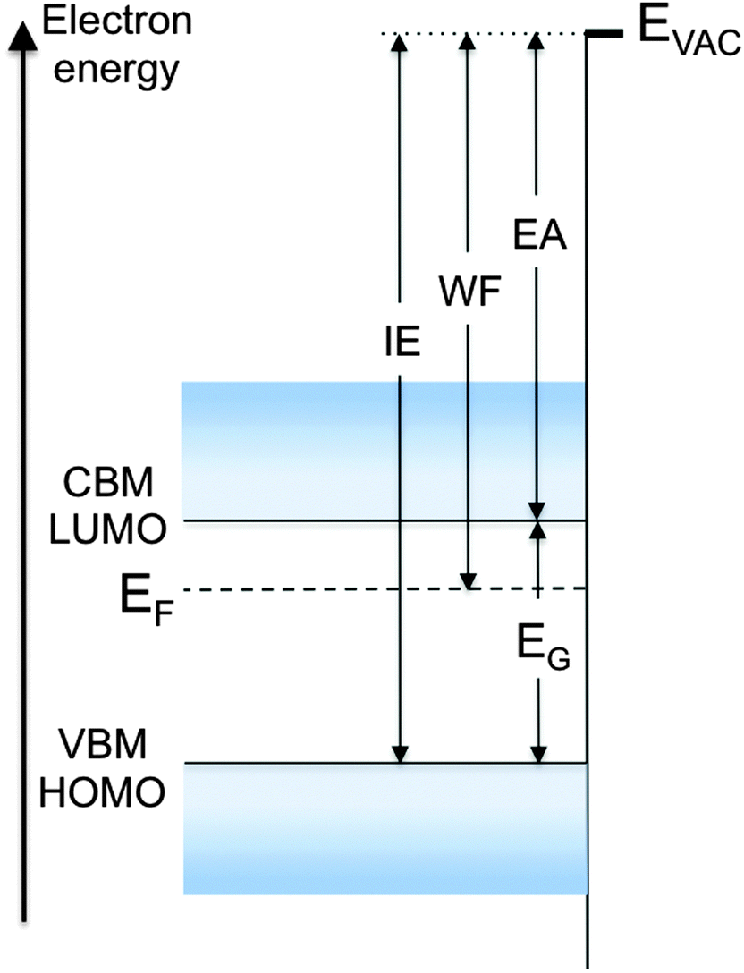 | ||
| Fig. 1 Energy diagram of a semiconductor with flat bands to the surface. Band edges (CBM/LUMO and VBM/HOMO), vacuum level EVAC, work function WF, energy gap EG, ionization energy IE and electron affinity EA are defined. | ||
The single-particle energy gap (EG), also called transport gap, is the energy difference between these levels (Fig. 1). EG and the single-particle levels, i.e. the lowest energy levels of the uncorrelated electron and hole, are central to the definition of all carrier injection and extraction barriers at metal/semiconductor and semiconductor/semiconductor heterojunctions. Note that for organic semiconductors in particular, EG must be distinguished from, and is generally significantly larger than, the optical gap of the material, EOPT, which corresponds to the excitation via photon absorption of the lowest energy electron–hole bound pair, or exciton. This topic was recently reviewed by Brédas in this very journal,1 and will not be revisited here.
Electrons are naturally bound to the solid. At the surface of the material, they are prevented to escape (to the vacuum) by an energy barrier that culminates at the vacuum level (EVAC). The standard definition of EVAC is the energy level of an electron positioned at rest within a “few nanometers” outside the solid, i.e. with zero kinetic energy with respect to the sample surface. The “few nanometer” distance is relatively loosely defined and corresponds to a distance sufficient for the electron to experience the full impact of the surface dipole (see below). Also known as the local vacuum level, EVAC is strongly influenced by the nature of the surface, as will be explained later. It is to be distinguished from the vacuum level at infinity (EVAC(∞)), which corresponds to the energy of an electron at rest far away from any solid surface. The latter has only theoretical implications, and is of no importance for the present discussion. More on the distinction between EVAC and EVAC(∞) can be found in Cahen et al.2
In the semiconductor represented in Fig. 1, neglecting the few electrons that might be present at the CBM or LUMO level as a result of doping or thermal excitation, the electrons closest in energy to EVAC are those at the VBM or HOMO level. The energy difference between EVAC and this level is therefore the minimum energy necessary to remove an electron from the system, and is known as the ionization energy (IE), defined here as a positive quantity. Conversely, neglecting the few holes that might be present at the VBM or HOMO level, the energy gained by dropping an electron from the vacuum level to the lowest unoccupied state, i.e. the CBM or LUMO, is the electron affinity (EA) of the solid, also defined here as a positive quantity.3 Typical semiconductors of interest in inorganic or organic electronics have EAs and IEs in the range of 2–4 eV and 4.5–6.5 eV, respectively. Values often diverge from these ranges for special-purpose materials, for example molecular dopants, which are designed to be either strong electron acceptors with large EA (>5.0 eV, p-dopant) or strong electron donors with low IE (<3.5 eV, n-dopant).
The local vacuum level EVAC is central to the definition and values of all parameters described in Fig. 1. We now look at the factors that contribute to its position and, as a consequence, to the value of the work function WF. The latter is defined as the energy necessary to remove an electron originally at the Fermi level (EF) deep inside the material and place it at rest at a point in free space just outside the surface, i.e. at EVAC. In a metal, EF marks the boundary between occupied and unoccupied states in a continuum of states, formally making IE and EA equal to the work function WF of the material. On the other hand, there are generally no states, and thus no electrons, at the Fermi level in a non-degenerate semiconductor, and WF in these materials takes on a statistical value that falls somewhere between IE and EA (Fig. 1). In a semiconductor, WF directly depends on the position of EVAC and on EF, which in turns depends on the density of states, temperature, carrier density and doping concentration in the material. WF is determined quantitatively via photoemission spectroscopy, which provides absolute measurements of both EF and EVAC positions (see below).
In a sense, the work function WF = EVAC − EF represents the energy barrier to free space that prevents an electron at the Fermi level from escaping the solid. This barrier, which culminates at EVAC, consists of two components, a bulk component and a surface component. WF is measured as the combination of the two components, which cannot be experimentally separated. The dominant one, i.e., the bulk component, corresponds to the chemical potential that derives from the electronic density and density of states in the solid. Its calculation involves the determination of the difference in energy between the N and N − 1 electron system. The surface component, also known as surface dipole component, corresponds to an additional potential step (positive or negative) that originates with a redistribution of charges at the surface of the solid. This component is inherent to the surface of the solid and exists only at the solid–vacuum interface. It is an integral constituent of WF and EVAC, two quantities that take meaning at, and only at, the surface of the solid. By extension, and according to the definitions of IE and EA given above, the ionization energy and electron affinity of the solid are defined at, and only at, the surface of the material.
The redistribution of charges at the surface of a material, which gives rise to the surface dipole, takes on several possible mechanisms. The generic mechanism for metal surfaces is the “spill out” of electron into vacuum. Deep in the metal, the electron density along the z direction perpendicular to the surface is constant (at least in a simple jellium-type model), but as the lattice abruptly terminates at the surface, electrons tunnel out the solid over some small distance (Angstroms), creating a negative sheet of charges outside the solid and leaving a positive sheet of uncompensated metal ions in the surface and sub-surface atomic planes. This double sheet of charges creates a potential step that increases the electron potential just outside the surface, effectively raising EVAC and WF. This electronic redistribution and potential step depends sensitively on the atomic arrangement at the surface of the solid, namely the crystallographic orientation and atomic relaxation, as the extent of the charge separation depends on the average position of ions in the surface and sub-surface atomic planes. Differences linked to surface atomic arrangements can be quite significant and lead to shifts in work function of the order of an electron volt. An illustration of this point is provided by the classic case of single crystal tungsten (W), for which work function measurements performed on atomically clean (111) and (110) surfaces yield 4.47 eV and 5.25 eV, respectively.4 Same bulk material, different surfaces, widely different work functions!
The redistribution of the surface electron density, and thus the magnitude of the surface dipole, is considerably altered by the presence of any adsorbate on the metal surface. Coulomb repulsion and Pauli exclusion between the electron densities of the adsorbate and that of the surface leads to a compression of the metal surface electronic dipole tail by any adsorbate, be it a noble gas atom or a large organic molecule. This phenomenon, commonly known as the “pillow effect”, has been investigated by several groups,5–7 specifically in the context of the formation of interfaces between metal and organic semiconductors. The compression of the electronic tail always decreases the work function of the metal surface, as illustrated at the outset of this article by the difference between the WF of clean and contaminated Au surfaces. The magnitude of the effect depends on the specific metal, and is generally quite large (0.5–1 eV) on noble metal surfaces. Interestingly, measurements of vacuum level shifts upon molecular deposition on metal surfaces generally show a “decrease in work function” often misinterpreted as a charge exchange between the two materials with formation of an interface dipole, whereas it reflects, in part, the elimination of the original metal surface dipole by this pillow effect.
Semiconductors, organic ones in particular, have a considerably lower free electron density than metals. The surface dipole induced by electrons tunneling into vacuum is therefore not a significant component of their work function. However, sizable variations in IE and EA of ordered molecular films are often detected on these materials, depending on their preparation and history. Clearly, exposure of the semiconductor surface to ambient air or other contaminants can affect WF, EA and IE. Beyond, environmental considerations, molecular orientation can be decisive as well. A single isolated molecule exhibits a single ionization energy only, but collective effects in an assembly of molecules can add a crucial component. Crystalline films of (non-dipolar) molecules can exhibit significant variations in IE (of the order of 0.5 eV or more), depending on whether the molecules are packed parallel or perpendicular to the substrate surface, as shown for example by the work of Duhm et al.8 on films of the flat and elongated molecule α-sexithiophene (α-6T). The reasoning offered to rationalize this phenomenon brings a picture that is not unlike that of inorganic compound semiconductor surfaces, where atomic relaxation and reconstruction separate anions and cations in different planes parallel to the surface, thereby introducing a charge separation and a dipole perpendicular to the surface of the solid. Similarly, α-6T molecules deposited on a substrate that favors stacking parallel to the crystal surface expose their π-electron cloud to the vacuum, creating de facto a separation of charges and a surface dipole that raises EVAC and IE with respect to those of an α-6T film in which molecules pack with their long axis perpendicular to the surface.
Work function and other surface-related parameters can be intentionally modified by engineering specific surface dipoles. For example, the deposition on a surface of acceptor species with strong electronegative character results in a (partial) electron transfer that increases, or creates, the type of surface dipole discussed above in the context of metal surfaces, and raises EVAC and increases WF, IE and EA. The deposition of electropositive species has the opposite effect. The magnitude of the effect depends on the charge displacement and the structure and density of the surface dipoles, although dipole–dipole interactions eventually limit the effectiveness of a dense dipole layer, a phenomenon called depolarization and originally investigated by Topping.9 A large body of research has been devoted over the past several decades to the manipulation of surface dipoles on all types of surfaces, from metals to semiconductors and insulators, and from inorganic to organic substrates.
We conclude this very brief review of concepts with a few words on various measurements techniques and their limitation for measuring the energy levels and parameters discussed above. The widely used technique of cyclic voltammetry (CV) provides reduction and oxidation potentials of molecules and materials, which in principle lead to an estimation of electron affinity and ionization energy. These measurements, however, are generally done in an environment, most frequently molecules in solution, which is drastically different from the systems of interest, for which molecules are in the condensed phase of a thin film. As a consequence, the electrostatic polarization induced by a charge placed on the molecule (electron for reduction or hole for oxidation) is significantly different from that induced in the thin film, where molecular packing is well defined. This leads to systematic discrepancies between electronic parameters obtained via CV and via techniques better adapted to investigate device-like thin films, such as direct and inverse photoemission. Although the trends are correctly reproduced,10 differences between results obtained from the two types of techniques are difficult to predict and quantify. No information on WF, EF and EVAC is obtained from CV measurements.
Contact potential difference (CPD) measurements via Kelvin probe provides an accurate measure of WF relative to that of the probe, and it can do so relatively insulating films.11 CPD can be performed in the dark, which gives it a clear advantage over photoemission spectroscopy when it comes to evaluating semiconductor surfaces where band bending may be subject to surface photovoltage. It can also be performed under varying environmental conditions, provided that that the probe WF remains unchanged. However, no information on energy levels, and thus on IE and EA, can be extracted from CPD.
The most direct and quantitative measurements of IE, EA, EF position and WF are obtained with a combination of photoemission and inverse photoemission spectroscopy (PES, IPES).12 These two techniques provide information on density and energy of occupied and unoccupied states of a solid, in particular the energy position of the hole and electron transport levels mentioned above as VBM/HOMO, and CBM/LUMO (Fig. 1). In the case of molecular solids, care must be taken to account for the fact that PES and IPES operate on time scales that exclude nuclear relaxation processes and yield electron and hole transport levels that are slightly shifted (∼100–150 meV) with respect to the fully relaxed polaron level relevant to carrier transport.12 Nevertheless, and provided corrections are made, PES and IPES provide the most complete and accurate picture of the electronic structure of a solid and its surface. The Fermi energy, even as it falls in the energy gap of a semiconductor, can be determined by detecting the Fermi step on a metal surface in electrical equilibrium with the solid. Additionally, the energy position of EVAC is accurately measured by detecting the lowest energy electrons that escape from the solid under photoexcitation. The combination of these PES and IPES measurements leads therefore to the complete determination of all the parameters listed at the outset of this short review.
In summary, in this Focus Article, we have provided definitions of key electronic parameters of (semiconductor) surfaces, and briefly mentioned mechanisms that affect these quantities as well as some techniques to measure them. This article should be considered as a short springboard to the vast literature that covers these topics in much depth.
Acknowledgements
The author is indebted to David Cahen for past extensive discussions on the topic. Support of this work by the National Science Foundation (DMR-1506097) is gratefully acknowledged.References
- J.-L. Bredas, Mater. Horiz., 2014, 1, 17 RSC.
- D. Cahen and A. Kahn, Adv. Mater., 2003, 15, 271 CrossRef CAS.
- Under very specific conditions, some semiconductors/insulators with very large band gap, such as diamond, aluminum nitride or lithium fluoride, are found to exhibit negative electron affinity (NEA), whereby EVAC is below the surface CBM. Furthermore, using surface dipole engineering and aided by downward band bending generally found on p-doped semiconductors, some lower band semiconductors such as GaAs can be driven to effective NEA, a situation where EVAC is below the bulk CBM, although not below the surface CBM (not shown here). Effective NEA has found important applications for low temperature electron emitters and related devices.
- R. W. Strayer, et al. , Surf. Sci., 1973, 34, 225 CrossRef CAS.
- H. Ishii, et al. , Adv. Mater., 1999, 11, 605 CrossRef CAS.
- P. S. Bagus, et al. , Phys. Rev. Lett., 2002, 89, 096104 CrossRef PubMed.
- X. Crispin, et al. , J. Am. Chem. Soc., 2002, 124, 8131 CrossRef CAS PubMed.
- S. Duhm, et al. , Nat. Mater., 2008, 7, 326 CrossRef CAS PubMed.
- J. Topping, Proc. R. Soc. London, Ser. A, 1927, 114, 67 CrossRef.
- B. W. D'Andrade, Org. Electrochem., 2005, 6, 11 CrossRef.
- L. Kronik, et al. , Surf. Sci. Rep., 1999, 37, 1 CrossRef CAS.
- J. Hwang, et al. , Mater. Sci. Eng., R, 2009, 64, 1 CrossRef.
| This journal is © The Royal Society of Chemistry 2016 |