Modeling and simulation of compositional engineering in SiGe films using patterned stress fields
Received
29th February 2016
, Accepted 21st April 2016
First published on 5th May 2016
Abstract
Semiconductor alloys such as silicon–germanium (SiGe) offer attractive environments for engineering quantum-confined structures that are the basis for a host of current and future optoelectronic devices. Although vertical stacking of such structures is routinely achieved via heteroepitaxy, lateral manipulation has proven much more challenging. We have recently demonstrated that a patterned elastic stress field applied, with an array of nanoscale indenters, to an initially compositionally uniform SiGe substrate will drive atomic interdiffusion leading to compositional patterns in the near-surface region of the substrate. While this approach may offer a potentially efficient and robust pathway to producing laterally ordered arrays of quantum-confined structures, optimizing it with respect to the various process parameters, such as indenter array geometry, annealing history, and SiGe substrate thickness and composition, is highly challenging. Here, a mesoscopic model based on coarse-grained lattice kinetic Monte Carlo simulation is presented that describes quantitatively the atomic interdiffusion processes in SiGe alloy films subjected to applied stress. We first show that the model provides predictions that are quantitatively consistent with experimental measurements. Then, the model is used to investigate the impact of several process parameters such as indenter shape and pitch. We find that certain indenter configurations produce compositional patterns that are favorable for engineering lateral arrays of quantum-confined structures.
Design, System, Application
Semiconductor nanostructures exhibiting quantum confinement are at the heart of numerous existing optoelectronic technologies, such as lasers and detectors. They are also potentially a route for building future devices for quantum computing, cryptography and ultra-high density information storage. A key obstacle to realizing this potential is the ability to fabricate large numbers of such nanostructures on semiconductor substrates with a high degree of spatial and size uniformity. Here, we describe and deploy a predictive multiresolution model for describing atomic diffusion in the presence of mechanical stress in the silicon–germanium alloy system over large length and timescales. The model is used to investigate processing avenues for creating highly structured, nanoscale compositional profiles in silicon–germanium substrates consistent with the quantum confinement properties required for next-generation optoelectronic devices. Specifically, we study a process in which a patterned template of nanoindenters is pressed against the alloy substrate, thereby inducing structured stress fields that manipulate atomic diffusion to create desired compositional gradients. The model is used to probe the impact of select parameters in the high-dimensional process space, such as indenter shape, size, and spacing. Future process optimization will provide guidelines for creating compositional profiles targeting a wide range of device requirements.
|
Introduction
Quantum confined structures (QCSs), i.e., semiconductor nanostructures that feature electronic properties that scale with size in one or more dimensions,1 are in use in a wide variety of applications, such as light emitting and laser diodes.2–4 In these applications, quantum barriers are engineered in a single direction (leading to ‘quantum wells’), typically by varying the composition of heteroepitaxial layers during deposition. However, emerging technologies, such as quantum computing, information processing, and cryptography,5–10 will require precise location and density control of large arrays of three-dimensionally confined structures, commonly referred to as ‘quantum dots’. Quantum dots are most often grown as core–shell nanoparticles in solution,11–13 but while size control can be achieved via this method, solution-based growth techniques are not generally capable of producing the ordered array of structures required for addressability in the above applications.
Growing QCSs on semiconductor substrates by atomic deposition appears to be more promising for creating addressable arrays of quantum dot structures. One particularly well-studied approach is to harness the Stranski–Krastanov (SK) growth mechanism.14–25 Here, a lattice mismatched species is heteroepitaxially deposited on a substrate (e.g., Ge on Si (ref. 16–19) or InAs on GaAs14,15), creating strain that increases with film thickness and eventually transitions the deposited material from a wetting film into a distribution of islands. The size and shape of such islands has attracted much attention with regards to their potential use as arrays of QCSs, but island evolution during SK growth is inherently stochastic, leading to broad distributions of island size and shape, as well as random placement.20–24 Consequently, much effort has been placed on substrate patterning to spatially direct island formation and narrow the size distribution. Examples of this approach include creating trenches,18 making holes,19 or implanting ions in the substrate,16 all in the hopes of creating preferential island nucleation sites. These approaches have proven successful to varying degrees, but they are generally process-intensive and will be difficult to scale to large-area applications.
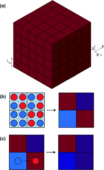
Recently, we described a scalable approach for robustly creating three-dimensional structures in the near-surface region of semiconductor substrates that may be useful as quantum-confined structures.26 Briefly, an indenter array fabricated by etching a silicon wafer is pressed against a SiGe wafer at elevated temperature, which creates a laterally patterned stress field in the near-surface region of the wafer. The stress field creates a thermodynamic driving force for compositional redistribution of the Si and Ge atoms, whereby the larger Ge atoms tend to move away from the areas of compressive stress; see Fig. 1. Following removal of the indenter array, the SiGe wafer was found to exhibit an array of pure Si “dots” located at the regions where the indenter tips were placed.
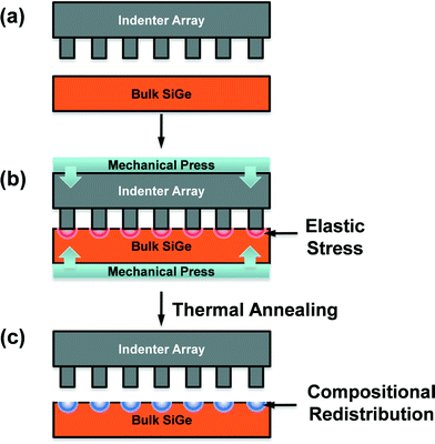 |
| | Fig. 1 A nanopillar template is applied to a SiGe wafer (a, b). During annealing, larger Ge atoms preferentially diffuse away from areas of compression, creating patches of enhanced Si content (c). Adapted from ref. 26. | |
This proof-of-concept study demonstrates that stress-mediated compositional patterning is a potentially attractive (i.e., simple, scalable and robust) route to creating addressable arrays of QCSs. However, employing this approach in practice to create useful QCS configurations (e.g., with sufficiently abrupt transitions between regions of strongly differing compositions—and therefore electronic bandgaps) will require an extensive assessment of the processing parameter space, which is both heterogeneous and high-dimensional. For example, the final compositional distribution is dependent on the indenter tip shape and size, the indenter array spacing and pattern, the annealing temperature–time history, as well as the initial substrate composition and thickness. Moreover, processing constraints require that annealing temperatures and indentation stresses be kept low enough to avoid the formation of plastic defects such as dislocations and stacking faults. Finding optimal designs for the compositional patterning approach will therefore require a large number of trials, and although a particular indenter array should be reusable, modifications of the array geometry will require a new one to be fabricated each time. Moreover, the characterization required to assess the outcome of each experiment is both time consuming and costly.26
For all of the above reasons, a quantitatively predictive atomistic simulation of the stress-mediated compositional patterning process is highly desirable; this is the subject of the present paper. Although additional models that predict the electronic band structure for the resulting compositional configurations would ultimately be required for ‘closing the design and optimization loop’, such modeling is outside the scope of the present work. The compositional evolution model is based on a coarse-grained lattice kinetic Monte Carlo simulation, in which the semiconductor domain is subdivided into a rigid lattice of cubic sub-volumes of a fixed size. Atomic exchanges between neighboring Si and Ge atoms are used to evolve the system configuration in time; the rates for these events are derived based on local values of the elastic stress, composition, and temperature. The coarse-graining enables the consideration of length and timescales that correspond directly to experimental conditions with reasonable computational expense. Next, key model elements, physical assumptions, and parameter values are introduced. The model is then used to assess how various parameters impact the compositional redistribution upon the action of indentation; in some cases, these predictions are compared to experimental observations. Finally, sensitivity analysis is presented for some of the important parameters.
Model
Point defect-mediated diffusion
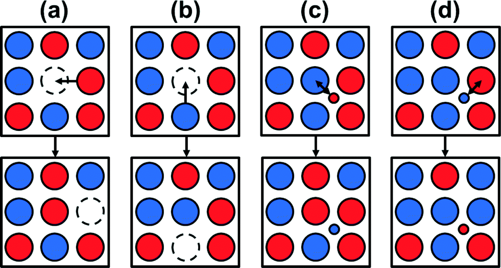
Diffusion of Si and Ge atoms in SiGe is mediated by native point defects (vacancies [V] and interstitials [I]) in one or more charge states; examples of point defect mediated diffusive processes are shown in Fig. 2 in which various point defects exchange positions with a neighboring lattice atom. Consequently, atomic diffusion in SiGe is intimately coupled to point defect diffusivities and concentrations, both of which are strong functions of temperature, composition, and lattice strain. Large numbers of the individual processes shown in Fig. 2 eventually lead to Si–Ge intermixing, or interdiffusion, which may be conceptualized as exchanges between neighboring lattice atoms. Note that direct simulation of interdiffusion with, say, molecular dynamics is infeasible for meaningful length and timescales because of the very low point defect equilibrium concentrations found in Si, Ge, and SiGe (below 1 × 10⁻⁶ atomic fraction at ∼1000 °C (ref. 27)). Consequently, some type of coarse-grained representation must be employed, as described in the following sections.
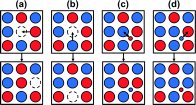 |
| | Fig. 2 Schematic of defect mediated atomic diffusion. Red atoms represent Si and blue atoms represent Ge: (a) vacancy-enabled Si motion, (b) vacancy-enabled Ge motion, (c) Si interstitial ‘kicks out’ a Ge atom creating a Ge interstitial, and (d) a Ge interstitial kicks out a Si atom creating a Si interstitial. | |
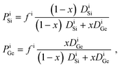
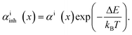
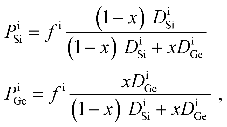
In a Si1−xGex bulk alloy, the probability of a particular mobile point defect species, i = I or V, moving a Si or Ge atom, respectively, is given by27
| |  | (1) |
where
DiSi(
x) and
DiGe(
x) are the (compositionally dependent) self-diffusivities of Si and Ge due to defect species i, and
fi is the correlation factor for atomistic motion caused by hops of defect species i (taken here to be 0.5 and 0.7 for the vacancies and interstitials, respectively
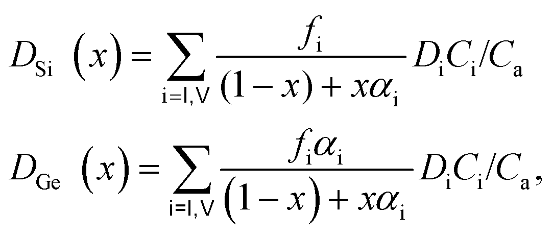
27). For a given point defect species, the self-diffusivities are related to the point defect transport capacity,
DiCi, according to
| | 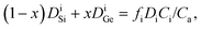 | (2) |
where
Ci is the concentration of point defect species i and
Ca is the total atomic site density (∼5 × 10
22 atoms per cm
3). Note that for each point defect species, the self-diffusivities and transport capacities include contributions summed over all the relevant charge states. Defining the ratio of Ge to Si self-diffusivity due to each point defect species,
i.e.,
DiGe(
x)/
DiSi(
x) ≡
αi(
x), and summing over both species then gives
27| | 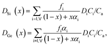 | (3) |
where
DSi (
x) and
DGe (
x) are the total Si and Ge self-diffusivities in a Si
1−xGe
x alloy. The point defect transport capacities and Ge-to-Si self-diffusivity ratios,
αi(
x,
T) =
αi0 (
x) exp (−
Eiα(
x)/
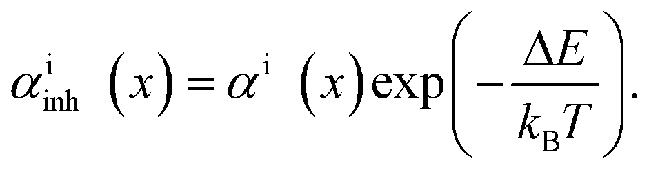
kBT), used in the present work are described in detail in Table 1 of
ref. 27. These parameters have been regressed to a large body of measurements obtained from dopant and isotope tracer diffusion experiments in stress-free and compositionally uniform Si, Ge, and Si
1−xGe
x alloys. Electronic structure calculations also were used to specify certain parameters that could not be extracted from experiment. These parameters are used here with no adjustment. Note that the regression procedure described in
ref. 27 ensures that the self-diffusivities and point defect transport capacities employed in the present LKMC simulations implicitly account for the effects of a variety of atomistic details including local atomic strains, electronic structure,
etc. In other words, while these details are not explicitly relevant in the present application, their impacts on point defect energies and mobilities are included to the extent that the model predicts the correct self-diffusivities and transport capacities as a function of composition and temperature.
Table 1 Elastic constants for Si, Ge and Si0.8Ge0.2 (ref. 47)
| Material |
C
11 (GPa) |
C
12 (GPa) |
C
44 (GPa) |
Young's modulus (GPa) |
Poisson's ratio |
| Si |
165.7 |
63.9 |
79.6 |
130.1 |
0.278 |
| Ge |
129.2 |
47.9 |
67.0 |
103.3 |
0.270 |
| Si0.8Ge0.2 |
158.4 |
60.7 |
77.0 |
124.8 |
0.277 |
Atomic diffusion under stress
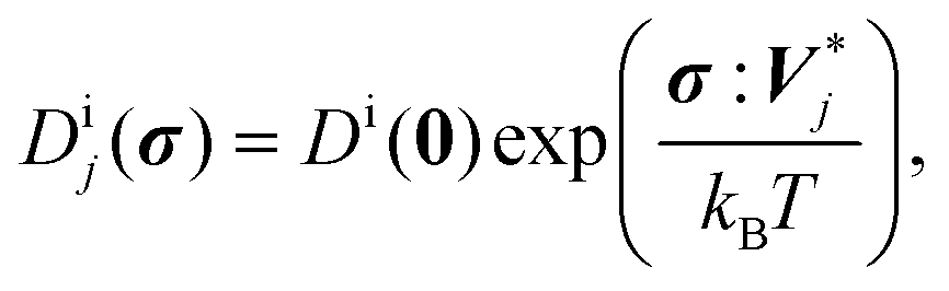
A theoretical framework for quantifying the impact of lattice stress on atomic diffusion has been described by Aziz,28 in which a stress field σ modifies the diffusivity of point defect species i according to| | 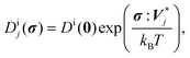 | (4) |
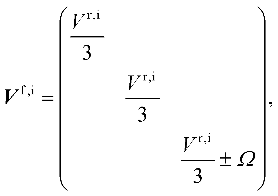
where V*,ij = Vf,i + Vm,ij is the activation volume tensor for hops along direction j, with Vf and Vmj being the formation and migration volume tensor contributions, respectively. For the (001)-oriented films we consider here, and assuming that the free surface is the only source of point defects, the formation volume tensor is given by27,28| | 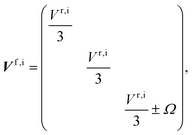 | (5) |
where Ω is the atomic volume that corresponds to the addition(subtraction) of an atom at the (001) surface to create a vacancy(self-interstitial) in the bulk. The relaxation volume, Vr,i, represents the additional volume change due to lattice relaxation following point defect generation. Off-diagonal components of the formation volume tensor are zero due to crystal symmetry.29 The migration volume tensor describes the additional volume change associated with point defect migration. In the (100) direction, the migration volume is given by| | 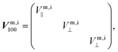 | (6) |
where Vm,i∥ and Vm,i⊥ represent changes parallel and perpendicular, respectively, to the direction of hopping motion. Similar expressions apply for migration along the other directions. The following parameter values for the activation volumes, which are used as base case values in the present study:27| | 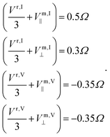 | (7) |
It should be noted that, generally, values for the various components of the activation volume tensor are not well established in the literature;30–36 sensitivity of the model predictions to these parameters is discussed briefly in the Results and discussion section. Finally, stress may also alter the band structure of the material, further modifying the diffusivities of point defects. However, these modifications were found to be relatively minor compared to the primary impact of stress27 and are neglected in this work.
Lattice kinetic Monte Carlo (LKMC) simulation
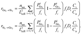
A coarse-grained LKMC37–39 simulation was developed in which a rigid, rectangular domain is subdivided into a lattice of cubic cells, each measuring Lcell in length and containing ntot (Si or Ge) atoms as shown in Fig. 3(a). Periodic boundary conditions are applied in the lateral directions (x and y) while no-flux boundary conditions are applied in the directions normal to the substrate surface (z). The microscopic distribution of the atoms in each cell is known to correspond to an ideal solid solution for most temperatures of interest, i.e., for a given composition, the Si and Ge atoms are mixed randomly.40 In other words, the mixing enthalpy of a mixture of Si and Ge atoms is zero, and the energetics associated with atomic exchanges do not vary with changes in microscopic configuration at a fixed overall composition. Consequently, only the overall composition in each cell is required to specify the state of the coarse-grained system; see Fig. 3(b).
 |
| | Fig. 3 (a) Schematic of an LKMC domain composed of cubic cells measuring Lcell in length and containing ntot Si and/or Ge atoms. (b) Schematic of coarse-graining atomic configurations in cells. Red atoms represent Si and blue atoms represent Ge. (c) Schematic of LKMC switch move. In the depicted exchange, a Ge atom is moving from the lower left to the lower right and a Si atom is moving from the lower right to the lower left. | |
Point defects within each cell are treated implicitly, and here are assumed to be always present in their equilibrium concentrations for given local composition, stress, and temperature. The assumption of quasi-equilibrium point defect distributions may be validated by considering that point defect equilibration proceeds via interaction with the nearby film surface that acts as a sink and source for point defects. For distances on the order of 10 microns, point defect diffusion timescales are of order 100 milliseconds, which, as will be demonstrated later in the discussion of the model predictions, is much faster than the timescales associated with compositional redistribution throughout the film. Of course, highly non-equilibrium processing, such as ion-implantation, would require accounting of non-equilibrium point defect distributions;27 such situations are not considered here.
The LKMC configuration state is evolved by a sequence of single Si–Ge ‘switch’ moves across two adjacent cells; see Fig. 3(c). We employ the ‘Next Reaction’ algorithm,41 along with a skip list42 to minimize event sorting cost. The compositions in the two participating cells are updated after every move. The rates at which the Si and Ge atoms are exchanged between two adjacent cells, ‘1’ and ‘2’, may be derived on the basis of the probabilities given in eqn (1), i.e.,
| |  | (8) |
The rate expressions in
eqn (8) describe an exchange of a Ge atom in cell ‘1’ with a Si atom in cell ‘2’ (top) or a Si atom in cell ‘1’ with a Ge in cell ‘2’ (bottom). The prefactors account for the total number of atoms in each cell,
ntot, and the distance over which the exchange is made,
Lcell. Point defect diffusivities and concentrations are calculated based on the average composition and stress of the two cells participating in the exchange.
As formulated, the rate expressions in eqn (8) do not automatically account for energy changes associated with Si–Ge exchange across cells with differing compositions and stresses; this information is required to ensure that the simulation predicts the correct equilibrium state. Following ref. 27, energy changes are accounted for by modifying the self-diffusivity ratios, αi (x, T), for each defect species to include the energy difference between moving a Ge atom and moving a Si atom, i.e.,
| |  | (9) |
For atomic motion across two adjacent cells, this energy difference can be shown to be equal to the energy difference resulting from an atomic switch across the two cells,
i.e.,
| |  | (10) |
where the subscripts i and j each refer to Si or Ge.
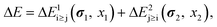
The energy change associated with an atomic switch across two cells was parametrized in terms of the cell stress state and cell composition. The stress state was defined in terms of the diagonal elements of the stress tensor, i.e., shear was assumed to be of secondary importance. For each instance, a periodic cubic cell containing 64 randomly distributed Si and Ge atoms arranged in a perfect diamond lattice configuration was first relaxed at a specified stress state with the conjugate gradient routine in LAMMPS43 based on the Tersoff potential.44–46 The identity of one randomly selected atom was then switched, the cell re-relaxed at constant volume, and the energy change recorded. It should be emphasized here that the ideal nature of the SiGe solid solution greatly simplifies these calculations because the switch energies do not depend on the microscopic configurations of the cell; this assumption was confirmed by repeating calculations for different microscopic realizations at a given overall composition for a few example cases. Energy changes corresponding to Si → Ge identity switches are shown in Fig. 4 as a function of stress and composition.
 |
| | Fig. 4 Energy change for a Si → Ge identity flip in a 64-atom cubic SixGe1−x cell at different combinations of stress state and composition. (a) Uniaxial stress, (b) biaxial stress, and (c) hydrostatic stress. Ge → Si identity flips lead to equal and opposite energy changes. | |
Results and discussion
The coarse-grained lattice kinetic Monte Carlo (LKMC) simulation framework described in the Model section was used to study Si and Ge interdiffusion in an initially homogeneously distributed Si0.8Ge0.2 film under the action of different nanoindenter-induced stress fields. Initial microscopic compositional fluctuations were imposed by randomly assigning identities to each (implicit) atom in every cell according to the desired overall composition. In all cases, stress fields in the SiGe film (and indenter) were computed by solving a linear elastic contact problem with the finite element method (FEM). Stress was generated by applying a specified body force on the indenter, pushing it into the SiGe film. For an infinitely-long cylindrical (‘wire’) contact, a two-dimensional, a plane strain elasticity model was employed. Here, periodic boundary conditions were applied in the x-direction, the bottom z-boundary was fixed, and the top z-boundary was traction-free except in the contact region. A two-dimensional axisymmetric model was used for spherical indenters. Traction-free boundary conditions were applied at the radial edge of the domain; the z-boundary conditions are the same as those for the wire indenter case.
LKMC simulations of cylindrical wire indentation were performed using two-dimensional domains that are one coarse cell thick along the wire axis (the y-direction). In the spherical indenter LKMC simulations, the axisymmetric stress field, defined in cylindrical coordinates (r, θ, z), was mapped onto a three-dimensional Cartesian LKMC domain. Although it is also possible to perform axisymmetric, effectively two-dimensional LKMC simulations in the spherical indenter case, such simulations require non-uniformly distributed LKMC coarse cells in order to ensure that the total number of atoms in each cell is constant.
Several assumptions and approximations were made in the calculation of stress fields. In the majority of the reported simulation results, we assumed that Si and Ge are elastically isotropic, which, as shown by the experimentally measured cubic elastic coefficients in Table 1,47 is not quite the case. As discussed below, this assumption does not strongly impact the LKMC results across a wide range of applied stress, while greatly simplifying the elastic stress computations. Isotropic elastic constants, namely the Young's modulus and Poisson's ratio, were computed along the <100> directions for both Si and Ge (Table 1). The properties for Si0.8Ge0.2 were obtained by linear interpolation of the elastic coefficients between the Si and Ge values, and then computing the corresponding Young's modulus and Poisson's ratio. We also assumed that the elastic properties of Si0.8Ge0.2 are applicable to the entire domain at all times during thermal annealing. Of course, in actuality, local compositional changes during annealing would lead to changes in the local mechanical properties and therefore the applied stress field; however, we show later that this simplifying assumption has little practical impact on the model predictions. Finally, all elastic coefficients are assumed to be independent of temperature.
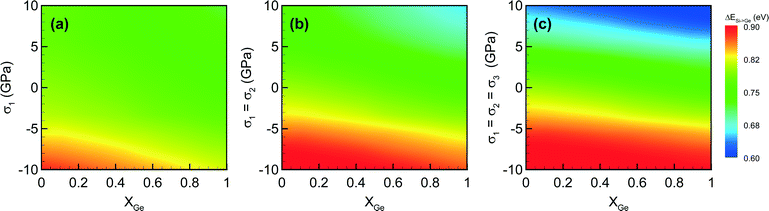
Shown in Fig. 5(a) is an example plane strain stress field (σzz) generated by an infinite cylindrical wire indenter with a diameter of 80 nm, assuming isotropic mechanical properties of Si0.8Ge0.2. Note that the stress field is mapped onto the undeformed (LKMC) domain. The Si0.8Ge0.2 film dimensions, which were also used for all LKMC wire indenter simulations, are 210.3 nm in the x-direction (corresponding to 384 Si0.8Ge0.2 unit cells with lattice parameter 0.5476681 nm (ref. 29)) and 157.7 nm in the z-direction (288 unit cells). In Fig. 5(b), the maximum contact pressure (−σzz at the center of the contact zone48) is shown as a function of indenter force per unit length of the cylindrical indenter for three calculations. The anisotropic case is shown by the blue line, the corresponding isotropic case is shown in green, and the result of a Hertzian contact analysis is shown by the black dashed line. For maximum contact pressures less than about 10 GPa, all three cases are in excellent quantitative agreement. Slightly larger deviations are visible as the maximum contact pressure is increased to 20 GPa, but these are generally less than about 5%, justifying the use of the isotropic elasticity assumption.
 |
| | Fig. 5 (a) Stress (σzz) in the xz-plane generated by an infinite (in y) cylindrical wire indenter of diameter 80 nm, corresponding to a maximum contact pressure of 15 GPa, mapped onto the undeformed domain. Results from plane strain calculation assuming isotropic elasticity. (b) Indenter force versus maximum contact pressure for an 80 nm-diameter, infinitely long, cylindrical indenter against Si0.8Ge0.2. Blue line – anisotropic elasticity, green line – isotropic elasticity, black dashed line – Hertz contact model. | |
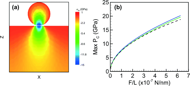
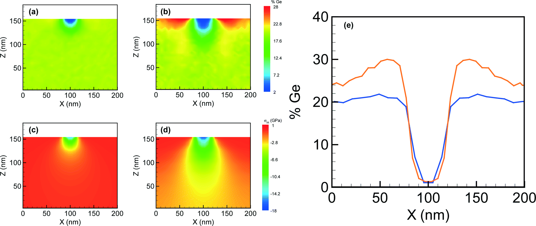
As described in the Introduction, stress-directed compositional patterning has been demonstrated experimentally and reported in a prior publication.26 In this demonstration, an indenter array was created by etching a Si wafer to produce an array of rods with approximately spherical tips; see Fig. 6(e). The indenter array consisted of a square lattice of 80 nm-diameter rods, spaced at a 200 nm pitch. The indenter array was then pressed against a Si0.8Ge0.2 wafer using a mechanical press and subjected to thermal annealing at a fixed temperature for three hours. Several annealing temperatures and indenter forces were considered in the experiments. Following annealing the Si0.8Ge0.2 wafers were analyzed using a combination of cross-sectional tunneling electron microscopy (XTEM) and energy dispersive spectroscopy (EDS) to assess the compositional distribution in the vicinity of the indenter contact regions. We note here that the XTEM and EDS analysis was only performed for cases in which the maximum contact pressure, as estimated by the Hertzian analysis, was above ∼35 GPa, which is generally higher than the situations considered here computationally. In fact, such high indenter forces are generally undesirable because of the risk of plastic deformation in the film, and because of damage to the indenter array as well as the film surface. Nonetheless, these cases were used for the imaging and compositional analysis because the surface damage served as a ‘marker’ for the indenter locations.
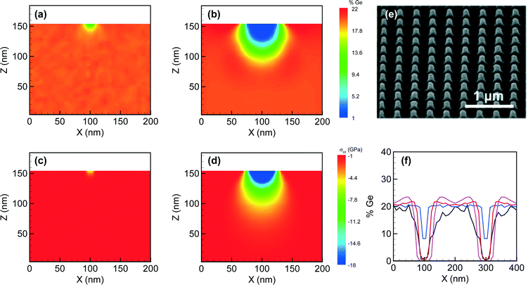 |
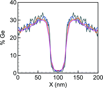
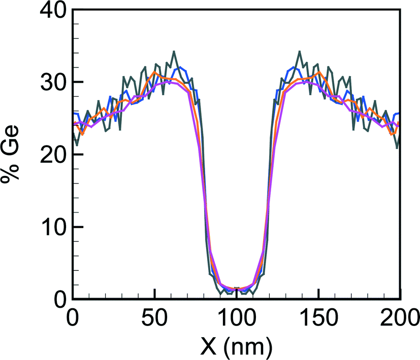
| | Fig. 6 Simulated Ge concentration profiles (a, b) in an initially uniform Si0.8Ge0.2 film following 3 hours of thermal annealing at 1000 °C under stresses (c, d) induced by contact with an 80 nm-diameter spherical indenter with a maximum contact pressure of 9 GPa (a, c) and 35 GPa (b, d). Note that (a)–(d) show the xz-plane of the three-dimensional simulation domain taken at the center of contact in y; this convention is used throughout the paper. (e) Scanning electron microscopy (SEM) image of the Si nanopillar indenter array used in the experiments reported in ref. 26. (f) Near-surface (see text) Ge concentration as a function of the x-position. Black line – experimental EDS measurement with a maximum contact pressure of ∼35 GPa (based on Hertz contact model), blue line – LKMC with a maximum contact pressure of 9 GPa, red line – LKMC simulation with a maximum contact pressure of 21 GPa, purple line – LKMC with a maximum contact pressure of 35 GPa. All LKMC simulations performed with coarse cell size Lcell = 6.56 nm. Note that the simulation profiles in (f) represent two copies of the actual simulation domain. | |
Shown in Fig. 6(a and b) are the Ge concentration profiles in an initially uniform Si0.8Ge0.2 domain predicted by LKMC simulation following three hours of thermal annealing at 1000 °C under the action of a spherical 80 nm-diameter indenter. For all spherical indenter simulations, we employed an LKMC domain with dimensions 210.3 nm (384 unit cells) × 210.3 nm (384 unit cells) × 157.7 nm (288 unit cells) in x, y, and z, respectively. Shown in snapshot (a) is the composition for the case where the maximum contact pressure is 9 GPa, while (b) corresponds to a maximum contact pressure of 35 GPa. Shown in panels (c and d) are the corresponding applied stress fields. The computed Ge concentration profiles along the x-direction are shown in Fig. 6(f) for the top layer of LKMC cells for the two indenter cases, as well as an intermediate case where the maximum contact pressure was 21 GPa. Note that the profiles represent two periodic images of the actual LKMC domain placed side-by-side in the x-direction. Also shown in Fig. 6(f) are the results of EDS analysis at an estimated maximum contact pressure of 35 GPa.26
Both the 21 GPa and 35 GPa simulations show essentially complete Ge depletion below the indenter, in agreement with the experimental profiles. However, discrepancies exist in the shape of the depletion zone. While the 21 GPa simulation result appears to align well with the experimental profile in the center of the depletion zone, the 35 GPa case shows a wider zone of complete depletion. On the other hand, neither case shows the broad partial depletion zone exhibited in the experimental profile. There are several factors that may contribute to the discrepancy. First, the activation volume parameters discussed earlier in the paper, which describe the dependence of diffusion rates on stress, are somewhat uncertain. Although, in principle, these parameters were validated in ref. 27 by comparison to interdiffusion experiments, the stresses considered here are far larger and uncertainty in these parameters could have more significant impact. Computational estimates of these parameters along with an analysis of the sensitivity of the model to them, will be considered in future work. Second, our assumption of a spherical indenter tip may not be accurate; it is difficult to determine the indenter tip shape from the image in Fig. 6(e) and further analysis would be required to obtain a better representation. Next, it is possible that the high indenter forces lead to plastic deformation of the indenters, changing both the applied stress and the effective tip shape during the annealing process. Although no plastic deformation was observed by XTEM in the Si0.8Ge0.2 wafer, the large indenter force led to fusing between the indenter and Si0.8Ge0.2 substrate surface, which may be associated with some non-elastic deformation of the indenter. Again, additional analysis of the indenter array following the annealing process would be required to rule out this possibility. Lastly, we note that the experimental measurements of the composition are themselves subject to some uncertainty, which we estimate here to be less than about 1–2% in the reported composition, based on the EDS beam intensity calibration procedure reported in ref. 26. Taken together, these uncertainties may suggest that a quantitatively perfect prediction of the exact shape of the depletion zone below each indenter may be an ill-posed goal, and that ‘coarser’ measures, such as the extent of depletion, and the overall collective pattern created by arrays of indenters, are better ones to target with simulations. Further experiments and corresponding simulations will be required to fully assess this issue.
A more subtle discrepancy between the simulation and experimental compositional profiles in Fig. 6(f) may be observed in the fluctuation amplitude, which is notably higher in the experimental case. The EDS technique used in ref. 26 produces compositions that are averages over cubic domains at the surface that are estimated to be about 3 × 3 × 3 nm3 in size. On the other hand, the LKMC cubic cells used to generate the data in Fig. 6 were chosen to be 6.56 nm on a side (corresponding to 12 unit cells of Si0.8Ge0.2 with lattice parameter 0.547681 nm), representing an approximately 10-fold increase in the number of atoms per averaging sub-volume. Our choice of Lcell = 6.56 nm, which is used for all simulations in this paper, was largely predicated on computational cost; LKMC simulations with double the resolution in each dimension, i.e., Lcell = 3.28 nm, take about 8 times longer to perform than those at the Lcell = 6.56 nm resolution, which was rather prohibitive for the fully three-dimensional LKMC simulations used in the spherical indenter cases. However, as shown in Fig. 7 for a set of reference two-dimensional wire indenter simulations with different coarse cell sizes, the impact of cell size is largely restricted to the magnitude of compositional fluctuations and does not materially alter the nature of the compositional profile.
 |
| | Fig. 7 Ge concentration profiles in the top layer of coarse cells of a Si0.8Ge0.2 substrate subjected to a 80 nm-diameter cylindrical wire indenter following 3 hours of annealing at 1000 °C. The maximum contact pressure was 18 GPa. Individual profiles obtained with different LKMC coarse cell sizes: Gray – Lcell = 2.19 nm (512 atoms per cell), blue – Lcell = 3.28 nm (1728 atoms per cell), orange – Lcell = 4.37 nm (4096 atoms per cell), pink – Lcell = 6.56 nm (13![[thin space (1/6-em)]](https://www.rsc.org/images/entities/char_2009.gif) 824 atoms per cell). Note that all wire indenter simulations are based on two-dimensional LKMC domains that are a single cell thick in the y-direction. 824 atoms per cell). Note that all wire indenter simulations are based on two-dimensional LKMC domains that are a single cell thick in the y-direction. | |
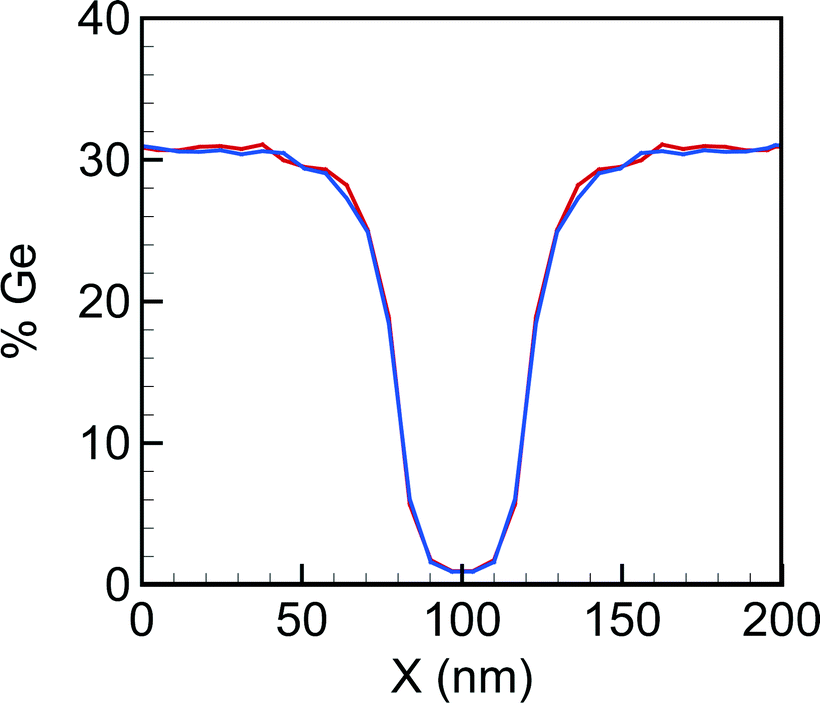
We also used the wire indenter case to test an important assumption that was introduced earlier, namely that the stress field does not need to be dynamically updated as the compositional redistribution takes place. Shown in Fig. 8 are the steady-state Ge concentrations (annealing time much longer than 3 hours) in the top layer of cells under the same conditions as those used to generate Fig. 7. The black line shows the solution using the elastic constants of the initial homogeneous Si0.8Ge0.2 material. The blue line shows the profile that results when the steady-state compositional field is subsequently used to update the elastic constants (which now become spatially varying), and the simulation continued until it attains a new steady-state. The fact that these profiles are essentially identical confirms that, at least for Si and Ge, the differences in the elastic constants do not play qualitatively important roles in the compositional redistribution.
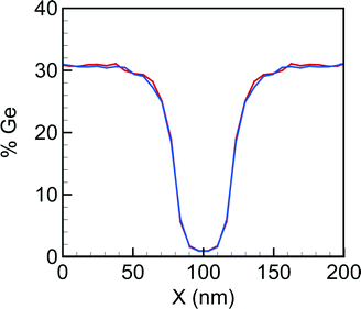 |
| | Fig. 8 Steady-state Ge concentration profiles in the top layer of LKMC cells of an initially uniform Si0.8Ge0.2 film subjected to an 80 nm-diameter wire indenter (maximum contact pressure of 18 GPa) and annealed at 1000 °C. Red line – elastic constants corresponding to initial (uniform) composition, blue line – with elastic constants corresponding to a spatially-varying steady-state compositional profile. | |
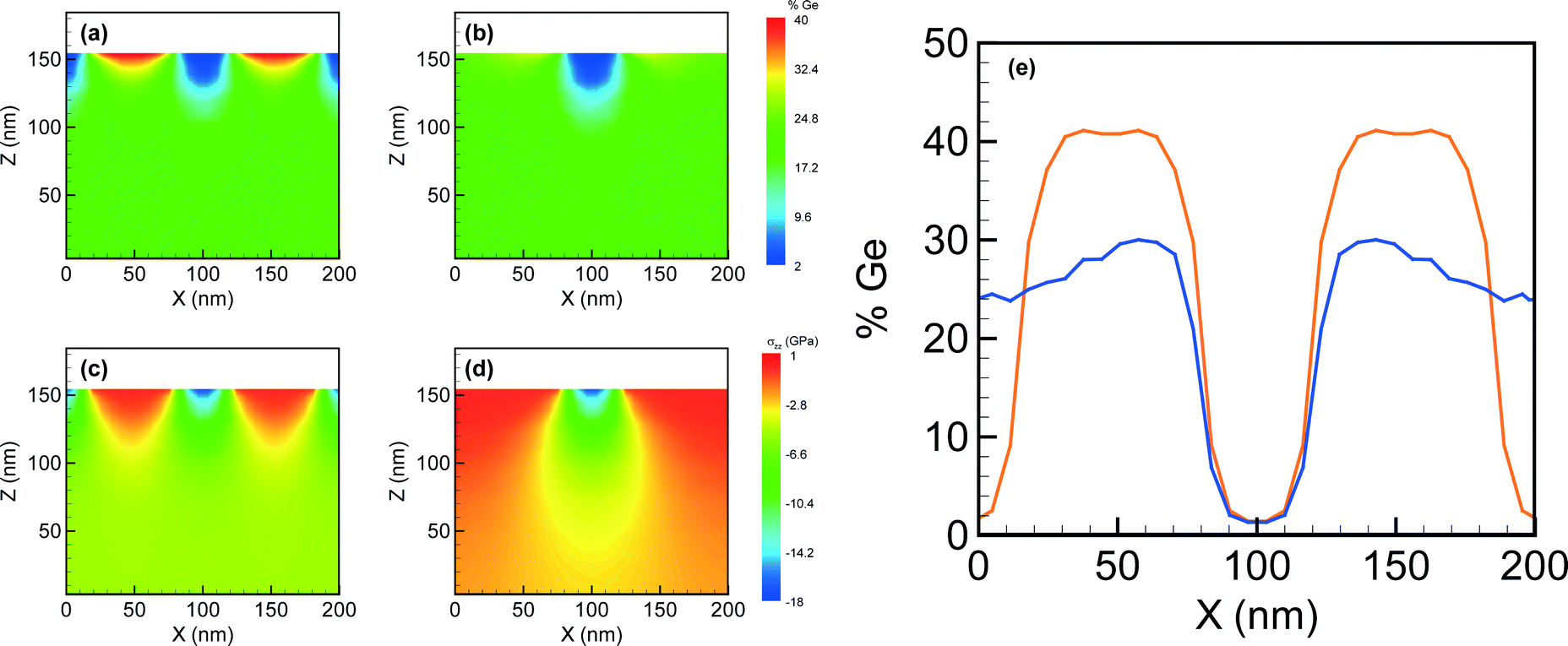
Next, the dependence of the Ge depletion effect on the type of indenter was investigated. As shown in Fig. 9, wire indenters lead to qualitatively different stress fields compared to those produced by the spherical indenters. Most notably, the near-surface regions just outside the wire contact zone are tensilely stressed and therefore tend to attract Ge atoms resulting in enhanced Ge concentrations above the background 20% value. Consequently, the Ge profiles resulting from wire indentation show a stronger Ge concentration difference at the edge of the depletion zone, which may be useful in the context of QCS design where large concentration changes across small distances are required for confinement and isolation. Although not shown here, upon further annealing the region of enhanced Ge concentration gradually continues to broaden and eventually extends across nearly the entire near-surface region.
 |
| | Fig. 9 Simulated Ge concentration profiles (a, b) in an initially uniform Si0.8Ge0.2 film following 3 hours of thermal annealing at 1000 °C under stresses (c, d) induced by contact with (a) an 80 nm-diameter spherical indenter, and (b) an 80 nm-diameter wire indenter, both with a maximum contact pressure of 18 GPa. (e) Compositional profiles in the top layer of cells; orange line – wire indenter, blue line – spherical indenter. As noted earlier, the spherical indenter LKMC simulation results represent an xz-slice taken from a three-dimensional domain, while the wire indenter simulations are two-dimensional. | |
In fact, any practical approach for QCS engineering in the present context will require the capability of enhancing Ge in localized regions. Generally speaking, ideal quantum confinement structures are composed of sharply delineated regions of a lower bandgap material, isolated by a surrounding material with a higher electronic bandgap.49 Given that the bandgap of SiGe decreases with Ge composition,50 a QCS-relevant configuration requires a high Ge concentration region surrounded by a lower Ge concentration. The stress patterning approach described here generally tends to push the Ge atoms away because the applied stress is mostly compressive in nature. Building on the results in Fig. 9, we simulated the Ge distribution in a system where two wire indenters were placed 105 nm apart, rather than the 210 nm pitch used in the previous simulations. As shown in Fig. 10, this configuration (orange line) leads to well-defined regions of Ge enhancement (over 40%) separated by almost completely Ge-depleted regions by very high compositional gradients. In contrast, the 210 nm pitch configuration (blue line) only produces a peak Ge concentration of 30%, and which is non-uniform across the Ge-enhanced region. These results provide preliminary evidence for the ability of the stress-mediated patterning approach to produce technologically relevant compositional configurations. Systematic optimization of indenter configuration is tantamount to solving an inverse problem in which the indenter geometry, along with other processing parameters, is found for a given desired (and feasible) compositional configuration; this will be the subject of future work.
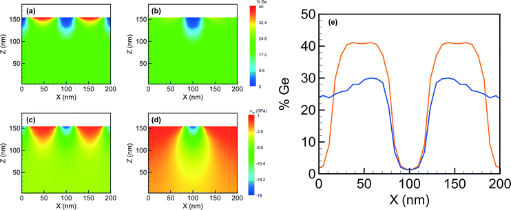 |
| | Fig. 10 Ge concentration profiles (a, b) in an initially uniform Si0.8Ge0.2 film following 3 hours of thermal annealing at 1000 °C under stresses (c, d) induced by contact with an 80 nm-diameter wire indenter (maximum contact pressure of 18 GPa) with inter-wire spacing of (a, c) 105 nm and (b, d) 210 nm. (e) Compositional profiles in the top layer of cells; orange line – 105 nm pitch, blue line – 210 nm pitch. | |
Finally, we address the dynamics of stress-mediated Ge redistribution. The temporal evolution of the Ge profile during thermal annealing at 1000 °C under applied stress is shown in Fig. 11 for the case of an 80 nm-diameter spherical indenter exerting a 21 GPa maximum contact pressure. As shown by the two-dimensional compositional profiles (a–d) and the near-surface compositional scans (e), three hours is sufficient for the Ge compositional distribution to reach steady state, at least in the region of strong Ge depletion. The impact of annealing temperature on the redistribution dynamics was analyzed by considering the Ge evolution due to the application on an 80 nm-diameter wire indenter (maximum contact pressure of 18 GPa). As expected, the diffusion-mediated process follows Arrhenius behavior in which the time to reach the patterned configuration shown in Fig. 12(a), was found to obey an Arrhenius relationship of the form  . The best fit is shown in Fig. 12(b): a = 1.5 × 10⁻¹⁴ minutes and b = 4.7 × 10⁴ K. In practice, increased redistribution dynamics with higher temperatures must be balanced against material softening and a higher chance for plastic defect formation. We also note that point defect diffusivity is also strongly influenced by stress as discussed in the Model section, and the activation volume parameters reported in eqn (7) also are expected to have substantial effects on the patterning timescale. A limited sensitivity analysis with respect to these parameters was performed in which all 4 parameters were scaled by a single constant ranging from 0.75–2.0. The results (not shown) indicate that while the final Ge distribution is unaffected by the activation volume scaling, the timescale for patterning is, unsurprisingly, quite sensitive to these parameters. The large uncertainty in the overall dynamics of the compositional patterning process associated with these parameters will be addressed in a future publication.
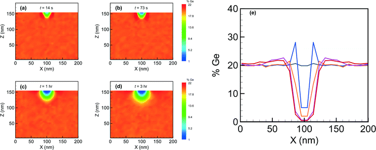 |
| | Fig. 11 (a)–(d) Sequence of snapshots of Ge concentration fields in a SiGe film during annealing at 1000 °C under a spherical indenter of diameter 80 nm and a maximum contact pressure of 21 GPa, (e) Ge concentration profile in the top layer of LKMC cells after 0 s (grey), 14 s (blue), 74 s (orange), 1 hour (pink) and 3 hours (red). | |
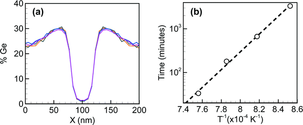 |
| | Fig. 12 (a) Ge concentration in the top layer of LKMC cells in an initially uniform Si0.8Ge0.2 film following annealing for variable times under the action of a 80 nm-diameter wire indenter (maximum contact pressure 18 GPa). Annealing times are 30 min at 1050 °C (pink), 180 min at 1000 °C (blue), 700 min at 950 °C, and 3300 min at 900 °C. (b) Arrhenius plot of the annealing time to reach set patterning extent versus inverse temperature; circles are simulation data, dashed line is the Arrhenius fit. | |
Conclusions
The ability to compositionally pattern large-area thin films composed of solid-solution alloys (e.g., SiGe) using elastic fields generated by ordered arrays of nano-indenters presents an exciting opportunity to engineer laterally organized, three-dimensionally quantum-confined structures. The essential idea behind this approach is appealingly simple—the larger atomic species in the alloy will be driven away by diffusion from regions of compression immediately below the indenters, creating lateral, as well as vertical, compositional gradients. Although ‘proof-of-principle’ experimental demonstrations have been successful, it is immediately obvious that optimization of stress-driven compositional patterning requires the simultaneous consideration of numerous process parameters and constraints. Example parameters include indenter shape, pitch and array geometry, annealing temperature–time history, and initial alloy composition, to name a few. Constraints include the formation of plastic defects such as dislocations if the stresses created by the indenters are too high. Such defects may pose irreversible sinks for point defects, hindering the patterning process. Given the challenges associated with characterization of the structure and composition at the nanoscale in such materials, a predictive model for stress-driven compositional patterning is highly desirable for carrying out systematic studies.
The goals of this paper are two-fold. First, it was shown that such a model can indeed be constructed, even though interdiffusion in SiGe is surprisingly complex given the strong dependence of point defect diffusion (which is the primary transport mediator) on time- and space-varying temperature, composition and stress. Second, we used the model to investigate the impact of some of the process parameters on the resulting compositional patterns. Most importantly, we were able to demonstrate that it is possible to enhance, as well as deplete, the Ge concentrations. In its simplest interpretation, the stress-driven compositional patterning approach described here provides a ‘one-way’ control, in which the larger Ge atoms are driven away from localized regions of high compressive stress below each indenter, leaving behind locally Si-enriched regions embedded in the SiGe background. Unfortunately, such configurations are not useful as QCSs because quantum confinement requires that the smaller bandgap region (high Ge content) be embedded in a larger bandgap environment (low Ge content). However, using wire-like indenters that are closely spaced, we found that localized regions of tensile stress can be created in the near-surface region of the alloy substrate, which then attract Ge atoms and create well-defined regions in which the Ge content is above the background alloy composition. While these results are somewhat preliminary, they do suggest that optimization of the approach could lead to very useful compositional configurations—this will be the subject of future investigations.
Acknowledgements
We gratefully acknowledge support from the National Science Foundation (CMMI-1068970 and CMMI-1068841).
References
- G. W. Bryant, Phys. Rev. Lett., 1987, 59, 1140–1143 CrossRef CAS PubMed.
- Q. Sun, Y. A. Wang, L. S. Li, D. Y. Wang, T. Zhu, J. Xu, C. H. Yang and Y. F. Li, Nat. Photonics, 2007, 1, 717–722 CrossRef CAS.
- N. Kirstaedter, N. N. Ledentsov, M. Grundmann, D. Bimberg, V. M. Ustinov, S. S. Ruvimov, M. V. Maximov, P. S. Kop'ev, Z. I. Alferov and U. Richter, Electron. Lett., 1994, 30, 1416–1417 CrossRef CAS.
- Y. Narukawa, Y. Kawakami, M. Funato, S. Fujita, S. Fujita and S. Nakamura, Appl. Phys. Lett., 1997, 70, 981–983 CrossRef CAS.
- P. Zanardi and F. Rossi, Phys. Rev. Lett., 1998, 81, 4752–4755 CrossRef CAS.
- Y. S. Weinstein, C. S. Hellberg and J. Levy, Phys. Rev. A: At., Mol., Opt. Phys., 2005, 72, 020304 CrossRef.
- D. Loss and D. P. DiVincenzo, Phys. Rev. A: At., Mol., Opt. Phys., 1998, 57, 120–126 CrossRef CAS.
- R. Raussendorf and H. J. Briegel, Phys. Rev. Lett., 2001, 86, 5188–5191 CrossRef CAS PubMed.
- P. M. Petroff, A. Lorke and A. Imamoglu, Phys. Today, 2001, 54, 46–52 CrossRef CAS.
- A. K. Ekert, Phys. Rev. Lett., 1991, 67, 661–663 CrossRef PubMed.
- C. B. Murray, D. J. Norris and M. G. Bawendi, J. Am. Chem. Soc., 1993, 115, 8706–8715 CrossRef CAS.
- X. Peng, L. Manna, W. Yang, J. Wickham, E. Scher, A. Kadavanich and A. P. Alivisatos, Nature, 2000, 404, 59–61 CrossRef CAS PubMed.
- B. O. Dabbousi, J. Rodriguez-Viejo, F. V. Mikulec, J. R. Heine, H. Mattoussi, R. Ober, K. F. Jensen and M. G. Bawendi, J. Phys. Chem. B, 1997, 101, 9463–9475 CrossRef CAS.
- D. Bimberg, M. Grundmann, N. N. Ledentsov, S. S. Ruvimov, P. Werner, U. Richter, J. Heydenreich, V. M. Ustinov, P. S. Kop'ev and Z. I. Alferov, Thin Solid Films, 1995, 267, 32–36 CrossRef CAS.
- F. Heinrichsdorff, M.-H. Mao, N. Kirstaedter, A. Krost, D. Bimberg, A. O. Kosogov and P. Werner, Appl. Phys. Lett., 1997, 71, 22–24 CrossRef CAS.
- F. M. Ross, M. Kammler, M. C. Reuter and R. Hull, Philos. Mag., 2004, 84, 2687–2697 CrossRef CAS.
- F. M. Ross, R. M. Tromp and M. C. Reuter, Science, 1999, 286, 1931–1934 CrossRef CAS PubMed.
- O. G. Schmidt, N. Y. Jin-Phillipp, C. Lange, U. Denker, K. Eberl, R. Schreiner, H. Grabeldinger and H. Schweizer, Appl. Phys. Lett., 2000, 77, 4139–4141 CrossRef CAS.
- J. J. Zhang, M. Stoffel, A. Rastelli, O. G. Schmidt, V. Jovanovic, L. K. Nanver and G. Bauer, Appl. Phys. Lett., 2007, 91, 173115 CrossRef.
- J. M. Baribeau, X. Wu, N. L. Rowell and D. J. Lockwood, J. Phys.: Condens. Matter, 2006, 18, R139–R174 CrossRef CAS.
- J. H. Zhu, K. Brunner and G. Abstreiter, Appl. Phys. Lett., 1998, 73, 620–622 CrossRef CAS.
- T. Sekiguchi, S. Yoshida, Y. Shiren, K. M. Itoh, J. Myslivecek and B. Voigtlander, J. Appl. Phys., 2007, 101, 081702 CrossRef.
- B. Voigtlander and N. Theuerkauf, Surf. Sci., 2000, 461, L575–L580 CrossRef CAS.
- C. Teichert, C. Hofer, K. Lyutovich, M. Bauer and E. Kasper, Thin Solid Films, 2000, 380, 25–28 CrossRef CAS.
- P. Liu, C. Lu and Y. W. Zhang, Phys. Rev. B: Condens. Matter Mater. Phys., 2007, 76, 085336 CrossRef.
- S. Ghosh, D. Kaiser, J. Bonilla, T. Sinno and S. M. Han, Appl. Phys. Lett., 2015, 107, 072106 CrossRef.
- P. Castrillo, R. Pinacho, M. Jaraiz and J. E. Rubio, J. Appl. Phys., 2011, 109, 103502 CrossRef.
- M. J. Aziz, Appl. Phys. Lett., 1997, 70, 2810–2812 CrossRef CAS.
- M. J. Aziz, Y. C. Zhao, H. J. Gossmann, S. Mitha, S. P. Smith and D. Schiferl, Phys. Rev. B: Condens. Matter Mater. Phys., 2006, 73, 054101 CrossRef.
- C. L. Allred, X. Yuan, M. Z. Bazant and L. W. Hobbs, Phys. Rev. B: Condens. Matter Mater. Phys., 2004, 70, 134113 CrossRef.
- S. A. Centoni, B. Sadigh, G. H. Gilmer, T. J. Lenosky, T. D. de la Rubia and C. B. Musgrave, Phys. Rev. B: Condens. Matter Mater. Phys., 2005, 72, 195206 CrossRef.
- A. Antonelli and J. Bernholc, Phys. Rev. B: Condens. Matter Mater. Phys., 1989, 40, 10643–10646 CrossRef CAS.
- A. Antonelli, E. Kaxiras and D. J. Chadi, Phys. Rev. Lett., 1998, 81, 2088–2091 CrossRef CAS.
- K. Sueoka, E. Kamiyama, H. Kariyazaki and J. Vanhellemont, Phys. Status Solidi C, 2012, 9, 1947–1951 CrossRef CAS.
- M. J. Tang, L. Colombo, J. Zhu and T. D. de la Rubia, Phys. Rev. B: Condens. Matter Mater. Phys., 1997, 55, 14279–14289 CrossRef CAS.
- W. Windl, M. S. Daw, N. N. Carlson and M. Laudon, Mater. Res. Soc. Symp. Proc., 2001, 677, AA9.4.1–AA9.4.6 CrossRef.
- J. Dai, W. D. Seider and T. Sinno, Mol. Simul., 2006, 32, 305–314 CrossRef CAS.
- K. A. Fichthorn and W. H. Weinberg, J. Chem. Phys., 1991, 95, 1090–1096 CrossRef CAS.
- A. B. Bortz, M. H. Kalos and J. L. Lebowitz, J. Comput. Phys., 1975, 17, 10–18 CrossRef.
- F. Edelman, Y. Komem, P. Werner, J. Heydenreich, R. Butz and S. S. Iyer, J. Cryst. Growth, 1995, 157, 177–180 CrossRef CAS.
- M. A. Gibson and J. Bruck, J. Phys. Chem. A, 2000, 104, 1876–1889 CrossRef CAS.
- W. Pugh, Commun. ACM, 1990, 33, 668–676 CrossRef.
- S. Plimpton, J. Comput. Phys., 1995, 117, 1–19 CrossRef CAS.
- J. Tersoff, Phys. Rev. B: Condens. Matter Mater. Phys., 1988, 38, 9902–9905 CrossRef CAS.
- J. Tersoff, Phys. Rev. B: Condens. Matter Mater. Phys., 1989, 39, 5566–5568 CrossRef.
- J. Tersoff, Phys. Rev. B: Condens. Matter Mater. Phys., 1988, 37, 6991–7000 CrossRef.
- W. A. Brantley, J. Appl. Phys., 1973, 44, 534–535 CrossRef CAS.
-
K. L. Johnson, Contact Mechanics, Cambridge University Press, Cambridge, UK, 1985 Search PubMed.
- A. P. Alivisatos, Science, 1996, 271, 933–937 CAS.
- C. S. Wang and B. M. Klein, Phys. Rev. B: Condens. Matter Mater. Phys., 1981, 24, 3393–3416 CrossRef CAS.
|
| This journal is © The Royal Society of Chemistry 2016 |
Click here to see how this site uses Cookies. View our privacy policy here. 
 a,
Swapnadip
Ghosh
b,
Sang M.
Han
b and
Talid
Sinno
*a
a,
Swapnadip
Ghosh
b,
Sang M.
Han
b and
Talid
Sinno
*a


 . The best fit is shown in Fig. 12(b): a = 1.5 × 10⁻¹⁴ minutes and b = 4.7 × 10⁴ K. In practice, increased redistribution dynamics with higher temperatures must be balanced against material softening and a higher chance for plastic defect formation. We also note that point defect diffusivity is also strongly influenced by stress as discussed in the Model section, and the activation volume parameters reported in eqn (7) also are expected to have substantial effects on the patterning timescale. A limited sensitivity analysis with respect to these parameters was performed in which all 4 parameters were scaled by a single constant ranging from 0.75–2.0. The results (not shown) indicate that while the final Ge distribution is unaffected by the activation volume scaling, the timescale for patterning is, unsurprisingly, quite sensitive to these parameters. The large uncertainty in the overall dynamics of the compositional patterning process associated with these parameters will be addressed in a future publication.
