Temperature dependent behaviour of lead sulfide quantum dot solar cells and films†
Received
2nd June 2016
, Accepted 11th August 2016
First published on 11th August 2016
Abstract
Despite increasing greatly in power conversion efficiency in recent times, lead sulfide quantum dot (PbS QD) solar cells still suffer from a low open circuit voltage (VOC) and fill factor (FF). In this work, we explore the temperature dependent behavior of ∼9% efficient solar cells. In the temperature range of 290 to 230 K, we find increased VOC and FF values without significant degradation of the short circuit current, leading to up to 10.3% efficiency at 230 K. The change in VOC is driven by the decrease of the reverse saturation current which fits the PN-junction model. Using Schottky and single carrier devices, we measure the carrier mobility, diffusion lengths, and doping concentrations of PbS QD films with tetrabutylammonium iodide and ethane dithiol ligands as a function of temperature. Both mobility and diffusion length are found to decrease with decreasing temperature while device performance increases, indicating that the 260 nm thick active layer is fully depleted. Finally, we propose that further optimization of the doping concentrations could help achieve increased device performance at room temperature.
Broader context
The increasing need for clean, renewable, and cheap energy sources has driven the research of a new generation of low-cost and highly efficient solar cells. Lead sulfide colloidal quantum dots (PbS QDs) are promising candidates for solar cell applications due to their size tunable bandgap, broad absorption profile, and their compatibility with large-scale production techniques. Recent progress has led to efficiencies above 10%, but the performance is still limited by a low open circuit voltage (VOC) and fill factor (FF). In this report, we systematically measure the temperature dependent behaviour of the most important physical properties of state-of-the-art solar cells in order to determine the limiting factors of the VOC and FF. We then provide practical and quantitative guidelines for further efficiency enhancement.
|
1 Introduction
Lead sulfide quantum dots (PbS QDs) have been a topic of intense study for over a decade due to their excellent optoelectronic properties and their large versatility in such applications as infrared sensors,1–4 infrared photon sources,5 transistors,6–8 and solar cells.9–12 Their versatility stems mainly from the size dependent bandgap and the wide array of possible ligands and surface modifications which allow low cost device processing from solution and facile modification of the electronic properties. PbS QD solar cells in particular have seen a rapid rise in solar cell performance, from less than 1% in 2005 to 10.6% in 2015.1,11 This progress has been made possible by several factors. First, improvements in the synthesis of the QDs have increased the monodispersity and scalability of PbS QDs.13,14 Secondly, a vast body of research has been carried out to improve post-deposition passivation of QD films,15–18 which has been shown to reduce trap density and allows tuning of the band positions and Fermi levels.19 Finally, an improved understanding of energy level alignment and band bending has led to increasingly sophisticated device structures which facilitate the extraction of generated charges.12,20–22 To further improve solar cell efficiencies, the prevailing limitations must be understood. Presently, the open circuit voltage (VOC) in particular falls well short of its theoretical maximum and must be improved if PbS QD solar cells are to become a viable technology.23,24 Studying the temperature dependent properties of PbS films has been very successful at probing both the optical and electronic properties of thiol-capped QDs,25,26 but as yet no such study has been done for state-of-the-art solar cells. Moreover, no such study has been carried out for halide ligands which have become widespread in the QD field and which behave very differently to thiol ligands in many respects.27,28
In this work, we report the temperature dependent behavior of highly efficient solar cells comprising a layer of tetrabutylammonium iodide (TBAI) capped PbS and a layer of ethane dithiol (EDT) capped PbS. We observe a large increase in device performance at lower temperatures, mainly due to an increased VOC and fill factor (FF) with only a slightly decreased short circuit current (JSC). We explain the origin of this behavior by measuring important electronic properties of PbS films such as the carrier mobility, permittivity, and doping concentration as a function of temperature. Finally, we provide guidelines to further improve PbS QD solar cell performance in the near future.
2 Results and discussion
2.1 Temperature dependent JV characteristics
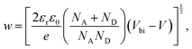
Following the bilayer strategy reported by the Bawendi group,12 solar cells are fabricated via layer-by-layer spin casting of the active layer consisting of 200 nm TBAI capped PbS, which has been shown to be n-type,19,29,30 and 60 nm EDT capped PbS, which is less n-type or even p-type depending on how much it has been oxidized.18,19 The full structure including TiO2 and MoO3/Au electrodes is shown in Fig. 1. The JV curves measured under AM1.5G 1 Sun intensity are shown in Fig. 1a and b and the corresponding parameters are displayed in Fig. 1c; at room temperature the solar cell displays a VOC of 0.61 V, a JSC of 25.8 mA cm−2, a FF of 0.60, and an overall power conversion efficiency (PCE) of 9.4%, which is higher than previous reports with a similar device structure.12 The JSC is in good agreement with the current density of 24.5 mA cm−2 calculated from the external quantum efficiency (EQE) (Fig. S1, ESI†).
 |
| | Fig. 1 (a) JV curves under 1 Sun illumination in the temperature range of 295–230 K showing increasing PCE, and (b) in the range of 230–180 K, where the PCE decreases. (c) JV curves measured in the dark. (d) Schematic of the solar cell device structure used. (e) Solar cell parameters extracted from the JV curves in (a and b) (black dots) as well as the current and voltage at the maximum power points (red dots). The solid lines are added as a guide to the eye; the dashed line is the fit for the linear part of the VOC temperature dependence. | |
As the temperature is decreased from 295 K to 180 K, the JSC remains almost constant, decreasing only about 5% over the measured range. The VOC shows a linear increase until 200 K and then plateaus at 0.80 V, or about 38% above the VOC measured at room temperature. Extrapolating the VOC from the linear regime to 0 K, a value of 1.20 eV is obtained. This is close to the bandgap of the active layer, which is 1.37 ± 0.05 eV as determined by the first excitonic peak of the EQE spectrum. This indicates that the VOC is not limited by Fermi level pinning to the trap states.31 Below 200 K, the VOC is likely limited by the energy level alignment with the TiO2 and Au electrodes.
The FF shows a more complex behaviour; it initially increases with decreasing temperature until a maximum at 250 K and then decreases at lower temperature. Overall, the JV parameters cause the PCE to initially increase with decreasing temperature to a maximum of 10.3% at 230 K, mainly due to the increasing VOC. At temperatures lower than 230 K, the FF dominates the behavior of the solar cells, leading to an overall decreasing of the PCE with decreasing temperature.
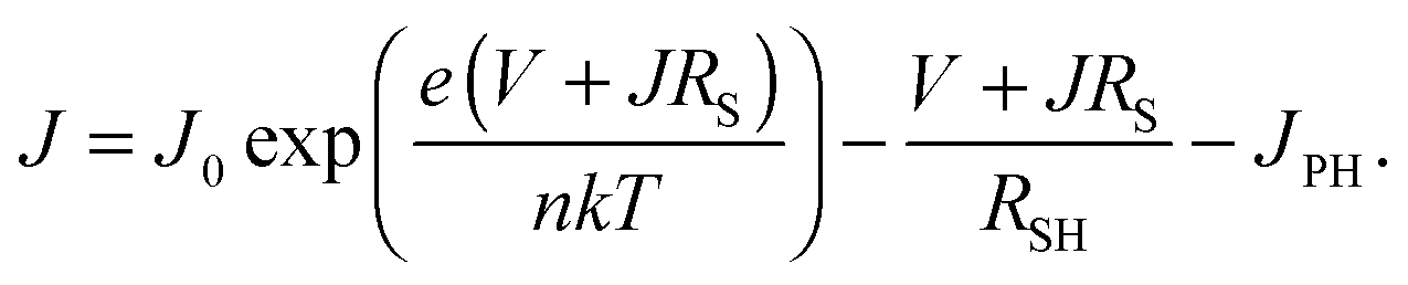
The increase in VOC cannot be explained by a changing bandgap. Photoluminescence measurements (Fig. S2, ESI†) show that as the temperature is decreased, the bandgap in fact narrows, and a smaller VOC would be expected as a result. To explain the behaviour of the solar cell parameters, and in particular the very desirable increase in VOC, we look at the Shockley diode equation for the current J,
| | 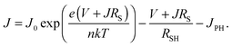 | (1) |
Here
J0 is the reverse saturation current,
e is the elementary charge,
RS and
RSH are the series and shunt resistances, respectively,
n is the ideality factor,
k is Boltzmann's constant, and
V is the applied bias. Rearranging this equation to open circuit conditions (
J = 0), and assuming that the shunt current is much smaller than the photocurrent (
V/
RSH ≪
JPH), we find that the open circuit voltage is given by
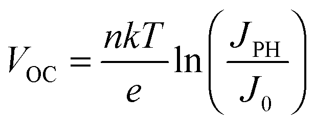
| |  | (2a) |
| |  | (2b) |
For the latter equality, we have made use of the relationship
JPH ∝
Iα, where
I is the illumination intensity,
α is an empirical parameter indicating the linearity of the photocurrent with intensity, and
c is a fitting parameter collecting all the terms independent of light intensity. From
eqn (2a), we see that the temperature affects the
VOC directly
via the linear term, and indirectly
via J0 and possibly the ideality factor
n. As shown above, the variation of
JPH with temperature is small and thus has a negligible effect on the
VOC. Since the
VOC increases with decreasing temperature, the linear term in
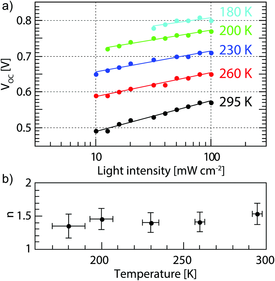
eqn (2a) is clearly not the dominating factor. The temperature dependence of the ideality factor was measured under various illuminations under open circuit conditions, as shown in
Fig. 2. In our devices
α is equal to 0.95 ± 0.3 at all temperatures measured (Fig. S3, ESI
†), which indicates that bimolecular recombination is low in these solar cells. Over a wide range of temperatures, no change is seen in the ideality factor within the measurement error. An ideality factor close to unity indicates that the dominant recombination process is bimolecular, while an ideality factor close to 2 indicates mostly trap-assisted recombination. Thus, from our measurements we can conclude that bimolecular and trap assisted recombination both play a significant role in our devices and that the relative contributions of the two do not change significantly with temperature. Therefore, the only remaining term to explain the increased
VOC as from
eqn (2a) is the reverse saturation current, which is known to be temperature dependent.
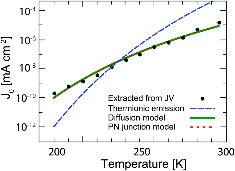
Fig. 3 shows
J0 extracted from the dark
JV measurements (
Fig. 1d) fitted with the least squares method to the explicit form of the non-ideal Shockley equation using the Lambert-W function.
32 Several models can be used to explain the temperature dependence of
J0. The most common in the case of QD solar cells are the thermionic emission model
25,33,34 and the diffusion model.
26,35 According to the thermionic emission model,
J0 is given by
| | 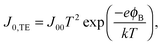 | (3) |
where
J00 is the effective Richardson's constant, equal to 120 A cm
−2 K
−2, and
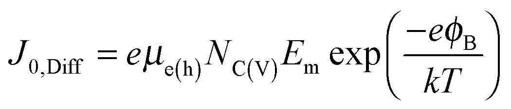
ϕB is the Schottky barrier height. The diffusion model on the other hand predicts a reverse saturation current given by
36| | 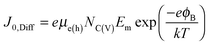 | (4) |
where
μe(h) is the majority carrier mobility,
NC(V) is the density of states in the conduction (valence) band, and
Em is the maximum electric field in the device. Finally, the reverse saturation current given by a regular PN junction is given by
36| |  | (5) |
where
NA and
ND are the acceptor and donor concentrations of the p and n type layers, respectively,
τe and
τh are the minority carrier lifetimes, and
Eg is the bandgap. Without making assumptions about any of the unknown parameters, the extracted
J0 values are fitted to each of these models in
Fig. 3. The diffusion and PN model both provide a good fit within measurement error to the experimental data, while the best fit for the thermionic emission model predicts too high a temperature dependence. The thermionic emission and diffusion models are both based on the presence of a Schottky barrier, which is not present in our devices. Instead, the PN junction model is physically more applicable to the solar cells investigated here. It is important to underline that this model gives us insight into how the reverse saturation current can be decreased in order to increase the
VOC in future solar cells at room temperature. The term in the exponent shows that a trivial method to enhance the
VOC is to increase the bandgap. However, this will simultaneously decrease the amount of photons absorbed and the generated carriers and thus the
JSC. It is also well known that for a high
VOC, recombination should be suppressed. This is reflected in the carrier lifetime terms
τe and
τh, which should be maximized. This can be achieved by reducing the trap density, to which much effort in the colloidal QD field is already being directed. Less attention has so far been directed to increasing the doping concentrations in the p and n layers. This should not only increase the
VOC through the reduction of
J0, but can help increase the built-in electric field, which facilitates charge extraction. Furthermore, it appears as a linear term in the reverse saturation current as opposed to only a square root dependence of the carrier lifetime, thus we posit that optimizing the doping concentration is a more effective strategy method to further increase the solar cell efficiency of PbS QDs. Finally, from
eqn (5) we see that while a high mobility is desirable for charge extraction and thus necessary for high
JSC, it has a weakly detrimental effect on the reverse saturation current, possibly leading to an unavoidable tradeoff between
VOC and
JSC.
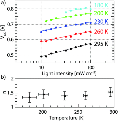 |
| | Fig. 2 (a) Light intensity dependent VOC values (dots) at different temperatures and the fits from eqn (2a) (solid lines) and (b) the ideality factors extracted from (a) showing an approximately constant ideality factor. | |
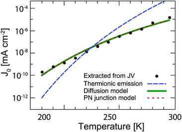 |
| | Fig. 3 Temperature dependence of the reverse saturation current extracted from dark JV curves (black dots). The data are fitted with the thermionic emission theory (dashed blue line), diffusion theory (solid green line), and the PN-junction model (dotted red line). Note that the latter two fits virtually overlap. | |
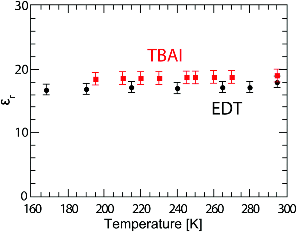
2.2 Permittivity and mobility
In order to better understand the behaviour of these solar cells at lower temperature, it is important to know whether the permittivity of the material is changing, since the permittivity not only influences recombination rates,37 but also determines the necessary exciton dissociation energy,38 plays an important role in the optical field distribution in solar cells,39 and will subsequently be used in the calculation of the charge carrier mobility. For this, we fabricated Schottky devices with the structure ITO/PEDOT:PSS/PbS/LiF/Al with either EDT or TBAI ligands, and the capacitance of the films is measured at several temperatures between 290 K and 190 K. For the geometric permittivity to be accurately obtained from the capacitance measurements, the device must be fully depleted. For this reason we make these devices thinner (∼110–150 nm) than the solar cell active layer, and measure under reverse bias to ensure the device is depleted. To verify this, the capacitance is measured at several voltages and is found not to change significantly between 0 V and −0.5 V, see Fig. S4 (ESI†). The permittivity is calculated from the average capacitance in the frequency range of 103–104 Hz, since here the capacitance is well behaved and flat, and using the parallel plate capacitor model C = (Aεrε0)/d, where A is the area defined by the overlap of the electrodes equal to 0.16 cm2 in our devices, d is the layer thickness, and εr and ε0 are the relative and vacuum permittivity, respectively. Here we consider the PEDOT:PSS layer to be part of the anode and neglect its contribution to the total capacitance of the device. The permittivity obtained in this way for various temperatures is plotted in Fig. 4. The obtained εr values for EDT decrease slightly from 18.0 ± 0.9 at room temperature to 16.8 ± 0.9 at 168 K. The permittivity of TBAI capped PbS instead remains constant within measurement error at a value of 18.7 ± 1.0.
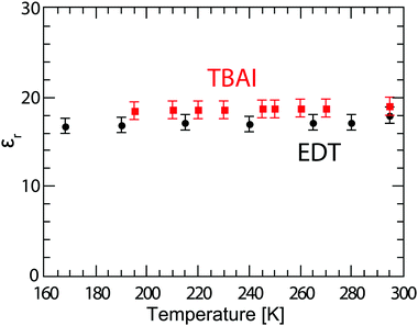 |
| | Fig. 4 Permittivity of PbS QD films capped with EDT (black dots) and TBAI (red squares), calculated using the parallel plate model from capacitance measurements averaged over the frequency 103–104 Hz. The error bars represent the measurement uncertainty over a single device, dominated by the uncertainty in film thickness. | |
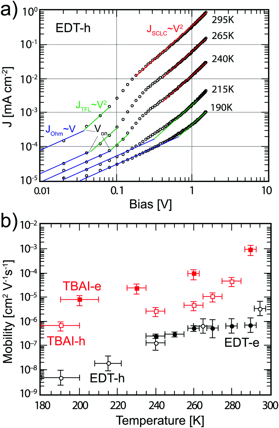
Eqn (5) shows that charge carrier mobility, doping concentration, and carrier lifetime are important parameters that determine the overall device performance. It is therefore useful to investigate each of these parameters in turn. To measure the temperature dependent mobility in the active layer, single charge carrier devices are fabricated with EDT and TBAI capped PbS. Unlike field effect transistors (FETs) or Hall effect measurements, which probe the mobility in the plane of the substrate, single charge carrier devices allow the out of plane mobility to be determined, i.e. in the same device configuration as the solar cell. Hole only devices were fabricated using device structure ITO/PEDOT:PSS/PbS/MoO3/Au, since both PEDOT:PSS and MoO3/Au are hole selective contacts aligning favorably to the PbS valence band. Silver or aluminum contacts both allow close alignment with the conduction band of PbS (∼−4.0 eV), therefore either Ag/PbS/Ag or Ag/PbS/LiF/Al device structures are used for electron only devices. JV curves of devices exhibiting space charge limited current (SCLC) in the presence of shallow traps show four characteristic regions.40,41 At low bias, thermally generated charges outnumber the injected charge carriers, and the device follows Ohm's law (J ∝ V). At a certain voltage Von, the injected charges exceed the thermally generated charges and they also fill the trap states leading to trap-filling SCLC behaviour:
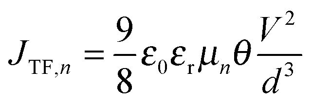
| | 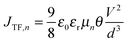 | (6) |
Here,
θ is the ratio of free charge carriers to the total carrier density,
V is the applied bias, and
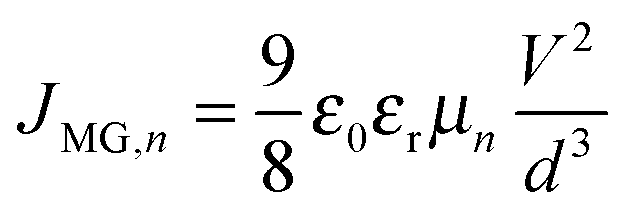
d is the device thickness. When all the traps are filled, the device shows an exponential current injection. Since the contacts allow only one charge carrier to be injected into the device, a self-limiting space charge builds up and the device follows Mott–Gurney behaviour
| |  | (7) |
The
JV characteristics for hole only devices with EDT capped PbS are shown in
Fig. 5a. For these measurements, we perform an analysis similar to the one proposed by Jeong
et al.40 Of the four regimes, the Ohmic, injection, and Mott–Gurney regimes are clearly evident; the trap-filling regime is less pronounced, but is taken to be in the region where the log–log slope of the
JV curve equals 2. From the ratio of
JTF,h and
JMG,h we find a
θ value of 0.70 at room temperature, indicating that approximately 30% of charge carriers are trapped, which increases to 0.98 at 240 K. We extract the mobility using the Mott–Gurney region for the temperatures where this is possible. At lower temperatures, only the Ohmic and trap-filling regions can be seen because
Von increases with lower temperature and pushes the Mott–Gurney regime to higher biases outside the range of the
JV curve. For those temperatures, we extract
μh from the trap-filling region with the assumption that
θ remains approximately constant. Since
θ cannot exceed unity, the error made with this assumption is small. The extracted mobilities are plotted in
Fig. 5b. At room temperature, a mobility of 3 × 10
−6 cm
2 V
−1 s
−1 is found, lower than the value of 1 × 10
4 cm
2 V
−1 s
−1 found by Rath
et al. with the structure ITO/PbS/Au.
42 With decreasing temperature, the mobility decreases almost three orders of magnitude to 5 × 10
−9 cm
2 V
−1 s
−1 at 190 K. These results are in agreement with the results found by Jeong
et al.,
40 though the temperature dependence is slightly more pronounced in our devices. We then perform similar analyses on electron only devices with EDT capped PbS QDs and TBAI capped QDs. The
JV characteristics are shown in Fig. S5 (ESI
†) while the extracted mobilities are summarized in
Fig. 5b. The data show that the EDT capped PbS films are slightly p-type, exhibiting one order of magnitude higher hole mobility than electron mobility at room temperature. In contrast the TBAI capped films display one order of magnitude higher electron mobility indicating slightly n-type behaviour, as has been previously reported in the literature.
19,43 Furthermore, at room temperature the mobility found in TBAI capped films is more than an order of magnitude higher for holes (5 × 10
−5 cm
2 V
−1 s
−1) and almost four orders of magnitude higher for electrons (1 × 10
−3 cm
2 V
−1 s
−1) than the one of EDT capped PbS. Both the hole and electron mobility of TBAI capped PbS decreases roughly two orders of magnitude between room temperature and 200 K, while the electron mobility for EDT capped PbS shows the least influence from temperature, decreasing from 7 × 10
−7 cm
2 V
−1 s
−1 to 2 × 10
−7 cm
2 V
−1 s
−1 between room temperature and 240 K.
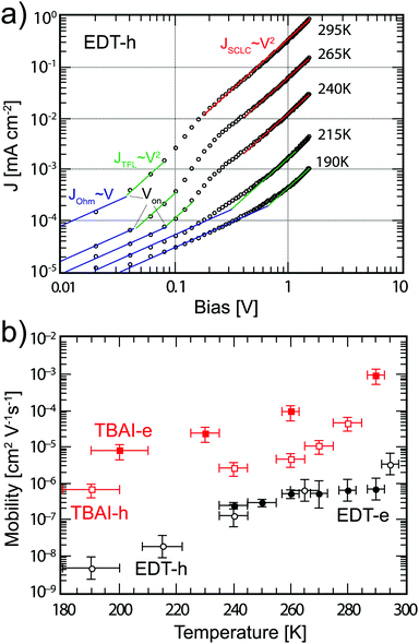 |
| | Fig. 5 (a) JV curves for hole only device with structure ITO/PEDOT:PSS/PbS_EDT/MoO3/Au at various temperatures. The solid lines indicate the Ohmic regime (blue), trap-filling regime (green) and SCLC regime (red). (b) Extracted mobilities from single carrier devices for EDT (black circles) and TBAI (red squares), for both electrons (solid markers) and holes (empty markers). The error bars represent the measurement uncertainty over a single device resulting mainly from the uncertainty in film thickness. | |
Field effect mobilities are also measured for comparison. For this, SiO2 gated FETs were fabricated by depositing EDT and TBAI capped films with the same recipe as the solar cells and measured in a vacuum. Charge carrier mobility values are extracted from the linear regime according to the gradual channel approximation and using a parallel plate capacitor model for the gate electrode charge accumulation. In contrast to the SCLC devices, the FETs show initially increasing mobility with decreasing temperature, which may indicate band like transport (Fig. S6, ESI†). The FET mobility values follow the same trend as previously reported for PbS QDs using the Hall effect and FET measurements,44 and FET mobilities of CdSe QDs.45 Hall effect measurements only probe the mobility of the non-trapped charge carriers,44 and in FETs the Fermi level is raised by the gate bias such that most traps are filled.6 Therefore, the Hall effect and FET analyses both give mobility values closer to the trap free mobility of PbS QDs, but which are far from the effective mobility in solar cell configuration. The mobility results from our SCLC devices likely indicate a high trap density in PbS QD films that prevents band-like transport under low biasing conditions; given this high trap density, a decrease in the temperature means less thermal energy is available to re-excite charge carriers from shallow traps back to the transport levels, lowering the overall mobility. Furthermore, we observe that in contrast to the SCLC devices, the FETs with EDT capped PbS display notably higher electron mobility. This can be explained by the vacuum environment used for the temperature dependent FET measurements, since vacuum can reverse the ambient p-doping effect of thiol capped PbS, as observed previously by Balazs et al.18
2.3 Charge carrier lifetimes and diffusion lengths
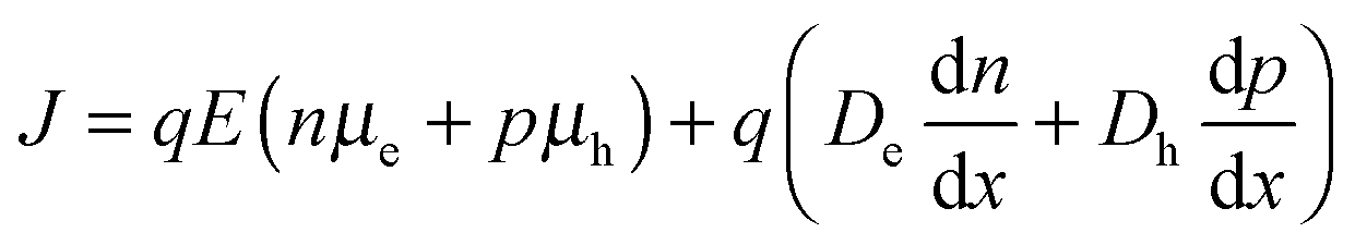
Charge carrier mobility plays an important role in determining whether or not generated charges can be extracted from solar cells before recombining. It is therefore interesting to note that despite the trend of decreasing mobility, as measured using the single carrier devices, the JSC value does not decrease very much. The current density in a diode is given by the sum of the drift and diffusion currents,| | 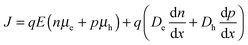 | (8) |
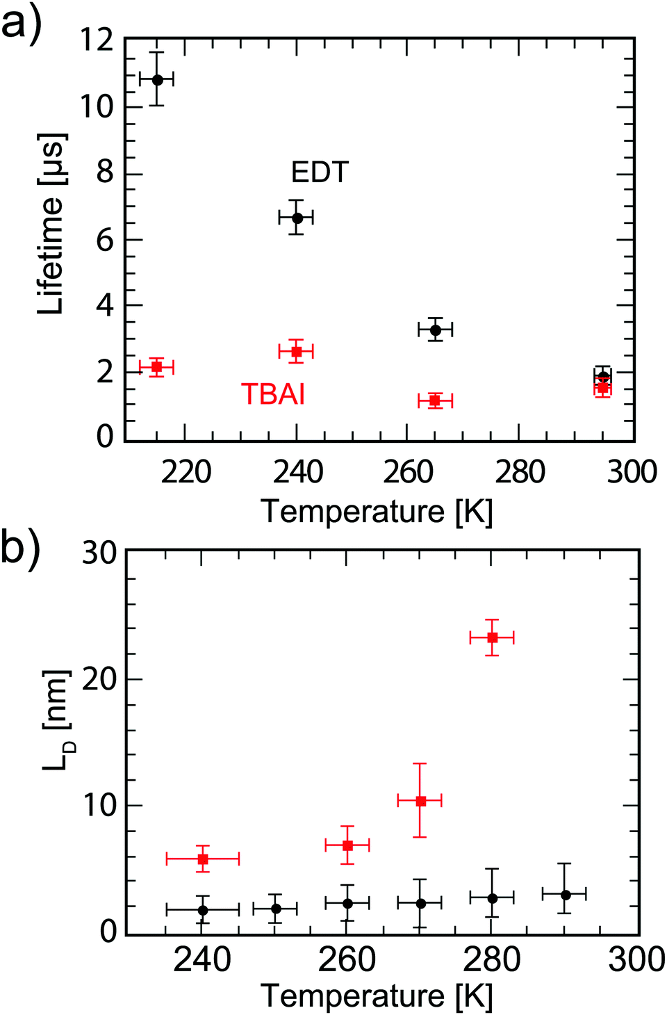
where n and p are the electron and hole concentration, respectively, E is the electric field in the device caused by the built-in electric field and the applied bias, and De and Dh are the electron and hole diffusion coefficients given by De/h = (kT/q)μe/h. Charges from outside the depletion region must diffuse to the region where there is an electric field to drive their transport. Charges generated in regions further away from the depletion region than their diffusion length recombine before they can be extracted and therefore do not contribute to the photocurrent. To determine the diffusion length in our solar cells, it is necessary to measure not only the mobility, but also the lifetime of photogenerated charge carriers. For this, Schottky devices with structure ITO/PEDOT:PSS/PbS/LiF/Al are fabricated with both EDT and TBAI ligands and the capacitance is measured under 1 Sun illumination under open circuit conditions. Since no current leaves the device at VOC, all generated charges must recombine, and the characteristic lifetime of the process can be found from the product of the recombination resistance and the chemical capacitance τn = RrCμ.46,47 The Nyquist plots obtained are shown in Fig. S7 (ESI†) and are fitted with the simple three component model shown in the inset. The lifetimes obtained therefrom are displayed in Fig. 6a. It is important to note that these are the lifetimes of the minority carriers in their respective layers, i.e., the electron lifetime for EDT capped PbS and hole lifetime for TBAI capped PbS. EDT capped PbS displays carrier lifetimes of 2 μs at room temperature, in close agreement with the values measured by Bawendi et al. using transient photovoltage measurements,24 which increases slightly to 13 μs at 215 K. The carrier lifetimes in TBAI capped films are also 2 μs at room temperature but do not show significant temperature dependence in the measured range. With the lifetime and mobility known, the diffusion length can easily be calculated from  , where
  is Einstein's diffusion coefficient, and is shown in Fig. 6b. The electron diffusion length in EDT capped PbS is found to be extremely short, around 3.0 ± 1.5 nm, which is significantly shorter than reported values for PbS coupled with MPA (30 ± 10 nm) or with MPA + CdCl2 (80 ± 10 nm).48 Owing to the higher mobility, TBAI capped PbS displays a higher diffusion length at room temperature of 23 ± 3 nm, which decreases to 5.7 ± 1 nm at 240 K. Considering the solar cell thickness of 260 nm and the fact that the JSC does not drop significantly between room temperature and 240 K (Fig. 1d), the declining diffusion length for TBAI capped PbS and very small diffusion length for EDT capped PbS indicate that the solar cells are practically fully depleted under short circuit conditions.
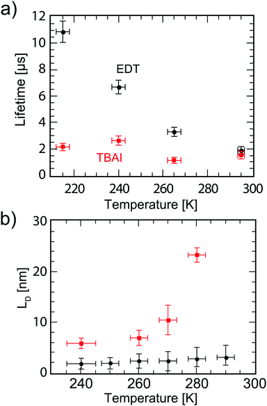 |
| | Fig. 6 (a) Carrier lifetime for electrons in EDT capped PbS (black dots), and holes in TBAI capped PbS (red squares) obtained with impedance spectroscopy measurements under 1 Sun illumination under open circuit conditions. (b) Diffusion lengths of electrons in EDT capped PbS (black dots) and holes in TBAI capped PbS (red squares) calculated from  using the mobilities as reported in Fig. 5b and lifetimes from (a). The error bars represent the measurement uncertainty over a single device following from the uncertainty in mobility and carrier lifetime. using the mobilities as reported in Fig. 5b and lifetimes from (a). The error bars represent the measurement uncertainty over a single device following from the uncertainty in mobility and carrier lifetime. | |
2.4 Doping concentration
The doping concentrations in the n and p layers together determine both the degree of band bending and the distribution of the depletion width w via Nawp = Ndwn. In most silicon solar cells, the main absorbing layer has a moderate (usually p-type) doping concentration of 1016–1017 cm−3, followed by a highly doped (usually n-type) layer. This leads to a large depletion width in the absorbing layer, allowing most photogenerated charges to be swept out of the device without relying on diffusion. To determine the doping concentrations in our solar cells we again investigate Schottky diodes with the structure ITO/PEDOT:PSS/PbS/LiF/Al. From the Mott–Schottky equation,| | 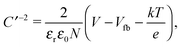 | (9) |
the doping concentration N can be obtained from the slope of C′−2versus the applied bias V. For this, the capacitance is measured with a 4.6 kHz AC bias with an amplitude of 10 mV superimposed on a DC bias ranging from 0 to 1 V at various temperatures. The Mott–Schottky curves are shown in Fig. S8 (ESI†) and the extracted doping concentrations are plotted in Fig. 7a. EDT capped PbS shows a doping concentration of (1.0 ± 0.4) × 1017 cm−3, which remains essentially constant over the measured temperature range. TBAI capped PbS exhibits a doping concentration at room temperature of (4.6 ± 2.3) × 1016 cm−3, which decreases to (1.5 ± 0.5) × 1016 cm−3 at 215 K.
 |
| | Fig. 7 (a) Doping concentration of EDT (black dots) and TBAI (red squares) capped PbS measured by Mott–Schottky analysis. The error bars are determined by the uncertainty in permittivity, slopes of the Mott–Schottky curves, and temperature. (b) Depletion width calculated at zero bias (black) and at the maximum power point (red). The dashed line shows the device thickness. The error bars originate from the uncertainty in the permittivity and doping concentrations. | |
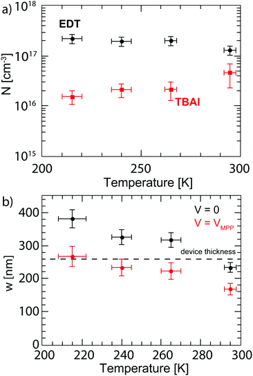
With the doping concentration known, the depletion width w can be calculated by49
| |  | (10) |
where
NA and
ND are the acceptor and donor concentrations, and
Vbi is the built-in potential. The depletion width is calculated for varying temperature at zero bias and at the maximum operating point, shown in
Fig. 7b. At room temperature under short circuit conditions the depletion width is found to be 234 ± 15 nm. Therefore the depletion width plus diffusion length covers almost the whole device thickness of 260 nm. As the temperature is decreased, the depletion region increases leading to full depletion of the device below ∼280 °C. This can explain why the short circuit current does not change with decreasing temperature despite the lower mobility. Under maximum power point conditions, the depletion width shows a similar trend but is ∼30% lower, such that
w is only 168 ± 17 nm at room temperature, which limits the collection efficiency of charges outside the depletion region and explains why
JMPP is significantly lower than the
JSC, leading to a relatively low FF in these devices.
For depletion widths smaller than the device thickness, it is important to optimize the distribution of the depletion width over the pn-junction. Given that the mobility of TBAI capped PbS is significantly higher than in the EDT capped layer, it is desirable to use the TBAI layer as the main absorber layer, and to limit the thickness of the EDT layer. With these doping concentrations, 64% of the depletion region is located on the TBAI side at room temperature, while at lower temperatures the depletion width shifts increasingly to the TBAI layer, such that 93% of the depletion area is located on the TBAI side at 125 K. This, together with the increasing depletion width could explain the initial increase in the fill factor between room temperature and 260 K, while at lower temperatures the decreasing mobility dominates the fill factor behaviour. Thus, to improve the efficiency at room temperature, an order of magnitude higher doping of the p-type layer is required such that practically all of the depletion width falls in the TBAI layer.
3 Conclusion
We have fabricated highly efficient PbS QD solar cells and explored their temperature dependent properties. The VOC is found to be governed solely by the reverse saturation current, which can be explained using the PN-junction model. Based on this model, we propose that increasing the doping levels in the PN-junction structure is a promising method for increasing the VOC in future QD based solar cells. In addition, the doping concentration of the p-type layer should be at least 1 order of magnitude higher than the n-type layer for a favourable depletion width distribution across the junction. Moreover, we have determined all the most important physical parameters that determine the working mechanism of our solar cells. Electron and hole mobilities were measured for both EDT and TBAI capped QD films, and were found to decrease with decreasing temperature. TBAI capped QDs showed electron and hole mobility values of 1 × 10⁻³ cm2 V−1 s−1 and 5 × 10⁻⁵ cm2 V−1 s−1, respectively, which decrease by roughly two orders of magnitude as temperature is decreased to 200 K. EDT capped films show significantly lower electron and hole mobility values of 7 × 10⁻⁷ cm2 V−1 s−1 and 3 × 10⁻⁶ cm2 V−1 s−1 respectively. Very short diffusion lengths were observed in EDT capped PbS independent of temperature between 290 K and 240 K, while TBAI capped films showed diffusion lengths decreasing from 26 ± 3 nm to 6 ± 1 nm. In spite of these short diffusion lengths the current output of our devices at JSC is almost temperature independent. This is explained by the depletion region, which is found to extend almost throughout the active layer of the solar cells at room temperature and to extend completely throughout the device at lower temperatures. Thus, these solar cells are not limited by diffusion, instead they rely on drift-dominated transport for charge carrier extraction.
4 Experimental methods
Device fabrication
TiO2 is formed by spincasting a 20![[thin space (1/6-em)]](https://www.rsc.org/images/entities/char_2009.gif) :2:1 solution of ethanol:titanium(IV) butoxide:HCl onto pre-patterned fluorine doped tin-oxide substrates (13 Ω sq−1) and annealed at 450 °C for 30 min. Oleic acid capped PbS QDs are synthesized by a previously described hot injection method.23,46 QD films are made in a N2 glovebox by layer-by-layer spincasting a 10 mg ml−1 solution of PbS in hexane and exposing the film to either EDT (0.01% vv in actetonitrile) or TBAI (15 mg ml−1 in methanol) for 30 s before spin drying. The film is then washed twice in the solvent of the ligand and spin-dried. This process is repeated until the desired thickness is achieved. Under <10−6 mBar vacuum, the solar cells are finished by thermal evaporation of 5 nm MoO3 and 80 nm Au at a rate of 0.2 Å s−1 and 2 Å s−1, respectively. In total, 30 solar cells with this structure were fabricated on 12 different substrates and the analysis reported here was performed on the champion device. For Schottky devices the active layer is deposited on top of 90 nm poly(3,4-ethylenedioxythiophene)–poly(styrenesulfonate) (PEDOT:PSS; VP AI4083, H. C. Stark) spincasted from water and annealed at 120 °C for 10 min. The Schottky devices are finished by thermal evaporation of 1 nm LiF (0.1 Å s−1) and 100 nm Al (0.5–10 Å s−1). The device area is 0.16 cm2 as defined by the overlap of electrodes.
:2:1 solution of ethanol:titanium(IV) butoxide:HCl onto pre-patterned fluorine doped tin-oxide substrates (13 Ω sq−1) and annealed at 450 °C for 30 min. Oleic acid capped PbS QDs are synthesized by a previously described hot injection method.23,46 QD films are made in a N2 glovebox by layer-by-layer spincasting a 10 mg ml−1 solution of PbS in hexane and exposing the film to either EDT (0.01% vv in actetonitrile) or TBAI (15 mg ml−1 in methanol) for 30 s before spin drying. The film is then washed twice in the solvent of the ligand and spin-dried. This process is repeated until the desired thickness is achieved. Under <10−6 mBar vacuum, the solar cells are finished by thermal evaporation of 5 nm MoO3 and 80 nm Au at a rate of 0.2 Å s−1 and 2 Å s−1, respectively. In total, 30 solar cells with this structure were fabricated on 12 different substrates and the analysis reported here was performed on the champion device. For Schottky devices the active layer is deposited on top of 90 nm poly(3,4-ethylenedioxythiophene)–poly(styrenesulfonate) (PEDOT:PSS; VP AI4083, H. C. Stark) spincasted from water and annealed at 120 °C for 10 min. The Schottky devices are finished by thermal evaporation of 1 nm LiF (0.1 Å s−1) and 100 nm Al (0.5–10 Å s−1). The device area is 0.16 cm2 as defined by the overlap of electrodes.
Current–voltage characterization
JV sweeps were carried out in an inert environment using a Keithley 2400 source-meter. Simulated AM1.5G illumination was provided by a Steuernagel Solarconstant 1200 metal halide lamp set to 100 mW cm−2 intensity, measured using a silicon reference cell (SRC-1000-RTD-QZ, VLSI Standards Inc.) and corrected for the spectral mismatch.50 The illuminated area was limited to 0.10 cm2 by a well-defined shadow mask for efficiency calculations. The temperature was controlled by an adjustable N2 gas flow through a liquid N2 bath.
Impedance spectroscopy
Using a SP-200 Bio-Logic potentiostat a forward bias is superimposed with a 30 mV AC perturbation over the frequency range of 1 MHz to 100 Hz. For permittivity measurements, the capacitance is measured in the dark at −0.5 V DC bias. For carrier lifetime measurements, the device is held at open circuit bias under 1 Sun illumination.
EQE measurements
The EQE is measured under short circuit conditions under monochromatic light. As a white light source a 250 W quartz tungsten halogen lamp (6334NS, Newport) with lamp housing (67009, Newport) is used. Monochromatic light is obtained using narrow band pass filters (Thorlabs) with a full width half maximum (FWHM) of 10 ± 2 nm from 400 nm to 1300 nm and a FWHM of 12 ± 2.4 nm from 1300 nm to 1400 nm. The light intensity is determined by calibrated PD300 and PD300IR photodiodes (Ophir Optics).
PL measurements
PbS QD films were deposited on quartz substrates using the layer-by-layer technique mentioned above. The samples were excited at 400 nm by the second harmonic of a modelocked Ti:sapphire (Mira 900) laser delivering pulses of 150 fs. An optical pulse selector was used to vary the repetition rate of the exciting pulse. All measurements were performed in an optical cryostat, loaded inside a glovebox to maintain an oxygen-free environment at all times.
Acknowledgements
M. J. Speirs and M. A. Loi acknowledge the financial support of the Alumnikring Den Haag/Rotterdam through the Ubbo Emmius Fund of the University of Groningen. M. A. L. acknowledges also the support of the ERC Starting Grant “Hybrids Solution Processable Optoelectronic Devices” (Hy-SPOD) (ERC-306983); M. V. Kovalenko acknowledges partial financial support from ERC Starting Grant NANOSOLID (GA No. 306733).
References
- S. A. Mcdonald, G. Konstantatos, S. Zhang, P. W. Cyr, E. J. Klem, L. Levina and E. H. Sargent, Nat. Mater., 2005, 4, 138 CrossRef CAS PubMed.
- G. Konstantatos and E. H. Sargent, Appl. Phys. Lett., 2007, 91, 173505 CrossRef.
- K. Szendrei, F. Cordella, M. V. Kovalenko, M. Böberl, G. Hesser, M. Yarema, D. Jarzab, O. V. Mikhnenko, A. Gocalinska, M. Saba, F. Quochi, A. Mura, G. Bongiovanni, P. W. M. Blom, W. Heiss and M. A. Loi, Adv. Mater., 2009, 21, 683–687 CrossRef CAS.
- Z. Sun, Z. Liu, J. Li, G.-A. Tai, S.-P. Lau and F. Yan, Adv. Mater., 2012, 24, 5878 CrossRef CAS PubMed.
- P. Moroz, G. Liyanage, N. N. Kholmicheva, S. Yakunin, U. Rijal, P. Uprety, E. Bastola, B. Mellott, K. Subedi, L. Sun, M. V. Kovalenko and M. Zamkov, Chem. Mater., 2014, 26, 4256 CrossRef CAS.
- S. Z. Bisri, C. Piliego, M. Yarema, W. Heiss and M. A. Loi, Adv. Mater., 2013, 25, 4309 CrossRef CAS PubMed.
- M. I. Nugraha, R. Häusermann, S. Z. Bisri, H. Matsui, M. Sytnyk, W. Heiss, J. Takeya and M. A. Loi, Adv. Mater., 2015, 27, 2107 CrossRef CAS PubMed.
- A. G. Shulga, L. Piveteau, S. Z. Bisri, M. V. Kovalenko and M. A. Loi, Adv. Electron. Mater., 2016, 2, 1500467 CrossRef.
- L.-H. Lai, M. J. Speirs, F.-K. Chang, L. Piveteau, M. V. Kovalenko, J.-S. Chen, J.-J. Wu and M. A. Loi, Appl. Phys. Lett., 2015, 107, 183901 CrossRef.
- C. Piliego, L. Protesescu, S. Z. Bisri, M. V. Kovalenko and M. A. Loi, Energy Environ. Sci., 2013, 6, 3054 CAS.
- G.-H. Kim, F. P. García de Arquer, Y. J. Yoon, X. Lan, M. Liu, O. Voznyy, Z. Yang, F. Fan, A. H. Ip, P. Kanjanaboos, S. Hoogland, J. Y. Kim and E. Sargent, Nano Lett., 2015, 15, 7691 CrossRef CAS PubMed.
- C.-H. M. Chuang, P. R. Brown, V. Bulović and M. G. Bawendi, Nat. Mater., 2014, 13, 796 CrossRef CAS PubMed.
- M. P. Hendricks, M. P. Campos, G. T. Cleveland, I. Jen-La Plante and J. S. Owen, Science, 2015, 348, 1226 CrossRef CAS PubMed.
- I. Lignos, L. Protesescu, S. Stavrakis, L. Piveteau, M. J. Speirs, M. A. Loi, M. V. Kovalenko and A. J. deMello, Chem. Mater., 2014, 26, 2975 CrossRef CAS.
- A. H. Ip, S. M. Thon, S. Hoogland, O. Voznyy, D. Zhitomirsky, R. Debnath, L. Levina, L. R. Rollny, G. H. Carey, A. Fischer, K. W. Kemp, I. J. Kramer, Z. Ning, A. J. Labelle, K. W. Chou, A. Amassian and E. H. Sargent, Nat. Nanotechnol., 2012, 7, 577 CrossRef CAS PubMed.
- K. S. Jeong, J. Tang, H. Liu, J. Kim, A. W. Schaefer, K. Kemp, L. Levina, X. Wang, S. Hoogland, R. Debnath, L. Brzozowski, E. H. Sargent and J. B. Asbury, ACS Nano, 2011, 6, 89–99 CrossRef PubMed.
- J. Tang, K. W. Kemp, S. Hoogland, K. S. Jeong, H. Liu, L. Levina, M. Furukawa, X. Wang, R. Debnath, D. Cha, K. W. Chou, A. Fischer, A. Amassian, J. B. Asbury and E. H. Sargent, Nat. Mater., 2011, 10, 765 CrossRef CAS PubMed.
- D. M. Balazs, M. I. Nugraha, S. Z. Bisri, M. Sytnyk, W. Heiss and M. A. Loi, Appl. Phys. Lett., 2014, 104, 112104 CrossRef.
- P. R. Brown, D. Kim, R. R. Lunt, N. Zhao, M. G. Bawendi, J. C. Grossman and V. Bulović, ACS Nano, 2014, 8, 5863 CrossRef CAS PubMed.
- P. Maraghechi, A. J. Labelle, A. R. Kirmani, X. Lan, M. M. Adachi, S. M. Thon, S. Hoogland, A. Lee, Z. Ning, A. Fischer, A. Amassian and E. H. Sargent, ACS Nano, 2013, 7, 6111 CrossRef CAS PubMed.
- J. Tang, H. Liu, D. Zhitomirsky, S. Hoogland, X. Wang, M. Furukawa, L. Levina and E. H. Sargent, Nano Lett., 2012, 12, 4889–4894 CrossRef CAS PubMed.
- D.-K. Ko, P. R. Brown, M. G. Bawendi and V. Bulović, Adv. Mater., 2014, 26, 4845–4850 CrossRef CAS PubMed.
- M. J. Speirs, D. M. Balazs, H.-H. Fang, L.-H. Lai, L. Protesescu, M. V. Kovalenko and M. A. Loi, J. Mater. Chem. A, 2015, 3, 1450 CAS.
- C.-H. M. Chuang, A. Maurano, R. E. Brandt, G. W. Hwang, J. Jean, T. Buonassisi, V. Bulović and M. G. Bawendi, Nano Lett., 2015, 15, 3286–3294 CrossRef CAS PubMed.
- D. Bozyigit, W. M. Lin, N. Yazdani, O. Yarema and V. Wood, Nat. Commun., 2015, 6 DOI:10.1038/ncomms7180.
- K. Szendrei, M. Speirs, W. Gomulya, D. Jarzab, M. Manca, O. V. Mikhnenko, M. Yarema, B. J. Kooi, W. Heiss and M. A. Loi, Adv. Funct. Mater., 2012, 22, 1598 CrossRef CAS.
- D.-K. Ko, A. Maurano, S. K. Suh, D. Kim, G. W. Hwang, J. C. Grossman, V. Bulović and M. G. Bawendi, ACS Nano, 2016, 10, 3382 CrossRef CAS PubMed.
- D. M. Balazs, D. N. Dirin, H.-H. Fang, L. Protesescu, G. H. ten Brink, B. J. Kooi, M. V. Kovalenko and M. A. Loi, ACS Nano, 2015, 11951–11959 CrossRef CAS PubMed.
- Z. Ning, H. Dong, Q. Zhang, O. Voznyy and E. H. Sargent, ACS Nano, 2014, 8, 10321 CrossRef CAS PubMed.
- Z. Ning, O. Voznyy, J. Pan, S. Hoogland, V. Adinolfi, J. Xu, M. Li, A.
R. Kirmani, J.-P. Sun, J. Minor, K. W. Kemp, H. Dong, L. Rollny, A. Labelle, G. Carey, B. Sutherland, I. Hill, A. Amassian, H. Liu, J. Tang, O. M. Bakr and E. H. Sargent, Nat. Mater., 2014, 13, 822 CrossRef CAS PubMed.
- A. Rath, F. P. García de Arquer, A. Stavrinadis, T. Lasanta, M. Bernechea, S. L. Diedenhofen and G. Konstantatos, Adv. Mater., 2014, 26, 4741 CrossRef CAS PubMed.
- A. Jain and A. Kapoor, Sol. Energy Mater. Sol. Cells, 2004, 81, 269 CrossRef CAS.
- A. Heidaripour, M. Jafarian, F. Gobal, M. Mahjani and S. Miandari, J. Appl. Phys., 2014, 116, 034906 CrossRef.
- J. Gao, J. M. Luther, O. E. Semonin, R. J. Ellingson, A. J. Nozik and M. C. Beard, Nano Lett., 2011, 11, 1002 CrossRef CAS PubMed.
- J. P. Clifford, K. W. Johnston, L. Levina and E. H. Sargent, Appl. Phys. Lett., 2007, 91, 253117 CrossRef.
-
S. M. Sze and K. K. Ng, Physics of Semiconductor Devices, Wiley, Hoboken, NJ, USA, 2007 Search PubMed.
- B. L. Wehrenberg, C. Wang and P. Guyot-Sionnest, J. Phys. Chem. B, 2002, 106, 10634 CrossRef CAS.
- G. D. Scholes and G. Rumbles, Nat. Mater., 2006, 5, 683–696 CrossRef CAS PubMed.
- L. Pettersson, L. Roman and O. Inganäs, J. Appl. Phys., 1999, 86, 487 CrossRef CAS.
- J. K. Kim, J. H. Song, H. Choi, S. J. Baik and S. Jeong, J. Appl. Phys., 2014, 115, 054302 CrossRef.
- K. M. Kim, B. J. Choi, Y. C. Shin, S. Choi and C. S. Hwang, Appl. Phys. Lett., 2007, 91, 12907–13100 CrossRef.
- A. K. Rath, T. Lasanta, M. Bernechea, S. L. Diedenhofen and G. Konstantatos, Appl. Phys. Lett., 2014, 104, 063504 CrossRef.
- D. Zhitomirsky, M. Furukawa, J. Tang, P. Stadler, S. Hoogland, O. Voznyy, H. Liu and E. H. Sargent, Adv. Mater., 2012, 24, 6181 CrossRef CAS PubMed.
- J. Jang, W. Liu, J. S. Son and D. V. Talapin, Nano Lett., 2014, 14, 653–662 CrossRef CAS PubMed.
- J.-H. Choi, A. T. Fafarman, S. J. Oh, D.-K. Ko, D. K. Kim, B. T. Diroll, S. Muramoto, J. G. Gillen, C. B. Murray and C. R. Kagan, Nano Lett., 2012, 12, 2631 CrossRef CAS PubMed.
- L.-H. Lai, L. Protesescu, M. V. Kovalenko and M. A. Loi, Phys. Chem. Chem. Phys., 2014, 16, 736 RSC.
- X.-Y. Yu, J.-Y. Liao, K.-Q. Qiu, D.-B. Kuang and C.-Y. Su, ACS Nano, 2011, 5, 9494–9500 CrossRef CAS PubMed.
- D. Zhitomirsky, O. Voznyy, S. Hoogland and E. H. Sargent, ACS Nano, 2013, 7, 5282–5290 CrossRef CAS PubMed.
-
P. Würfel, Physics of Solar Cells, Wiley, Hoboken, NJ, USA, 2009 Search PubMed.
- J. M. Kroon, M. M. Wienk, W. J. H. Verhees and J. C. Hummelen, Thin Solid Films, 2002, 403, 223 CrossRef.
Footnote |
| † Electronic supplementary information (ESI) available. See DOI: 10.1039/c6ee01577h |
|
| This journal is © The Royal Society of Chemistry 2016 |
Click here to see how this site uses Cookies. View our privacy policy here. 
 Open Access Article
 This Open Access Article is licensed under a
  a,
Dmitry N.
Dirin
a,
Dmitry N.
Dirin

 , where
  is Einstein's diffusion coefficient, and is shown in Fig. 6b. The electron diffusion length in EDT capped PbS is found to be extremely short, around 3.0 ± 1.5 nm, which is significantly shorter than reported values for PbS coupled with MPA (30 ± 10 nm) or with MPA + CdCl2 (80 ± 10 nm).48 Owing to the higher mobility, TBAI capped PbS displays a higher diffusion length at room temperature of 23 ± 3 nm, which decreases to 5.7 ± 1 nm at 240 K. Considering the solar cell thickness of 260 nm and the fact that the JSC does not drop significantly between room temperature and 240 K (Fig. 1d), the declining diffusion length for TBAI capped PbS and very small diffusion length for EDT capped PbS indicate that the solar cells are practically fully depleted under short circuit conditions.
 using the mobilities as reported in Fig. 5b and lifetimes from (a). The error bars represent the measurement uncertainty over a single device following from the uncertainty in mobility and carrier lifetime.

